US5719973A - Optical waveguides and components with integrated grin lens - Google Patents
Optical waveguides and components with integrated grin lens Download PDFInfo
- Publication number
- US5719973A US5719973A US08/688,324 US68832496A US5719973A US 5719973 A US5719973 A US 5719973A US 68832496 A US68832496 A US 68832496A US 5719973 A US5719973 A US 5719973A
- Authority
- US
- United States
- Prior art keywords
- diameter
- optical device
- light
- transceiving end
- longitudinal axis
- Prior art date
- Legal status (The legal status is an assumption and is not a legal conclusion. Google has not performed a legal analysis and makes no representation as to the accuracy of the status listed.)
- Expired - Lifetime
Links
Images


Classifications
-
- G—PHYSICS
- G02—OPTICS
- G02B—OPTICAL ELEMENTS, SYSTEMS OR APPARATUS
- G02B6/00—Light guides; Structural details of arrangements comprising light guides and other optical elements, e.g. couplings
- G02B6/02—Optical fibres with cladding with or without a coating
- G02B6/028—Optical fibres with cladding with or without a coating with core or cladding having graded refractive index
- G02B6/0281—Graded index region forming part of the central core segment, e.g. alpha profile, triangular, trapezoidal core
-
- G—PHYSICS
- G02—OPTICS
- G02B—OPTICAL ELEMENTS, SYSTEMS OR APPARATUS
- G02B6/00—Light guides; Structural details of arrangements comprising light guides and other optical elements, e.g. couplings
- G02B6/24—Coupling light guides
- G02B6/26—Optical coupling means
- G02B6/262—Optical details of coupling light into, or out of, or between fibre ends, e.g. special fibre end shapes or associated optical elements
Definitions
- This invention relates to the coupling of optical components and devices such as optical waveguides or fibers, and in particular to the fabrication of a gradient index (GRIN) lens integral to the optical component in order to achieve high coupling efficiency of the optical components.
- GRIN gradient index
- optical components such as laser diodes, optical switches, modulators, wavelength selecting devices and the like are optically coupled together by optical fibers.
- the coupling or interconnection of such devices to a waveguide is complicated by a mismatch-between the numerical apertures of the optical device and the waveguide.
- the extremely small diameter of the optical fibers used for optical communications which is on the order of 125 ⁇ m in outer diameter with a typical core diameter of 8 ⁇ m, makes mechanical alignment of the fiber core with other optical components difficult. Since a desirable quality of an optical data transmission system is to transmit light energy with minimal loss and distortion, attempts have been made in the prior art to provide a means for aligning optical components without suffering the deleterious effects described herein.
- U.S. Pat. No. 5,163,107 discloses the use of a fiber optic coupler/connector with a GRIN lens positioned in a bore through the coupler axially aligned with the optic fiber.
- the GRIN lens conditions the light, for example collimates or expands the light signals entering and exiting the optic fiber.
- the light signals are coupled between two fiber optic cables, each fitted with the coupler described in the '107 patent, such that the coupler end plate faces are positioned adjacent to each other with common axial alignment.
- This type of combination has the disadvantage of requiring separate piece parts which need to be handled, critically aligned, and reliably attached.
- the separate GRIN lenses comprise reflective surfaces, additional performance degrading reflections are introduced into the optical system.
- U.S. Pat. No. 5,200,024 discloses a wet chemical etching technique for forming a lensed optical fiber. Although this is a desirable technique since it provides for batch processing, thus keeping manufacturing costs relatively lower, the numerical aperture is limited by the fiber dopant profile and the physical shape of the lens. In addition, etched lenses are subject to etching related defects, and the etched lens may be damaged more easily from handling. Finally, the uniform deposition of anti-reflection (AR) coatings is made more difficult by the surface topology of tapered, machined, etched or otherwise shaped lenses.
- AR anti-reflection
- the present invention is an optical component such as an optical fiber waveguide having at least one light transceiving end suitable for transmitting or receiving light, the optical component comprising: core suitable for allowing transmission therethrough of light, a cladding layer surrounding the core and having an index of refraction less than that of the core, and an embedded lens integrally located at the light transceiving end.
- the embedded lens is preferably a gradient refractive index (GRIN) lens having a refractive index that varies along a radial axis of the light transceiving end of the device and/or along a longitudinal axis of the light transceiving end of the device.
- the embedded GRIN lens is comprised of at least one dopant region having a refractive index that varies along a radial axis and/or along a longitudinal axis of the light transceiving end of the device.
- the embedded GRIN lens is comprised of a plurality of dopant regions wherein each dopant region has a predetermined diameter and extends a predetermined distance along the longitudinal axis.
- the dopant regions are configured such that the dopant region with the shortest longitudinal distance has the largest diameter and the dopant region with the longest longitudinal distance has the smallest diameter.
- the embedded GRIN lens is comprised of multiple dopant regions which comprises first dopant region extending a first distance along the longitudinal axis and having a first diameter; a second dopant region extending a second distance along the longitudinal axis and having a second diameter, the second distance being less than the first distance and the second diameter being greater than the first diameter; and subsequent dopant regions extending a predetermined distance along the longitudinal axis and having a predetermined diameter, such that each subsequent distance being less than the previous distance and each subsequent diameter being greater than the previous diameter.
- the first dopant region is formed by applying to the light transceiving end of the optical device a mask having an opening with a diameter equivalent to the first diameter, such that an area having the first diameter is exposed, and then bombarding the exposed area with ions of a first energy level.
- the second dopant region is formed by applying to the light transceiving end of the optical device a mask having an opening with a diameter equivalent to the second diameter, such that an area having the second diameter is exposed, and then bombarding the exposed area with ions of a second energy level, the second energy level being less than the first energy level.
- the subsequent dopant regions are formed by applying to the light transceiving end of the optical device a mask having an opening with a diameter equivalent to a predetermined diameter, such that an area having the diameter is exposed, and then bombarding the exposed area with ions of a subsequent energy level, the subsequent energy level being less than the prior energy level.
- the type of the ion, the ion dose level, or duration of implantation may be controlled in order to vary the ion concentration. For example, a relatively longer bombardment time will result in a relatively higher ion concentration, which will result in a relatively higher index of refraction.
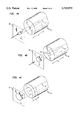
- FIG. 1 is a perspective view of an optical fiber with an embedded GRIN lens in accordance with one embodiment of the present invention
- FIG. 2 is a side cross-section view of the fiber of FIG. 1;
- FIG. 3(a) is an exemplary plot illustrating ion distribution profiles based on ion implantation energy
- FIG. 3(b) is an exemplary plot illustrating the change in refractive index as a function of ion dosage
- FIGS. 4(a) through 4(c) are illustrations of the masking steps used to fabricate the embedded GRIN lens in accordance with one embodiment of the present invention.
- FIG. 5 is a perspective illustration of an array of fibers being processed in accordance with an embodiment of the present invention.
- a fiber optic waveguide 10 is illustrated in FIG. 1 and comprises a core 12 surrounded by cladding 14 in a manner well known in the prior art.
- Fiber optic waveguide 10 has a fiber tip or light transceiving end 13 capable of transmitting and/or receiving light.
- Fiber optic waveguide 10 is adapted by way of the present invention to provide efficient coupling with other optical components to which it is coupled by embedding, during a lens manufacturing process, an integral gradient index (GRIN) lens 15 in the fiber tip 13 such that optical waves incident thereon are conditioned, for example collimated or focused for efficient transmission through the core of the fiber.
- GRIN integral gradient index
- the present invention is not limited in scope to a fiber optic waveguide and other optic waveguides may be implemented in accordance to the principles disclosed herein.
- GRIN lens 15 is embedded into the fiber during a manufacturing process that allows a batch process for providing lensing to the fiber heretofore unrealized by the prior art. This is accomplished by the use of selective local regional doping via masked ion bombardment of fiber tip 13 so as to provide a controlled ion concentration and distribution throughout the region of fiber 10 that forms lens 15. The selective distribution of impurity atoms by way of this ion bombardment provides fiber 10 with the beneficial qualities of a GRIN lens in order to overcome the deficiencies of the prior art.
- GRIN lens 15 embedded in fiber 10 of the present invention implements a gradient refractive index along a longitudinal axis L as well as along a radial axis R of the fiber.
- the refractive index changes, in particular decreases, along the radial axis of the fiber from a predetermined maxima at the center of the core 12 to a predetermined minima at a certain radius of the fiber.
- the refractive index may change, in particular decrease, from a predetermined maxima at the fiber tip 13, to a predetermined minima at a certain point along the length of the fiber.
- the invention is not limited in scope in that respect, and a desired profile of refractive index may be achieved in accordance with the principles of the present invention.
- the refractive index also varies radially along the surface of fiber tip 13.
- the resulting effect of both of these gradient fields may for example result in a substantially funnel shaped refractive index gradient which functions as a lens that brings the light incident to the fiber to a central focal point, thus providing a highly focused beam with minimal distortion and without the requirement that the coupled optical components be precisely aligned as in the prior art.
- GRIN lens 15 When used in conjunction with a light transmitting device such as a laser diode, GRIN lens 15 may act to provide the complementary function of forming a parallel beam of light from a concentrated point.
- GRIN lens 15 of optical fiber 10 is made from three independently formed substantially concentric refractive index gradient zones or dopant regions of impurity atoms, each of which is formed by a separate ion bombardment step in the fabrication process, and the entirety of which forms the integral GRIN lens.
- the invention is not limited in scope in this respect, and a GRIN lens formed of one or many dopant regions may be provided in accordance with the principles discussed herein.
- a first region 20 has the smallest diameter d1 and extends the furthest length L1 into the fiber 10; a second region 22 has a larger diameter d2 and a smaller length L2 into the fiber, and a third region 24 has the largest diameter d3 and the shortest length L3 into the fiber.
- FIG. 3a illustrates a typical profile of implanted ion concentration as a function of penetration along longitudinal distance L into the fiber, for various implantation energies.
- the ion concentration is defined as the number of ions per unit volume.
- the depth distribution of implanted ions has a skewed Gaussian shape.
- higher implant energies result in deeper penetration with a smaller ion concentration.
- the refractive index is directly proportional to the concentration of ions, the net effect is that a deeper but less dense concentration of ions will result from higher implant energies.
- ion energy E 1 represents the smallest ion implantation energy
- ion energy E 4 represents the largest ion implantation energy.
- Ion implantation profiles have been well studied and described in Ion Implantation Of Semiconductors by g. Carter and W. A. Grant (Edward Arnold 1976).
- FIG. 3b illustrates the change in the refractive index as a function of the ion dosage.
- the dosage in this illustration is on the order of 10 14 cm -2 .
- Dosage is defined as the number of incident ions per unit area per unit time.
- An additional factor to be used in forming the embedded GRIN lens 15 is the ion dose level, or duration of implantation.
- the ion concentration at a certain point away from the surface of the fiber is proportional to the implantation duration, which may thus be manipulated to form the GRIN lens.
- the ion dose level may be increased in order to obtain a relatively higher ion concentration and, accordingly, a relatively higher index of refraction. Longer implantation time will also increase the concentration of dopants, hence increase the refractive index.
- each region is formed via ion bombardment during the fiber fabrication process by suitable masking techniques, wherein a mask layer is applied to the face of the fiber, the mask leaving exposed only the area with which the region will be bombarded with ions.
- suitable masking techniques wherein a mask layer is applied to the face of the fiber, the mask leaving exposed only the area with which the region will be bombarded with ions.
- FIGS. 4(a) through 4(c) illustrate an example of a process to form a GRIN lens 15 in a predetermined region of fiber optic 10. It is noted, however, that the invention is not limited in scope to this example and other types of GRIN lens may be formed in accordance with the principles discussed herein.
- the first region 20 is formed with a first mask layer 30, which provides an exposure of diameter d1 and which is substantially concentric with the core of the fiber 10. Ions are caused to be bombarded on the fiber tip for a duration of time t 1 and at a density or concentration c 1 .
- the second region 22 is formed with a second mask layer 32, which provides an exposure of diameter d 2 and which is substantially concentric with the core of the fiber 10.
- Diameter d 2 is larger than diameter d 1 . Ions are caused to be bombarded on the fiber tip for a duration of time t 2 , which is shorter than t 1 and at a density or concentration c 2 .
- the third region 24 is formed with a third mask layer 34, which provides an exposure of diameter d 3 and which is substantially concentric with the core of the fiber 10.
- Diameter d 3 is larger than diameter d 2 and diameter d 1 . Ions are caused to be bombarded on the fiber tip for a duration of time t 3 , which is shorter than t 2 , and at a density or concentration c 3 .
- an embedded GRIN lens 15 is formed within and integrated with fiber tip 13 which has a refractive index gradient which varies in both the radial and longitudinal directions.
- the overall radial variation is due to the use of the different mask diameters, which causes differing levels of ion concentration as predetermined by the process parameters.
- the longitudinal variation is due to the use of different energy levels for each mask stage, which provides varying dosage depths as exemplified by FIG. 3.
- An alternative processing methodology employs the use of thin film technology instead of the physical masks as described above.
- thin film masks it is possible to control the ion concentration depth such that, for example, the concentration peak lies on the surface of the fiber rather along the longitudinal axis along the fiber.
- a thin film mask it is possible to control the depth within which a desired ion concentration is formed. For example, if it is desired to move the entire profile generated by ion implantation at energy E 2 , by a predetermined distance, so that the profile is closer to the surface of the fiber, a thin film mask may be deposited on the fiber end surface before the ion bombardment. Thus, the entire profile is formed at a different distance, than what it would have been formed without the thin film mask.
- the depth of ion concentration obtained by the present invention is predetermined as a function of the focal length desired for the GRIN lens, which may vary according to the particular application of the lens.
- glass is used to form the optical fiber waveguide in a manner well known in the art.
- materials such as indium phosphide, lithium niobate, and gallium arsenide may be used as known in the prior art. It is noted that since such materials have a crystalline structure, if ions are bombarded at a certain critical angle to the fiber surface, the desired profiles may not be achieved and ions will travel a distance much farther than expected due to what is known in the art as atomic channeling. Since the devices made from such materials use single crystalline substrate the effect due to this atomic channeling is to be avoided as is known in the art. For example, ions are preferably bombarded at angles that suppress channeling.
- the present invention has been described with reference to doping the fiber core, it is to be understood that the cladding may also be similarly doped if desired by a particular application.
- lenses of varying shape and dimension may be formed as desired by varying the parameters described herein (bombardment time, ion energy, ion type) as well as varying the number and shapes of the mask levels used to form the lens.
- the lensing process may be performed in a batch mode, by for example placing a number of fibers in a V-block fiber assembly as shown in FIG. 5 and masking apertures aligned with each core of each fiber as described above.
- Batch mode fiber processing is advantageous since it allows a large number of fibers to be processed at once, wherein each fiber is provided with the same dosage level, duration, etc. By providing a series of masks adapted to process a larger number of fibers, processing efficiency and consistency are easily achieved.
Abstract
Description
Claims (15)
Priority Applications (1)
| Application Number | Priority Date | Filing Date | Title |
|---|---|---|---|
| US08/688,324 US5719973A (en) | 1996-07-30 | 1996-07-30 | Optical waveguides and components with integrated grin lens |
Applications Claiming Priority (1)
| Application Number | Priority Date | Filing Date | Title |
|---|---|---|---|
| US08/688,324 US5719973A (en) | 1996-07-30 | 1996-07-30 | Optical waveguides and components with integrated grin lens |
Publications (1)
| Publication Number | Publication Date |
|---|---|
| US5719973A true US5719973A (en) | 1998-02-17 |
Family
ID=24763977
Family Applications (1)
| Application Number | Title | Priority Date | Filing Date |
|---|---|---|---|
| US08/688,324 Expired - Lifetime US5719973A (en) | 1996-07-30 | 1996-07-30 | Optical waveguides and components with integrated grin lens |
Country Status (1)
| Country | Link |
|---|---|
| US (1) | US5719973A (en) |
Cited By (37)
| Publication number | Priority date | Publication date | Assignee | Title |
|---|---|---|---|---|
| US5850493A (en) * | 1997-07-18 | 1998-12-15 | Cheng; Yihao | Device for focusing light through an optical component |
| FR2781613A1 (en) * | 1998-07-27 | 2000-01-28 | Photonetics | FREE SPACE LASER WITH SELF-ALIGNED FIBER OUTPUT |
| US6433927B1 (en) * | 1999-12-02 | 2002-08-13 | Jds Uniphase Inc. | Low cost amplifier using bulk optics |
| US20020164119A1 (en) * | 2001-05-03 | 2002-11-07 | Bryan Michael A. | Integrated gradient index lenses |
| US20030044118A1 (en) * | 2000-10-20 | 2003-03-06 | Phosistor Technologies, Inc. | Integrated planar composite coupling structures for bi-directional light beam transformation between a small mode size waveguide and a large mode size waveguide |
| US6553170B2 (en) | 2001-08-31 | 2003-04-22 | Lightwave Microsystems Corporation | Method and system for a combination of high boron and low boron BPSG top clad fabrication process for a planar lightwave circuit |
| US20030074924A1 (en) * | 2001-10-19 | 2003-04-24 | Melville Charles David | Method and apparatus for forming a lens on an optical fiber |
| US6614975B2 (en) * | 1998-07-03 | 2003-09-02 | University Of Southampton | Optical fiber and optical fiber device |
| US20030165291A1 (en) * | 2002-03-04 | 2003-09-04 | Bhagavatula Venkata A. | Beam bending apparatus and method of manufacture |
| US20030165290A1 (en) * | 2002-03-04 | 2003-09-04 | Bhagavatula Venkata A. | Optical signal altering lensed apparatus and method of manufacture |
| US20040018589A1 (en) * | 2002-07-25 | 2004-01-29 | Jun Zhong | Method for producing biologically active botulinum neurotoxins through recombinant DNA technique |
| US20040042729A1 (en) * | 2002-08-28 | 2004-03-04 | Phosistor Technologies, Inc. | Optical beam transformer module for light coupling between a fiber array and a photonic chip and the method of making the same |
| EP1419407A2 (en) * | 2001-07-24 | 2004-05-19 | Tyco Electronics Corporation | Expanded beam connector system |
| US20040120672A1 (en) * | 2002-12-18 | 2004-06-24 | Gabel Chong | Waveguides with integrated lenses and reflective surfaces |
| US20040126059A1 (en) * | 2002-12-31 | 2004-07-01 | Bhagavatula Venkata A. | Small mode-field fiber lens |
| US20040201579A1 (en) * | 2003-04-08 | 2004-10-14 | Poa Sana, Inc., A California Corporation | Apparatus and method for a data input device using a light lamina screen and an optical position digitizer |
| US20050036738A1 (en) * | 2002-08-28 | 2005-02-17 | Phosistor Technologies, Inc. | Varying refractive index optical medium using at least two materials with thicknesses less than a wavelength |
| US20050089298A1 (en) * | 2003-10-27 | 2005-04-28 | Maxwell Ian A. | Planar waveguide with patterned cladding and method for producing same |
| US20050201681A1 (en) * | 2004-01-15 | 2005-09-15 | National Semiconductor Corporation | Hybrid waveguide |
| US6963682B2 (en) | 2002-03-04 | 2005-11-08 | Corning Incorporated | Beam altering fiber lens device and method of manufacture |
| US20050271983A1 (en) * | 2004-06-04 | 2005-12-08 | National Semiconductor Corporation | Techniques for manufacturing a waveguide with a three-dimensional lens |
| US20050271326A1 (en) * | 2004-06-04 | 2005-12-08 | National Semiconductor Corporation | Waveguide with a three-dimensional lens |
| US20050271319A1 (en) * | 2004-06-04 | 2005-12-08 | National Semiconductor Corporation, A Delaware Corporation | Apparatus and method for a molded waveguide for use with touch screen displays |
| US7174077B1 (en) * | 2003-07-30 | 2007-02-06 | The United States Of America As Represented By The Administrator Of The National Aeronautics And Space Administration | Fiber coupled laser diodes with even illumination pattern |
| US7305166B1 (en) | 2003-05-15 | 2007-12-04 | Schott Corporation | Graded refractive index optical fibers, optical components fabricated to include plural graded index optical fibers and methods of fabricating the same |
| US20080031584A1 (en) * | 2006-08-02 | 2008-02-07 | National Semiconductor Corporation | Apparatus and method for a singulation of polymer waveguides using photolithography |
| US7369724B2 (en) | 2006-10-03 | 2008-05-06 | National Semiconductor Corporation | Apparatus and method for an improved lens structure for polymer wave guides which maximizes free space light coupling |
| US7551814B1 (en) | 2006-02-21 | 2009-06-23 | National Semiconductor Corporation | Optical detection of user interaction based on external light source |
| US20100135615A1 (en) * | 2002-08-28 | 2010-06-03 | Seng-Tiong Ho | Apparatus for coupling light between input and output waveguides |
| US20120242992A1 (en) * | 2011-03-21 | 2012-09-27 | University Of Central Florida Research Foundation Inc. | Gradient index (grin)-based absorption spectroscopy apparatus, method, and applications |
| US20140023315A1 (en) * | 2010-11-29 | 2014-01-23 | Hitachi Ltd | Optical Module and a Mounting Structure Thereof |
| FR3031597A1 (en) * | 2015-01-13 | 2016-07-15 | Keopsys | INTEGRATED FIBER COLLIMATOR INTEGRATED INTO A LENS AND METHOD FOR MANUFACTURING THE SAME |
| US20180188458A1 (en) * | 2016-12-30 | 2018-07-05 | Luxnet Corporation | Optical communication module configured for enhancing optical coupling efficiency |
| CN110416678A (en) * | 2019-07-19 | 2019-11-05 | 北京无线电计量测试研究所 | A kind of nonmetallic waveguide lens array and manufacturing method |
| US10795078B2 (en) * | 2018-05-01 | 2020-10-06 | Ii-Vi Delaware Inc. | MMF optical mode conditioning device |
| US20210132295A1 (en) * | 2018-07-04 | 2021-05-06 | Fbgs Technologies Gmbh | Multicore fibers |
| US11886001B2 (en) * | 2019-12-20 | 2024-01-30 | Snap Inc. | Optical waveguide fabrication process |
Citations (3)
| Publication number | Priority date | Publication date | Assignee | Title |
|---|---|---|---|---|
| US5093877A (en) * | 1990-10-30 | 1992-03-03 | Advanced Cardiovascular Systems | Optical fiber lasing apparatus lens |
| US5163107A (en) * | 1991-10-21 | 1992-11-10 | The Boeing Company | Fiber optic coupler/connector with GRIN lens |
| US5446816A (en) * | 1993-08-04 | 1995-08-29 | The Furukawa Electric Co., Ltd. | Optical fiber having a lens formed at an end thereof |
-
1996
- 1996-07-30 US US08/688,324 patent/US5719973A/en not_active Expired - Lifetime
Patent Citations (3)
| Publication number | Priority date | Publication date | Assignee | Title |
|---|---|---|---|---|
| US5093877A (en) * | 1990-10-30 | 1992-03-03 | Advanced Cardiovascular Systems | Optical fiber lasing apparatus lens |
| US5163107A (en) * | 1991-10-21 | 1992-11-10 | The Boeing Company | Fiber optic coupler/connector with GRIN lens |
| US5446816A (en) * | 1993-08-04 | 1995-08-29 | The Furukawa Electric Co., Ltd. | Optical fiber having a lens formed at an end thereof |
Non-Patent Citations (10)
| Title |
|---|
| "Chemically Etched Concial Microlenses For Coupling Single-Mode Lasers Into Single-Mode Fibers", G. Eisenstein and D. Vitello, Applied Optics, vol. 21, No. 19, Oct. 1, 1982. |
| "Design of Gradient-Index Lens Systems For Laser Beam Reshaping", C. Wang, and D. Shealy, Applied Optics, vol. 32, No. 25, Sep. 1, 1993. |
| "Efficient Coupling From Semiconductor Lasers Into Single-Mode Fibers With Tapered Hemispherical Ends", H. Kuwahara, M. Sasaki, and n. Tokoyo, Applied Optics, vol. 19, Aug. 1, 1980. |
| "Ion Implantation In Optical Materials", P.D. Townsend, Inst. Phys. Conf. Ser. No. 28, 1976 no month. |
| Chemically Etched Concial Microlenses For Coupling Single Mode Lasers Into Single Mode Fibers , G. Eisenstein and D. Vitello, Applied Optics, vol. 21, No. 19, Oct. 1, 1982. * |
| Design of Gradient Index Lens Systems For Laser Beam Reshaping , C. Wang, and D. Shealy, Applied Optics, vol. 32, No. 25, Sep. 1, 1993. * |
| Efficient Coupling From Semiconductor Lasers Into Single Mode Fibers With Tapered Hemispherical Ends , H. Kuwahara, M. Sasaki, and n. Tokoyo, Applied Optics, vol. 19, Aug. 1, 1980. * |
| Ion Implantation In Optical Materials , P.D. Townsend, Inst. Phys. Conf. Ser. No. 28, 1976 no month. * |
| Ion Implantation, H. Ryssel and I. Ruge, Chapter 8.2, "Ion Implantation Into Optical Materials" no mont, no year. |
| Ion Implantation, H. Ryssel and I. Ruge, Chapter 8.2, Ion Implantation Into Optical Materials no mont, no year. * |
Cited By (71)
| Publication number | Priority date | Publication date | Assignee | Title |
|---|---|---|---|---|
| US5850493A (en) * | 1997-07-18 | 1998-12-15 | Cheng; Yihao | Device for focusing light through an optical component |
| US6614975B2 (en) * | 1998-07-03 | 2003-09-02 | University Of Southampton | Optical fiber and optical fiber device |
| US6600767B1 (en) | 1998-07-27 | 2003-07-29 | Photonetics | Free space laser with self-aligned fiber output |
| EP0977327A1 (en) * | 1998-07-27 | 2000-02-02 | Photonetics | Free-space laser with autoaligned fiber output coupler |
| FR2781613A1 (en) * | 1998-07-27 | 2000-01-28 | Photonetics | FREE SPACE LASER WITH SELF-ALIGNED FIBER OUTPUT |
| US6433927B1 (en) * | 1999-12-02 | 2002-08-13 | Jds Uniphase Inc. | Low cost amplifier using bulk optics |
| US20060062521A1 (en) * | 2000-10-20 | 2006-03-23 | Phosistor Technologies, Incorporated | Integrated planar composite coupling structures for bi-directional light beam transformation between a small mode size waveguide and a large mode size waveguide |
| US20030044118A1 (en) * | 2000-10-20 | 2003-03-06 | Phosistor Technologies, Inc. | Integrated planar composite coupling structures for bi-directional light beam transformation between a small mode size waveguide and a large mode size waveguide |
| US7218809B2 (en) | 2000-10-20 | 2007-05-15 | Seng-Tiong Ho | Integrated planar composite coupling structures for bi-directional light beam transformation between a small mode size waveguide and a large mode size waveguide |
| US20020164119A1 (en) * | 2001-05-03 | 2002-11-07 | Bryan Michael A. | Integrated gradient index lenses |
| US7391940B2 (en) | 2001-05-03 | 2008-06-24 | Neophotonics Corporation | Integrated gradient index lenses |
| US20070116409A1 (en) * | 2001-05-03 | 2007-05-24 | Neophotonics Corporation | Integrated gradient index lenses |
| US7164818B2 (en) | 2001-05-03 | 2007-01-16 | Neophontonics Corporation | Integrated gradient index lenses |
| EP1419407A2 (en) * | 2001-07-24 | 2004-05-19 | Tyco Electronics Corporation | Expanded beam connector system |
| US7031567B2 (en) | 2001-07-24 | 2006-04-18 | Tyco Electronics Corporation | Expanded beam connector system |
| EP1419407A4 (en) * | 2001-07-24 | 2005-11-09 | Tyco Electronics Corp | Expanded beam connector system |
| US20040175073A1 (en) * | 2001-07-24 | 2004-09-09 | Soren Grinderslev | Expanded beam connector system |
| US6553170B2 (en) | 2001-08-31 | 2003-04-22 | Lightwave Microsystems Corporation | Method and system for a combination of high boron and low boron BPSG top clad fabrication process for a planar lightwave circuit |
| US20030074924A1 (en) * | 2001-10-19 | 2003-04-24 | Melville Charles David | Method and apparatus for forming a lens on an optical fiber |
| US20030165291A1 (en) * | 2002-03-04 | 2003-09-04 | Bhagavatula Venkata A. | Beam bending apparatus and method of manufacture |
| CN1307448C (en) * | 2002-03-04 | 2007-03-28 | 康宁股份有限公司 | Beam bending apparatus and method of manufacture |
| US20030165290A1 (en) * | 2002-03-04 | 2003-09-04 | Bhagavatula Venkata A. | Optical signal altering lensed apparatus and method of manufacture |
| US6904197B2 (en) | 2002-03-04 | 2005-06-07 | Corning Incorporated | Beam bending apparatus and method of manufacture |
| WO2003076993A1 (en) * | 2002-03-04 | 2003-09-18 | Corning Incorporated | Beam bending apparatus and method of manufacture |
| US6963682B2 (en) | 2002-03-04 | 2005-11-08 | Corning Incorporated | Beam altering fiber lens device and method of manufacture |
| US20040018589A1 (en) * | 2002-07-25 | 2004-01-29 | Jun Zhong | Method for producing biologically active botulinum neurotoxins through recombinant DNA technique |
| US7426328B2 (en) | 2002-08-28 | 2008-09-16 | Phosistor Technologies, Inc. | Varying refractive index optical medium using at least two materials with thicknesses less than a wavelength |
| US20050036738A1 (en) * | 2002-08-28 | 2005-02-17 | Phosistor Technologies, Inc. | Varying refractive index optical medium using at least two materials with thicknesses less than a wavelength |
| US7303339B2 (en) | 2002-08-28 | 2007-12-04 | Phosistor Technologies, Inc. | Optical beam transformer module for light coupling between a fiber array and a photonic chip and the method of making the same |
| US20040042729A1 (en) * | 2002-08-28 | 2004-03-04 | Phosistor Technologies, Inc. | Optical beam transformer module for light coupling between a fiber array and a photonic chip and the method of making the same |
| US20100135615A1 (en) * | 2002-08-28 | 2010-06-03 | Seng-Tiong Ho | Apparatus for coupling light between input and output waveguides |
| US8538208B2 (en) | 2002-08-28 | 2013-09-17 | Seng-Tiong Ho | Apparatus for coupling light between input and output waveguides |
| US20090046979A1 (en) * | 2002-08-28 | 2009-02-19 | Phosistor Technologies, Inc. | Varying refractive index optical medium using at least two materials with thicknesses less than a wavelength |
| US7616856B2 (en) | 2002-08-28 | 2009-11-10 | Phosistor Technologies, Inc. | Varying refractive index optical medium using at least two materials with thicknesses less than a wavelength |
| US20040120672A1 (en) * | 2002-12-18 | 2004-06-24 | Gabel Chong | Waveguides with integrated lenses and reflective surfaces |
| US7099535B2 (en) | 2002-12-31 | 2006-08-29 | Corning Incorporated | Small mode-field fiber lens |
| US20040126059A1 (en) * | 2002-12-31 | 2004-07-01 | Bhagavatula Venkata A. | Small mode-field fiber lens |
| US20040201579A1 (en) * | 2003-04-08 | 2004-10-14 | Poa Sana, Inc., A California Corporation | Apparatus and method for a data input device using a light lamina screen and an optical position digitizer |
| US7786983B2 (en) | 2003-04-08 | 2010-08-31 | Poa Sana Liquidating Trust | Apparatus and method for a data input device using a light lamina screen |
| US7305166B1 (en) | 2003-05-15 | 2007-12-04 | Schott Corporation | Graded refractive index optical fibers, optical components fabricated to include plural graded index optical fibers and methods of fabricating the same |
| US7174077B1 (en) * | 2003-07-30 | 2007-02-06 | The United States Of America As Represented By The Administrator Of The National Aeronautics And Space Administration | Fiber coupled laser diodes with even illumination pattern |
| US8021900B2 (en) | 2003-10-27 | 2011-09-20 | Rpo Pty Limited | Planar waveguide with patterned cladding and method for producing same |
| US20070287212A1 (en) * | 2003-10-27 | 2007-12-13 | Rpo Pty Limited | Planar Waveguide with Patterned Cladding and Method for Producing Same |
| US8994037B2 (en) | 2003-10-27 | 2015-03-31 | Zetta Research And Development Llc-Rpo Series | Planar waveguide with patterned cladding and method for producing same |
| US7218812B2 (en) | 2003-10-27 | 2007-05-15 | Rpo Pty Limited | Planar waveguide with patterned cladding and method for producing the same |
| US20050089298A1 (en) * | 2003-10-27 | 2005-04-28 | Maxwell Ian A. | Planar waveguide with patterned cladding and method for producing same |
| US20050201681A1 (en) * | 2004-01-15 | 2005-09-15 | National Semiconductor Corporation | Hybrid waveguide |
| US7509011B2 (en) | 2004-01-15 | 2009-03-24 | Poa Sana Liquidating Trust | Hybrid waveguide |
| US20050271319A1 (en) * | 2004-06-04 | 2005-12-08 | National Semiconductor Corporation, A Delaware Corporation | Apparatus and method for a molded waveguide for use with touch screen displays |
| US7474816B2 (en) | 2004-06-04 | 2009-01-06 | Poa Sana Liquidating Trust | Waveguide with a three dimensional lens |
| US7471865B2 (en) | 2004-06-04 | 2008-12-30 | Poa Sana Liquidating Trust | Apparatus and method for a molded waveguide for use with touch screen displays |
| US7520050B2 (en) | 2004-06-04 | 2009-04-21 | Poasana Liquidating Trust | Apparatus and method for a molded waveguide for use with touch screen displays |
| US20050271983A1 (en) * | 2004-06-04 | 2005-12-08 | National Semiconductor Corporation | Techniques for manufacturing a waveguide with a three-dimensional lens |
| US7676131B2 (en) | 2004-06-04 | 2010-03-09 | Poa Sana Liquidating Trust | Waveguide with a three-dimensional lens |
| US20050271326A1 (en) * | 2004-06-04 | 2005-12-08 | National Semiconductor Corporation | Waveguide with a three-dimensional lens |
| US7267930B2 (en) | 2004-06-04 | 2007-09-11 | National Semiconductor Corporation | Techniques for manufacturing a waveguide with a three-dimensional lens |
| US20070189668A1 (en) * | 2004-06-04 | 2007-08-16 | National Semiconductor Corporation | Techniques for manufacturing a waveguide with a three dimensional lens |
| US7551814B1 (en) | 2006-02-21 | 2009-06-23 | National Semiconductor Corporation | Optical detection of user interaction based on external light source |
| US20080031584A1 (en) * | 2006-08-02 | 2008-02-07 | National Semiconductor Corporation | Apparatus and method for a singulation of polymer waveguides using photolithography |
| US7369724B2 (en) | 2006-10-03 | 2008-05-06 | National Semiconductor Corporation | Apparatus and method for an improved lens structure for polymer wave guides which maximizes free space light coupling |
| US20140023315A1 (en) * | 2010-11-29 | 2014-01-23 | Hitachi Ltd | Optical Module and a Mounting Structure Thereof |
| US20120242992A1 (en) * | 2011-03-21 | 2012-09-27 | University Of Central Florida Research Foundation Inc. | Gradient index (grin)-based absorption spectroscopy apparatus, method, and applications |
| US9110009B2 (en) * | 2011-03-21 | 2015-08-18 | University Of Central Florida Research Foundation, Inc. | Gradient index (GRIN)-based absorption spectroscopy apparatus, method, and applications |
| FR3031597A1 (en) * | 2015-01-13 | 2016-07-15 | Keopsys | INTEGRATED FIBER COLLIMATOR INTEGRATED INTO A LENS AND METHOD FOR MANUFACTURING THE SAME |
| US20180188458A1 (en) * | 2016-12-30 | 2018-07-05 | Luxnet Corporation | Optical communication module configured for enhancing optical coupling efficiency |
| US10795078B2 (en) * | 2018-05-01 | 2020-10-06 | Ii-Vi Delaware Inc. | MMF optical mode conditioning device |
| US20210132295A1 (en) * | 2018-07-04 | 2021-05-06 | Fbgs Technologies Gmbh | Multicore fibers |
| US11733463B2 (en) * | 2018-07-04 | 2023-08-22 | Fbgs Technologies Gmbh | Multicore fibers |
| CN110416678A (en) * | 2019-07-19 | 2019-11-05 | 北京无线电计量测试研究所 | A kind of nonmetallic waveguide lens array and manufacturing method |
| CN110416678B (en) * | 2019-07-19 | 2021-07-09 | 北京无线电计量测试研究所 | Non-metal waveguide lens array and manufacturing method |
| US11886001B2 (en) * | 2019-12-20 | 2024-01-30 | Snap Inc. | Optical waveguide fabrication process |
Similar Documents
| Publication | Publication Date | Title |
|---|---|---|
| US5719973A (en) | Optical waveguides and components with integrated grin lens | |
| US10429597B2 (en) | Interposer assemblies and arrangements for coupling at least one optical fiber to at least one optoelectronic device | |
| US6157759A (en) | Optical fiber passive alignment apparatus and method therefor | |
| US6760520B1 (en) | System and method for passively aligning and coupling optical devices | |
| US5444805A (en) | Integrated optical component | |
| US5420953A (en) | Optoelectronic integration of holograms using (110) oriented silicon on (100) oriented silicon waferboard | |
| US4737004A (en) | Expanded end optical fiber and associated coupling arrangements | |
| US8121450B2 (en) | Coupling between free space and optical waveguide using etched coupling surfaces | |
| DE60304841T2 (en) | LIGHT BEAM DEVICE AND METHOD FOR THE PRODUCTION THEREOF | |
| EP0498169B1 (en) | Opto-electronic device for coupling and uncoupling of radiation | |
| US4946239A (en) | Optical power isolator | |
| EP1018049A1 (en) | Precision optical fiber array connector and method | |
| EP0712014B1 (en) | Optical fiber light coupling interface and method for making same | |
| US5138677A (en) | Broadband optical power summer | |
| JPH0133801B2 (en) | ||
| EP1253452A2 (en) | Optical fiber array | |
| US20040156585A1 (en) | Lensed fiber for optical interconnections | |
| US20030077060A1 (en) | Planar lightwave circuit optical waveguide having a circular cross section | |
| US4718746A (en) | Optical fiber graded index connector | |
| US20030165290A1 (en) | Optical signal altering lensed apparatus and method of manufacture | |
| US20040190814A1 (en) | Optical element assembly and method of making the same | |
| WO2018099575A1 (en) | Multicore optical fiber connector | |
| US7172344B2 (en) | Optical filter module and manufacturing method thereof | |
| US6847491B1 (en) | Hybrid microlens array | |
| WO2022053434A1 (en) | Optical apparatus and method |
Legal Events
| Date | Code | Title | Description |
|---|---|---|---|
| AS | Assignment |
Owner name: LUCENT TECHNOLOGIES, INC., NEW JERSEY Free format text: ASSIGNMENT OF ASSIGNORS INTEREST;ASSIGNORS:MONROE, DOUGLAS W.;SHAHID, MUHAMMED A.;REEL/FRAME:008170/0783 Effective date: 19960722 |
|
| FEPP | Fee payment procedure |
Free format text: PAYOR NUMBER ASSIGNED (ORIGINAL EVENT CODE: ASPN); ENTITY STATUS OF PATENT OWNER: LARGE ENTITY |
|
| STCF | Information on status: patent grant |
Free format text: PATENTED CASE |
|
| AS | Assignment |
Owner name: THE CHASE MANHATTAN BANK, AS COLLATERAL AGENT, TEX Free format text: CONDITIONAL ASSIGNMENT OF AND SECURITY INTEREST IN PATENT RIGHTS;ASSIGNOR:LUCENT TECHNOLOGIES INC. (DE CORPORATION);REEL/FRAME:011722/0048 Effective date: 20010222 |
|
| FPAY | Fee payment |
Year of fee payment: 4 |
|
| FPAY | Fee payment |
Year of fee payment: 8 |
|
| AS | Assignment |
Owner name: LUCENT TECHNOLOGIES INC., NEW JERSEY Free format text: TERMINATION AND RELEASE OF SECURITY INTEREST IN PATENT RIGHTS;ASSIGNOR:JPMORGAN CHASE BANK, N.A. (FORMERLY KNOWN AS THE CHASE MANHATTAN BANK), AS ADMINISTRATIVE AGENT;REEL/FRAME:018584/0446 Effective date: 20061130 |
|
| FPAY | Fee payment |
Year of fee payment: 12 |