US5744822A - Semiconductor device/circuit having at least partially crystallized semiconductor layer - Google Patents
Semiconductor device/circuit having at least partially crystallized semiconductor layer Download PDFInfo
- Publication number
- US5744822A US5744822A US08/788,562 US78856297A US5744822A US 5744822 A US5744822 A US 5744822A US 78856297 A US78856297 A US 78856297A US 5744822 A US5744822 A US 5744822A
- Authority
- US
- United States
- Prior art keywords
- region
- semiconductor
- film
- source
- silicon
- Prior art date
- Legal status (The legal status is an assumption and is not a legal conclusion. Google has not performed a legal analysis and makes no representation as to the accuracy of the status listed.)
- Expired - Lifetime
Links
- 239000004065 semiconductor Substances 0.000 title claims description 91
- 239000012535 impurity Substances 0.000 claims abstract description 116
- PXHVJJICTQNCMI-UHFFFAOYSA-N Nickel Chemical compound [Ni] PXHVJJICTQNCMI-UHFFFAOYSA-N 0.000 claims abstract description 84
- 239000003054 catalyst Substances 0.000 claims abstract description 52
- 229910052759 nickel Inorganic materials 0.000 claims abstract description 41
- BASFCYQUMIYNBI-UHFFFAOYSA-N platinum Chemical compound [Pt] BASFCYQUMIYNBI-UHFFFAOYSA-N 0.000 claims abstract description 8
- XEEYBQQBJWHFJM-UHFFFAOYSA-N Iron Chemical compound [Fe] XEEYBQQBJWHFJM-UHFFFAOYSA-N 0.000 claims abstract description 4
- 239000010941 cobalt Substances 0.000 claims abstract description 3
- 229910017052 cobalt Inorganic materials 0.000 claims abstract description 3
- GUTLYIVDDKVIGB-UHFFFAOYSA-N cobalt atom Chemical compound [Co] GUTLYIVDDKVIGB-UHFFFAOYSA-N 0.000 claims abstract description 3
- 229910052697 platinum Inorganic materials 0.000 claims abstract description 3
- 239000010408 film Substances 0.000 claims description 187
- 229910052710 silicon Inorganic materials 0.000 claims description 78
- 239000010703 silicon Substances 0.000 claims description 78
- 238000002425 crystallisation Methods 0.000 claims description 46
- 230000008025 crystallization Effects 0.000 claims description 46
- 239000000463 material Substances 0.000 claims description 46
- 239000000758 substrate Substances 0.000 claims description 33
- OAICVXFJPJFONN-UHFFFAOYSA-N Phosphorus Chemical compound [P] OAICVXFJPJFONN-UHFFFAOYSA-N 0.000 claims description 19
- 229910052698 phosphorus Inorganic materials 0.000 claims description 19
- 239000011574 phosphorus Substances 0.000 claims description 19
- 239000010409 thin film Substances 0.000 claims description 18
- ZOXJGFHDIHLPTG-UHFFFAOYSA-N Boron Chemical group [B] ZOXJGFHDIHLPTG-UHFFFAOYSA-N 0.000 claims description 11
- 229910052796 boron Inorganic materials 0.000 claims description 11
- 229910052751 metal Inorganic materials 0.000 claims description 8
- 239000002184 metal Substances 0.000 claims description 8
- 230000001737 promoting effect Effects 0.000 claims 4
- 239000010407 anodic oxide Substances 0.000 claims 2
- 230000000295 complement effect Effects 0.000 claims 2
- BHEPBYXIRTUNPN-UHFFFAOYSA-N hydridophosphorus(.) (triplet) Chemical compound [PH] BHEPBYXIRTUNPN-UHFFFAOYSA-N 0.000 claims 1
- 229910052742 iron Inorganic materials 0.000 claims 1
- 238000000137 annealing Methods 0.000 abstract description 56
- 229910021417 amorphous silicon Inorganic materials 0.000 abstract description 50
- 238000005468 ion implantation Methods 0.000 abstract description 24
- 238000000151 deposition Methods 0.000 abstract 1
- XUIMIQQOPSSXEZ-UHFFFAOYSA-N Silicon Chemical group [Si] XUIMIQQOPSSXEZ-UHFFFAOYSA-N 0.000 description 72
- 230000015572 biosynthetic process Effects 0.000 description 52
- 238000000034 method Methods 0.000 description 42
- VYPSYNLAJGMNEJ-UHFFFAOYSA-N Silicium dioxide Chemical compound O=[Si]=O VYPSYNLAJGMNEJ-UHFFFAOYSA-N 0.000 description 40
- 229910052814 silicon oxide Inorganic materials 0.000 description 40
- 238000009413 insulation Methods 0.000 description 29
- 238000004519 manufacturing process Methods 0.000 description 28
- 239000012212 insulator Substances 0.000 description 25
- 239000011229 interlayer Substances 0.000 description 25
- 238000004544 sputter deposition Methods 0.000 description 25
- 239000001257 hydrogen Substances 0.000 description 23
- 229910052739 hydrogen Inorganic materials 0.000 description 23
- 239000010410 layer Substances 0.000 description 23
- UFHFLCQGNIYNRP-UHFFFAOYSA-N Hydrogen Chemical compound [H][H] UFHFLCQGNIYNRP-UHFFFAOYSA-N 0.000 description 22
- 229910021419 crystalline silicon Inorganic materials 0.000 description 22
- QVGXLLKOCUKJST-UHFFFAOYSA-N atomic oxygen Chemical compound [O] QVGXLLKOCUKJST-UHFFFAOYSA-N 0.000 description 21
- 239000001301 oxygen Substances 0.000 description 21
- 229910052760 oxygen Inorganic materials 0.000 description 21
- 238000005268 plasma chemical vapour deposition Methods 0.000 description 21
- 239000007789 gas Substances 0.000 description 20
- 210000002381 plasma Anatomy 0.000 description 20
- 229910052715 tantalum Inorganic materials 0.000 description 20
- GUVRBAGPIYLISA-UHFFFAOYSA-N tantalum atom Chemical compound [Ta] GUVRBAGPIYLISA-UHFFFAOYSA-N 0.000 description 20
- 229920002120 photoresistant polymer Polymers 0.000 description 17
- XKRFYHLGVUSROY-UHFFFAOYSA-N Argon Chemical compound [Ar] XKRFYHLGVUSROY-UHFFFAOYSA-N 0.000 description 16
- 230000001133 acceleration Effects 0.000 description 14
- 150000002500 ions Chemical class 0.000 description 14
- LYCAIKOWRPUZTN-UHFFFAOYSA-N Ethylene glycol Chemical compound OCCO LYCAIKOWRPUZTN-UHFFFAOYSA-N 0.000 description 12
- BOTDANWDWHJENH-UHFFFAOYSA-N Tetraethyl orthosilicate Chemical compound CCO[Si](OCC)(OCC)OCC BOTDANWDWHJENH-UHFFFAOYSA-N 0.000 description 12
- 230000004913 activation Effects 0.000 description 12
- XYFCBTPGUUZFHI-UHFFFAOYSA-N Phosphine Chemical compound P XYFCBTPGUUZFHI-UHFFFAOYSA-N 0.000 description 10
- 230000008569 process Effects 0.000 description 9
- NRTOMJZYCJJWKI-UHFFFAOYSA-N Titanium nitride Chemical compound [Ti]#N NRTOMJZYCJJWKI-UHFFFAOYSA-N 0.000 description 8
- XSTXAVWGXDQKEL-UHFFFAOYSA-N Trichloroethylene Chemical group ClC=C(Cl)Cl XSTXAVWGXDQKEL-UHFFFAOYSA-N 0.000 description 8
- 229910052782 aluminium Inorganic materials 0.000 description 8
- XAGFODPZIPBFFR-UHFFFAOYSA-N aluminium Chemical compound [Al] XAGFODPZIPBFFR-UHFFFAOYSA-N 0.000 description 8
- 229910052786 argon Inorganic materials 0.000 description 8
- ZOCHARZZJNPSEU-UHFFFAOYSA-N diboron Chemical compound B#B ZOCHARZZJNPSEU-UHFFFAOYSA-N 0.000 description 8
- 238000001004 secondary ion mass spectrometry Methods 0.000 description 8
- UBOXGVDOUJQMTN-UHFFFAOYSA-N trichloroethylene Natural products ClCC(Cl)Cl UBOXGVDOUJQMTN-UHFFFAOYSA-N 0.000 description 8
- VEQPNABPJHWNSG-UHFFFAOYSA-N Nickel(2+) Chemical compound [Ni+2] VEQPNABPJHWNSG-UHFFFAOYSA-N 0.000 description 7
- 239000007769 metal material Substances 0.000 description 7
- 229910001453 nickel ion Inorganic materials 0.000 description 7
- 206010034960 Photophobia Diseases 0.000 description 6
- 239000000969 carrier Substances 0.000 description 6
- 208000013469 light sensitivity Diseases 0.000 description 6
- RTAQQCXQSZGOHL-UHFFFAOYSA-N Titanium Chemical compound [Ti] RTAQQCXQSZGOHL-UHFFFAOYSA-N 0.000 description 5
- 230000005684 electric field Effects 0.000 description 5
- 239000002356 single layer Substances 0.000 description 5
- 239000010936 titanium Substances 0.000 description 5
- 229910052719 titanium Inorganic materials 0.000 description 5
- VYZAMTAEIAYCRO-UHFFFAOYSA-N Chromium Chemical compound [Cr] VYZAMTAEIAYCRO-UHFFFAOYSA-N 0.000 description 4
- ZOKXTWBITQBERF-UHFFFAOYSA-N Molybdenum Chemical compound [Mo] ZOKXTWBITQBERF-UHFFFAOYSA-N 0.000 description 4
- FEWJPZIEWOKRBE-UHFFFAOYSA-N Tartaric acid Natural products [H+].[H+].[O-]C(=O)C(O)C(O)C([O-])=O FEWJPZIEWOKRBE-UHFFFAOYSA-N 0.000 description 4
- 238000002048 anodisation reaction Methods 0.000 description 4
- 229910052804 chromium Inorganic materials 0.000 description 4
- 239000011651 chromium Substances 0.000 description 4
- 230000000694 effects Effects 0.000 description 4
- 238000002513 implantation Methods 0.000 description 4
- 230000000873 masking effect Effects 0.000 description 4
- 229910052750 molybdenum Inorganic materials 0.000 description 4
- 239000011733 molybdenum Substances 0.000 description 4
- 238000000206 photolithography Methods 0.000 description 4
- 239000002994 raw material Substances 0.000 description 4
- 235000002906 tartaric acid Nutrition 0.000 description 4
- 239000011975 tartaric acid Substances 0.000 description 4
- WFKWXMTUELFFGS-UHFFFAOYSA-N tungsten Chemical compound [W] WFKWXMTUELFFGS-UHFFFAOYSA-N 0.000 description 4
- 229910052721 tungsten Inorganic materials 0.000 description 4
- 239000010937 tungsten Substances 0.000 description 4
- 238000006243 chemical reaction Methods 0.000 description 3
- 239000011521 glass Substances 0.000 description 3
- 229910021334 nickel silicide Inorganic materials 0.000 description 3
- RUFLMLWJRZAWLJ-UHFFFAOYSA-N nickel silicide Chemical compound [Ni]=[Si]=[Ni] RUFLMLWJRZAWLJ-UHFFFAOYSA-N 0.000 description 3
- IJGRMHOSHXDMSA-UHFFFAOYSA-N Atomic nitrogen Chemical compound N#N IJGRMHOSHXDMSA-UHFFFAOYSA-N 0.000 description 2
- 206010034972 Photosensitivity reaction Diseases 0.000 description 2
- 230000008901 benefit Effects 0.000 description 2
- 230000003197 catalytic effect Effects 0.000 description 2
- 238000010586 diagram Methods 0.000 description 2
- 238000009792 diffusion process Methods 0.000 description 2
- 229910000073 phosphorus hydride Inorganic materials 0.000 description 2
- 230000036211 photosensitivity Effects 0.000 description 2
- 239000007858 starting material Substances 0.000 description 2
- OKTJSMMVPCPJKN-UHFFFAOYSA-N Carbon Chemical compound [C] OKTJSMMVPCPJKN-UHFFFAOYSA-N 0.000 description 1
- 102000018361 Contactin Human genes 0.000 description 1
- 108060003955 Contactin Proteins 0.000 description 1
- 229910005889 NiSix Inorganic materials 0.000 description 1
- 238000009825 accumulation Methods 0.000 description 1
- 230000003213 activating effect Effects 0.000 description 1
- 229910052799 carbon Inorganic materials 0.000 description 1
- 230000008859 change Effects 0.000 description 1
- 150000001875 compounds Chemical class 0.000 description 1
- 238000005520 cutting process Methods 0.000 description 1
- 230000005611 electricity Effects 0.000 description 1
- 230000005669 field effect Effects 0.000 description 1
- -1 for example Substances 0.000 description 1
- 150000002431 hydrogen Chemical class 0.000 description 1
- 230000006872 improvement Effects 0.000 description 1
- 238000009434 installation Methods 0.000 description 1
- 238000005224 laser annealing Methods 0.000 description 1
- 238000005499 laser crystallization Methods 0.000 description 1
- 230000031700 light absorption Effects 0.000 description 1
- 238000012423 maintenance Methods 0.000 description 1
- 238000012986 modification Methods 0.000 description 1
- 230000004048 modification Effects 0.000 description 1
- 229910021421 monocrystalline silicon Inorganic materials 0.000 description 1
- 230000003472 neutralizing effect Effects 0.000 description 1
- 229910052757 nitrogen Inorganic materials 0.000 description 1
- 239000002245 particle Substances 0.000 description 1
- 238000002161 passivation Methods 0.000 description 1
- 238000000059 patterning Methods 0.000 description 1
- 230000002093 peripheral effect Effects 0.000 description 1
- 230000000704 physical effect Effects 0.000 description 1
- 230000009467 reduction Effects 0.000 description 1
- 229910021332 silicide Inorganic materials 0.000 description 1
- FVBUAEGBCNSCDD-UHFFFAOYSA-N silicide(4-) Chemical compound [Si-4] FVBUAEGBCNSCDD-UHFFFAOYSA-N 0.000 description 1
Images


Classifications
-
- H—ELECTRICITY
- H01—ELECTRIC ELEMENTS
- H01L—SEMICONDUCTOR DEVICES NOT COVERED BY CLASS H10
- H01L29/00—Semiconductor devices adapted for rectifying, amplifying, oscillating or switching, or capacitors or resistors with at least one potential-jump barrier or surface barrier, e.g. PN junction depletion layer or carrier concentration layer; Details of semiconductor bodies or of electrodes thereof ; Multistep manufacturing processes therefor
- H01L29/66—Types of semiconductor device ; Multistep manufacturing processes therefor
- H01L29/66007—Multistep manufacturing processes
- H01L29/66075—Multistep manufacturing processes of devices having semiconductor bodies comprising group 14 or group 13/15 materials
- H01L29/66083—Multistep manufacturing processes of devices having semiconductor bodies comprising group 14 or group 13/15 materials the devices being controllable only by variation of the electric current supplied or the electric potential applied, to one or more of the electrodes carrying the current to be rectified, amplified, oscillated or switched, e.g. two-terminal devices
- H01L29/6609—Diodes
-
- H—ELECTRICITY
- H01—ELECTRIC ELEMENTS
- H01L—SEMICONDUCTOR DEVICES NOT COVERED BY CLASS H10
- H01L21/00—Processes or apparatus adapted for the manufacture or treatment of semiconductor or solid state devices or of parts thereof
- H01L21/70—Manufacture or treatment of devices consisting of a plurality of solid state components formed in or on a common substrate or of parts thereof; Manufacture of integrated circuit devices or of parts thereof
- H01L21/77—Manufacture or treatment of devices consisting of a plurality of solid state components or integrated circuits formed in, or on, a common substrate
- H01L21/78—Manufacture or treatment of devices consisting of a plurality of solid state components or integrated circuits formed in, or on, a common substrate with subsequent division of the substrate into plural individual devices
- H01L21/82—Manufacture or treatment of devices consisting of a plurality of solid state components or integrated circuits formed in, or on, a common substrate with subsequent division of the substrate into plural individual devices to produce devices, e.g. integrated circuits, each consisting of a plurality of components
- H01L21/84—Manufacture or treatment of devices consisting of a plurality of solid state components or integrated circuits formed in, or on, a common substrate with subsequent division of the substrate into plural individual devices to produce devices, e.g. integrated circuits, each consisting of a plurality of components the substrate being other than a semiconductor body, e.g. being an insulating body
-
- H—ELECTRICITY
- H01—ELECTRIC ELEMENTS
- H01L—SEMICONDUCTOR DEVICES NOT COVERED BY CLASS H10
- H01L27/00—Devices consisting of a plurality of semiconductor or other solid-state components formed in or on a common substrate
- H01L27/02—Devices consisting of a plurality of semiconductor or other solid-state components formed in or on a common substrate including semiconductor components specially adapted for rectifying, oscillating, amplifying or switching and having at least one potential-jump barrier or surface barrier; including integrated passive circuit elements with at least one potential-jump barrier or surface barrier
- H01L27/12—Devices consisting of a plurality of semiconductor or other solid-state components formed in or on a common substrate including semiconductor components specially adapted for rectifying, oscillating, amplifying or switching and having at least one potential-jump barrier or surface barrier; including integrated passive circuit elements with at least one potential-jump barrier or surface barrier the substrate being other than a semiconductor body, e.g. an insulating body
- H01L27/1214—Devices consisting of a plurality of semiconductor or other solid-state components formed in or on a common substrate including semiconductor components specially adapted for rectifying, oscillating, amplifying or switching and having at least one potential-jump barrier or surface barrier; including integrated passive circuit elements with at least one potential-jump barrier or surface barrier the substrate being other than a semiconductor body, e.g. an insulating body comprising a plurality of TFTs formed on a non-semiconducting substrate, e.g. driving circuits for AMLCDs
-
- H—ELECTRICITY
- H01—ELECTRIC ELEMENTS
- H01L—SEMICONDUCTOR DEVICES NOT COVERED BY CLASS H10
- H01L29/00—Semiconductor devices adapted for rectifying, amplifying, oscillating or switching, or capacitors or resistors with at least one potential-jump barrier or surface barrier, e.g. PN junction depletion layer or carrier concentration layer; Details of semiconductor bodies or of electrodes thereof ; Multistep manufacturing processes therefor
- H01L29/66—Types of semiconductor device ; Multistep manufacturing processes therefor
- H01L29/66007—Multistep manufacturing processes
- H01L29/66075—Multistep manufacturing processes of devices having semiconductor bodies comprising group 14 or group 13/15 materials
- H01L29/66227—Multistep manufacturing processes of devices having semiconductor bodies comprising group 14 or group 13/15 materials the devices being controllable only by the electric current supplied or the electric potential applied, to an electrode which does not carry the current to be rectified, amplified or switched, e.g. three-terminal devices
- H01L29/66409—Unipolar field-effect transistors
- H01L29/66477—Unipolar field-effect transistors with an insulated gate, i.e. MISFET
- H01L29/66742—Thin film unipolar transistors
- H01L29/6675—Amorphous silicon or polysilicon transistors
- H01L29/66757—Lateral single gate single channel transistors with non-inverted structure, i.e. the channel layer is formed before the gate
Definitions
- the present invention relates to a semiconductor device/circuit having at least partially crystallized semiconductor layer and a manufacturing method thereof.
- the semiconductor device/circuit manufactured according to the present invention is formed on any of insulation substrates such as glass substrates and semiconductor substrates such as single crystal silicon substrates.
- the present invention relates to a semiconductor device/circuit having a thin film transistor (TFT) and/or a thin film diode (TFD) (for example, image sensor) manufactured by way of crystallization (activation) through heat annealing.
- TFT thin film transistor
- TFD thin film diode
- Thin film semiconductor devices such as TFT and TFD are classified into amorphous devices and crystalline devices depending on the crystalline structures of the semiconductor materials used.
- Amorphous silicon can be fabricated at a low temperature and shows excellent mass productivity. However, it is inferior to crystalline silicon in view of physical properties such as field effect mobility or conductivity. So it has been demanded for crystalline semiconductor devices in order to obtain high speed characteristics.
- amorphous semiconductors are usable, for example, to light sensors since they generally show large change in the photoconductivity. It has been proposed recently a circuit for driving a light sensor using an amorphous silicon diode or a thin film diode by a thin film transistor using crystalline silicon capable of high speed operation (for example, integrated image sensor circuit).
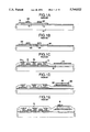
- FIGS. 1A-1E show an example for the steps of fabricating a circuit comprising a combination of an amorphous silicon diode and a crystalline silicon TFT in the prior art.
- An underlying insulation film 51 is formed on a glass substrate 50, over which an amorphous silicon film is formed and crystallized by applying long time annealing at a temperature higher than 600° C. Then, it is patterned to obtain an island-like silicon region 52. Then, a gate insulation film 53 is formed and, further, gate electrodes 54N and 54P are formed (refer to FIG. 1A).
- an N-type impurity region 55N and a p-type impurity region 55P are formed by using known CMOS fabrication technique.
- an impurity element is introduced into a semiconductor layer with a gate electrode as a mask in a self-aligning manner.
- the impurities are activated by laser annealing, heat annealing or like other means (refer to FIG. 1B).
- a first interlayer insulator 56 is formed through which contact holes are formed, thereby forming electrode/wiring 57a, 57b, 57c for source and drain of TFT, and an electrode 57d for an amorphous silicon diode (FIG. 1C).
- p-, I- (intrinsic) and N-type amorphous silicon films 58P, 58I and 58N are successively laminated, which are then patterned to form a diode junction portion (FIG. 1D).
- a second interlayer insulator 59 is formed through which contact holes are formed thereby forming an electrode 60 of the amorphous silicon diode to complete a circuit (FIG. 1E).
- crystallization of the silicon film used in the crystalline silicon TFT also requires a temperature higher than 600° C. and needs a time as much as 24 hours or longer for crystallization, many facilities for crystallization apparatus are required in actual mass production, which results in enormous installation cost.
- An object of the present invention is to provide a technique capable of overcoming the foregoing problems by simultaneously forming a semiconductor layer to form a TFT and a TFD using only a single interlayer insulator, as well as crystallizing the silicon film at a temperature lower than 600° C. and in such a short period of time as causing no substantial problems.
- Another object of the present invention is to provide a method capable of simplifying production processes and saving the number of film-forming steps.
- a further object of the present invention is to improve crystallization and activation of amorphous silicon, in particular, in an impurity region of TFT and TFD (source, drain or n-type or p-type region), thereby lowering the resistivity.
- a further object of the present invention is to lower the resistivity in an impurity region by annealing at a lower temperature and for a shorter period of time.
- a further object of the present invention is to obtain crystalline silicon by low temperature and short time annealing and then using the same to TFT.
- a further object of the present invention is to provide a semiconductor circuit in which source, drain of TFT and N-type and p-type regions of TFD are constituted with crystalline silicon, while an active region (channel forming region) of TFT and an I-layer of TFD is constituted with amorphous silicon, as well as a manufacturing method therefor.
- a further object of the present invention is to provide a semiconductor circuit in which the source, drain regions of TFT are constituted with crystalline silicon, while an active region of TFT and TFD are constituted with amorphous silicon, as well as a manufacturing method thereof.
- a further object of the present invention is to provide a semiconductor circuit, in which an active region of a TFT is constituted with crystalline silicon, while an intrinsic region of a TFD is constituted with amorphous silicon, as well as manufacturing method therefor.
- a further object of the present invention is to provide a semiconductor device/circuit in which TFT and/or TFD are formed from one semiconductor film, as well as a manufacturing method thereof.
- a further object of the present invention is to provide a method of manufacturing a semiconductor device/circuit capable of attaining a satisfactory light sensitivity.
- a further object of the present invention is to provide a method of manufacturing a semiconductor device/circuit capable of crystallizing an active region not introduced with a catalyst element by laterally proceeding crystallization.
- a further object of the present invention is to provide a method of manufacturing a semiconductor device/circuit capable of optionally fabricating a crystalline semiconductor region, and an amorphous semiconductor region.
- a further object of the present invention is to provide a semiconductor device/circuit containing TFT of extremely high mobility.
- the primary feature of the present invention is to add a catalytic element to a selected portion of a semiconductor film for reducing the crystallization temperature in the selected portion and to subject the semiconductor film to a heat annealing at such a temperature which is enough high to crystallize the impurity added portion but not enough high to crystallize the remaining portion of the semiconductor film, thereby, crystallizing only the selected portion of the semiconductor film.
- the foregoing problems can be solved by proceeding crystallization and activation thereby lowering the resistivity of amorphous silicon, particularly, in impurity regions (source, drain regions or n-type and p-type regions), of TFT and/or TFD.
- crystallization can be promoted by adding a trace amount of a catalyst material to a silicon film in a substantially amorphous state thereby enabling to lower the crystallization temperature and shorten the crystallization time.
- the amorphous state and the substantially amorphous state include a so-called amorphous state and an extremely degraded crystalline state if it is present.
- nickel (Ni), iron (Fe), cobalt (Co) or platinum (Pt) is suitable.
- crystallization can be attained by forming a film, particles, cluster or the like containing such a catalyst in the form of elemental metal or a compound such as silicide in an intimate contact on or below an amorphous silicon film or introducing such a catalyst element into the amorphous silicon film by an ion implantation or like other method and, subsequently, applying heat annealing at an appropriate temperature, typically, at a temperature below 580° C.
- the crystallization time is shorter as the annealing temperature is higher. Further, there is also a relation that the crystallization temperature is lower and the crystallization time is shorter as the concentration of the catalyst element is greater. According to the study of the present inventor, it has been found that at least one of the elements has to be present at a concentration of higher than 1 ⁇ 10 17 cm -3 , preferably, 5 ⁇ 10 18 cm -3 . Also, depending upon the annealing temperature and period, the catalytic element diffuses by 10-20 ⁇ m and the crystallization proceeds in a lateral direction.
- the concentration of the catalyst material does not exceed 2 ⁇ 10 20 cm -3 , preferably, 1 ⁇ 10 20 cm -3 in total in order to attain sufficient reliability and characteristic, particularly, when it is utilized as an active region. It has been found on the other hand that there is no substantial problem in the source or drain region if the catalyst is present relatively in a large amount. Particularly, it has been found that the concentration of the catalyst element contained in the active region (channel-forming region) of TFT is desirably smaller by more than one digit as that in the source; drain regions in the first feature of the present invention. In the same way, it is also desired in TFD that the concentration of the catalyst element contained in the intrinsic region (I-layer) is lower by more than one digit than that in the impurity region (n-type or p-type region).
- the amorphous state can be maintained without proceeding crystallization at all in such a region that the catalyst material is not present.
- crystallization of amorphous silicon not having such a catalyst material usually starts at a temperature higher than 600° C. but it does not proceed at all at a temperature lower than 580° C.
- hydrogen necessary for neutralizing dangling bonds in amorphous silicon is dissociated, in an atmosphere at a temperature higher than 300° C., it is desirable that annealing is applied in a hydrogen atmosphere in order to attain a satisfactory light sensitivity.
- such a catalyst element has an effect of crystallizing a peripheral area by diffusion during annealing. For instance, when annealing is applied at 550° C. for four hours, the catalyst element diffuses to the periphery as far as by 10-20 ⁇ m to cause crystallization therein. Accordingly, if the width of the gate electrode of TFT is less than 20 ⁇ m, preferably, less than 10 ⁇ m, crystallization proceeds laterally, and an active region (channel-forming region) not introduced with the catalyst element can also be crystallized by introducing the catalyst element into the source, drain regions before or after introduction of the n-type or p-type impurities and then applying annealing.
- the concentration of the catalyst element in the active region is generally low as compared with the concentration of the catalyst element in the source, drain regions.
- the lateral crystallization depends on the temperature and the time of annealing and the concentration of the catalyst element. Accordingly, the crystalline silicon region and the amorphous silicon region can be prepared optionally by optimizing them.
- the present inventor has succeeded in lowering the resistivity in the impurity region by low temperature and short time annealing thereby obtaining crystalline silicon and using it for TFT.
- the impurity region is crystallized and activated by taking an advantageous feature of the crystallization due to the catalyst material while the active region of TFT and the intrinsic region of TFD are left as they are in the amorphous state, thereby improving the function of the device.
- the present inventor has made a further study and has found a method capable of simplifying the process, that is, saving the number of film-forming steps as other object described above. The outline of the method is shown below.
- the impurity region of TFT is crystallized and activated by taking an advantageous feature of the crystallization due to the catalyst material while TFD is left as it is in the amorphous state thereby improving the function of the device.
- the present inventor has made a further study and has found a method capable of simplifying the process, that is, saving the number of film-forming steps as other object described above. The outline of the method is shown below.
- the TFT is crystallized and activated by taking an advantageous feature of crystallization due to the catalyst material while TFD is left as it is in the amorphous state thereby improving the function of the device.
- the present inventor has made a further study and found a method capable of simplifying the process, that is, saving the number of film-forming steps as other object described above. The outline of the method is shown below.
- the present inventor has found a method capable of simplifying the process, that is, saving the number of film-forming steps as the object described above by crystallizing and activating the impurity regions and the active region of TFT and the intrinsic region of TFD at a temperature lower than that in the prior art.
- the outline is shown below.
- catalyst element for example, by ion implantation or ion doping method
- catalyst element-containing material in the form of a film may be provided on a silicon film
- catalyst element for example, by ion implantation or ion doping method
- catalyst element-containing material in the form of a film may be provided on a silicon film
- the sequence for the steps of introducing the doping impurity and the catalyst element conducted one after the other can be reversed.
- the ion implantation or like other means is desirable for the step of introducing the catalyst element. Since the catalyst element is present, the annealing temperature lower than 600° C., typically, lower than 550° C. is sufficient for crystallization and activation, as well as the annealing time within 8 hours, typically, within 4 hours is sufficient.
- the catalyst element is distributed homogeneously by the ion implantation or ion doping method, crystallization proceeded extremely readily.
- the catalyst element is not brought into intimate contact with or implanted into the active region directly in the step for introducing the catalyst element (such as step (4') in the first and the second features of the invention). Accordingly, characteristics of the active region and the intrinsic region are not deteriorated.
- the TFD in the prior art has a laminate structure, whereas the present invention has a feature of a planar structure.
- the active region of TFT and the intrinsic region of TFD start from an identical amorphous silicon film.
- the catalyst element is not introduced in the TFD region, the region is not crystallized by the subsequent annealing step. This is attained since the annealing temperature in the present invention can be lowered by more than 50° C. than that in the prior art. Therefore, although two layers of silicon films have to be formed in the prior art, it is suffice to form a single silicon film layer in the present invention.
- the n-type layer and the p-type layer necessary so far can be obtained by forming them simultaneously in a planar structure upon doping impurities in TFT. That is, the n-type region of TFD is formed upon implantation of n-type impurities to TFT, while the p-type region of TFD is formed upon implantation of p-type impurities to TFT.
- the interlayer insulator can also be a single layer.
- Such a planar TFD has a novel feature not obtainable in the prior art.
- a conventional TFD having a shape as shown in FIG. 1
- the direction of an electric field generated at the inside of the semiconductor is vertical to a light irradiation plane, so that the light irradiation intensity is not uniform in the direction of the electric field and it has been impossible to efficiently generate electrons and holes and take out them externally.
- short-circuit may be caused sometimes to TFD due to pinholes through the layers.
- the direction of the electric field generated in TFD is in parallel with the light irradiation plane, the light intensity is constant in the direction of the electric field to improve photoelectric conversion efficiency and, in addition, suppress occurrence of short-circuit.
- a thin amorphous silicon film with a thickness of less than 1,000 ⁇ which is not crystallized by usual heat annealing, is also crystallized due to the effect of the catalyst element. It has been required that the thickness of the crystalline silicon film is less than 1,000 ⁇ , preferably, less than 500 ⁇ with a view point of avoiding pinholes or insulation failure in the gate insulation film and disconnection -of the gate electrode at stepped portions of TFT. This can not be attained so far by the method other than laser crystallization but this can be attained in accordance with the present invention by heat annealing even at a low temperature. This is naturally attributable to further improvement of the yield. In addition, in a case of utilizing TFD as a light sensor, S/N ratio and photoelectric conversion efficiency can be improved by using a thin semiconductor film.
- the present invention it is possible to save the number of processing steps for fabricating a semiconductor device/circuit having, for example, crystalline silicon TFT and amorphous silicon TFD and improving the productivity. Further, in the present invention, throughput can be improved also by crystallizing silicon, for example, at a temperature as low as 500° C. and at a processing time as short as four hours. In addition, in a case of adopting a process at a temperature higher than 600° C. in the prior art, there has been a problem of causing shrinkage or warp in a glass substrate which leads to the reduction of the yield, whereas such problems can be overcome altogether by utilizing the present invention.
- the present invention is of an industrial advantage.
- FIGS. 1A-E are cross sectional views illustrating an example of fabrication steps in the prior art
- FIGS. 2A-F are cross sectional views illustrating fabrication steps in Example 1 of the first feature of the present invention.
- FIGS. 3A-F are cross sectional views illustrating fabrication steps in Example 2 of the first feature of the present invention.
- FIGS. 4A-E are cross sectional views illustrating fabrication steps in Example 3 of the second feature of the present invention.
- FIGS. 5A-F are cross sectional views illustrating fabrication steps in Example 4 of the second feature of the present invention.
- FIGS. 6A-E are cross sectional views illustrating fabrication steps in Example 5 of the third feature of the present invention.
- FIGS. 7A-F are cross sectional views illustrating fabrication steps in Example 6 of the third feature of the present invention.
- FIGS. 8A-F are cross sectional views illustrating fabrication steps in Example 7 of the fourth feature of the present invention.
- FIG. 9A is a cross sectional view of a TFD obtained in the previous example.
- FIG. 9B is a band diagram of the TFD
- FIG. 9C is a cross sectional view illustrating a modified embodiment of the TFD.
- FIGS. 10A-F are cross sectional views illustrating fabrication steps in Example 8 of the fourth feature of the present invention.
- FIGS. 2A-F illustrate cross sectional views for fabrication steps in Example 1 of the first feature according to the present invention.
- an underlying film 11 made of silicon oxide was formed to a thickness of 2,000 ⁇ by a sputtering method on a substrate (Corning (Trademark) 7059) 10.
- an intrinsic (I) amorphous silicon film wasdeposited to a thickness of 500 to 1,500 ⁇ , for example, 1,500 ⁇ bya plasma CVD process.
- the thus obtained amorphous silicon film was patterned by photolithography to form an island-like silicon regions 14a (for TFT) and 14b (for TFD).
- a silicon oxide film 15 was deposited to a thickness of 1,000 ⁇ as a gate insulation film by a sputtering method.
- Sputtering was applied using silicon oxide as a target,at a substrate temperature of 200° to 400° C., for example, at 250° C. in a sputtering atmosphere of oxygen and argon at an argon/oxygen ratio of 0 to 0.5, for example, less than 0.1.
- a silicon film (containing 0.1 to 2% phosphorus) was deposited to a thickness of 6,000 to 8,000 ⁇ , for example, 6,000 ⁇ by a vacuum CVD process.
- the steps of forming the silicon oxide and the silicon film are desirably conducted continuously.
- the silicon film was patternedto form gate electrodes 16a and 16b for TFT and a mask material 16c for TFD(FIG. 2A).
- a photoresist mask 17a was formed and impurities(phosphorus) were implanted into the silicon region by plasma doping using the gate electrode as a mask.
- Doping was conducted by using phosphine (PH 3 3) as a doping gas at an acceleration voltage of 60 to 90 kV, for example, 80 kV.
- the amount of dose was 1 ⁇ 10 15 to 8 ⁇ 10 15 cm -2 , for example, 2 ⁇ 10 15 cm -2 .
- an N-type impurity region 18a for TFT and an N-type impurity region 19n for TFD were formed (FIG. 2B).
- nickel ions were implanted by an ion implantation method while leaving the photoresist mask 17a as it was.
- the amount of dose was 1 ⁇ 10 13 to 5 ⁇ 10 14 cm -2 , for example, 5 ⁇ 10 13 cm -2 .
- nickel was implanted ata concentration of about 5 ⁇ 10 18 cm -3 in the amorphous silicon film (FIG. 2C).
- a photoresist mask 17b was formed and impurities(boron) were implanted into the silicon region by plasma doping using the gate electrode as a mask.
- Diborane (B 2 H 6 ) was used as a doping gas and the acceleration voltage was 40 to 80 KV, for example, 65 KV.
- the amount of dose was 1 ⁇ 10 15 -8 ⁇ 10 15 cm -2 , for example, 5 ⁇ 10 15 cm -2 .
- a P-type impurity region 18b for TFT and a p-type impurity region 19p for TFD were formed.
- nickel was doped by using the photoresist mask 17b like that in FIG. 2C although not shown.
- the impurities were not implanted in a region interposed between the N-type region and the P-type region of TFD and the region became an intrinsic region 19i (FIG. 2D).
- a silicon oxide film 20 of 6,000 ⁇ thickness was formed as an interlayer insulator by plasma CVD, through which contact holes wereformed and electrode/wiring 21a, 21b, 21c for TFT and electrode/wiring 21d,21e for TFD were formed with a multi-layered film of metal material, for example, titanium or aluminum.
- annealing was applied in a hydrogen atmosphere at 1 atm at 350° C. for 30 min. A semiconductorcircuit was completed by the steps described above.
- the source, drain regions for the TFT of the completed semiconductor circuit were crystalline state and the channel region (active region) for TFT of the same was amorphous state.
- the P-type and N-type regions for the TFD of the same were crystalline state and the intrinsic region for TFD of the same was amorphous state.
- both of the silicon film and the interlayer insulator 20 could be a single layer. As a result, the number of film-forming steps was greatly reduced. Further, when the nickelconcentration in the active region for TFT and the intrinsic region for TFD was measured by secondary ion mass spectroscopy (SIMS), both of them were less than the measuring limit (1 ⁇ 10 16 cm -3 ). On the other hand, in the impurity regions for TFT and TFD, nickel at 1 ⁇ 10 18 to 5 ⁇ 10 18 cm -3 was detected.
- SIMS secondary ion mass spectroscopy
- FIGS. 3A-F illustrate cross sectional views for fabrication steps in Example 2 in the first feature of the present invention.
- a substrate Corning 7059
- the amorphous silicon film was patterned to formisland-like silicon regions 36a (for TFT) and 36b (for TFD).
- a silicon oxide film 37 of 1,000 ⁇ thickness was formed as a gate insulation film by plasma CVD using tetraethoxysilane (Si(OC 2 H 5 ) 4 , TEOS) and oxygen as the raw material.
- trichloroethylene C 2 HCl 3
- oxygen was caused to flow in a chamber at 400 SCCM and a plasma was generated at a substrate temperature of 300° C., total pressure of 5 Pa and an RF power of 150 W and this condition was kept for 10 min.
- a silicon oxide film was formed by introducing oxygen at 300 SCCM, TEOS at 15 SCCM and trichloroethylene at 2 SCCM to the chamber.
- the substrate temperature,the RF power and the total pressure were, respectively, 300° C., 75 W and 5 Pa.
- hydrogen at 100 Torr was introduced into the chamber and hydrogen annealing was applied at350° C. for 35 min.
- a tantalum film was deposited to a thickness of 6,000 to 8,000 ⁇ , for example, 6,000 ⁇ by sputtering. It is preferred that the film forming steps for the silicon oxide 37 and the tantalum film are conducted continuously. Instead of tantalum, chromium, molybdenum, tungsten, titanium or the like may also be used so long as it can endure the subsequent thermal annealing step. Then, the tantalum film was patterned to form gate electrodes 38a, 38b for TFT and a mask material 38cfor TFD. Further, the surface of the tantalum wiring was anodized to form an oxide layer on the surface. Anodization was conducted in a solution of 1-5% tartaric acid in ethylene glycol. The thickness of the resultant oxide layer was 2,000 ⁇ (FIG. 3A).
- impurities phosphorus
- Phosphine PH 3
- the acceleration voltage was 60 to 90 kV, for example, 80 kV.
- the amount of dose was 1 ⁇ 10 15 -8 ⁇ 10 15 cm -2 , for example, 2 ⁇ 10 15 cm -2 .
- an N-type impurity region 39 wasformed (FIG. 3B).
- nickel ions were implanted by ion implantation.
- the amount ofdose was 1 ⁇ 10 13 to 5 ⁇ 10 14 cm -2 , for example, 5 ⁇ 10 13 cm -2 .
- nickel was implanted in the amorphous silicon film at a concentration of about 5 ⁇ 10 18 cm -3 (FIG. 3C).
- impurities boron
- Diborane (B 2 H 6 ) was used as thedoping gas and the acceleration voltage was 50-80 kV, for example, 65 kV.
- the amount of dose was 1 ⁇ 10 15 to 8 ⁇ 10 15 cm -2 , for example, at 5 ⁇ 10 15 cm -2 which is greater than the amount of phosphorus implanted previously.
- an N-type impurityregion 41a, a p-type impurity region 41b for TFT and an N-type region 42n and p-type region 42p for TFD were formed (FIG. 3D).
- the impurities were activated by annealing in a reducing hydrogen atmosphere at 0.1 to 1 atm, at 500° C. for 4 hours.
- a reducing hydrogen atmosphere at 0.1 to 1 atm, at 500° C. for 4 hours.
- nickel since nickel was diffused in the regions 41a, 41b and 42p, 42n to which nickel was implanted previously, crystallization proceeded easilyin these regions at such a relatively low temperature.
- nickel since nickel was not present in the silicon of the active region for TFT and the intrinsic region 42i for TFD, the regions were not crystallized (FIG. 3E).
- a silicon oxide film 43 was formed to 2,000 ⁇ thickness as an interlayer insulator by plasma CVD through which contact holes were formed and electrode/wiring 44a, 44b and 44c for TFT and electrode/wiring 44d, 44e for TFD were formed with a multi-layered film ofmetal material, for example, titanium nitride and aluminum.
- This structure is advantageous in that the titanium nitride has a good electrical contactin contact with the source and drain regions.
- annealing was applied in a hydrogen atmosphere at 1 atm at 350° C. for 30 min. With the steps as described above, a semiconductor circuit was completed (FIG. 3F).
- the source, drain regions for TFT of the completed semiconductorcircuit were crystalline state and the channel region (active region) for TFT of the same was amorphous state.
- the P-type and N-type regions for TFDof the same were crystalline state and the intrinsic region for TFD of the same was amorphous state.
- FIGS. 4A-E illustrate cross sectional views for fabrication steps in Example 3 in the second feature of the present invention.
- Identical or similar element to those in Example 2 carry the same reference numerals.
- an underlying film 31 of silicon oxide to a thickness of 2,000 ⁇ by sputtering and, further, anamorphous silicon film by plasma CVD. Then, the amorphous silicon film was patterned to form island-like silicon regions 36a (for TFT) and 36b (for TFD).
- a silicon oxide film 37 of 1,000 ⁇ thickness was formedas a gate insulation film by plasma CVD using tetraethoxysilane (Si(OC 2 H 5 ) 4 , TEOS) and oxygen as the raw material.
- tetraethoxysilane Si(OC 2 H 5 ) 4 , TEOS
- oxygen was caused to flow in a chamber at 400 SCCM and a plasma was generated at a substrate temperature of 300° C., total pressure of 5 Pa and an RF power of 150 W and this condition was kept for 10 min.
- a silicon oxide film was formed by introducing oxygen at 300 SCCM, TEOS at 15 SCCM and trichloroethylene at 2 SCCM to the chamber.
- the substrate temperature, the RF power and the total pressure were, respectively, 300° C., 75 W and 5 Pa.
- hydrogen at 100 Torr was introduced into the chamber and hydrogen annealingwas applied at 350° C. for 35 min.
- a tantalum film was deposited to a thickness of 6,000 to 8,000 ⁇ , for example, 6,000 ⁇ by sputtering. It is preferred that the film forming steps for the silicon oxide 37 and the tantalum film are conducted continuously. Instead of tantalum, chromium, molybdenum, tungsten, titanium or the like may also be used so long as it can endure the subsequent annealing step. Then, the tantalum film was patterned to form gate electrodes 38a, 38b for TFT and a mask material 38c for TFD. Further, the surface of the tantalum wiring was anodized to form an oxide layer on the surface. Anodization was conducted in a solution of 1-5% tartaric acid in ethylene glycol. The thickness of the resultant oxide layer was 2,000 ⁇ (FIG. 4A).
- impurities phosphorus
- Phosphine PH 3
- the acceleration voltage was 60 to 90 kV, for example, 80 kV.
- the amount of dose was 1 ⁇ 10 15 -8 ⁇ 10 15 cm -2 , for example, 2 ⁇ 10 15 cm -2 .
- an N-type impurity region 39 wasformed (FIG. 4B).
- impurities boron
- Diborane B 2 H 6
- the accelerationvoltage was 50 to 80 kV, for example, 65 kV.
- the amount of dose was 1 ⁇ 10 15 to 8 ⁇ 10 15 cm -2 , for as example, at 5 ⁇ 10 15 cm -2 which is greater than the amount of phosphorusimplanted previously.
- an N-type impurity region 41a, a p-type impurity region 41b for TFT and an N-type region 42n and p-type region 42pfor TFD were formed (FIG. 4C).
- a mask 40b was formed by photoresist in the TFD region and nickel ions were implanted by ion implantation.
- the amount of dose was 1 ⁇ 10 13 to 5 ⁇ 10 14 cm -2 , for example, 5 ⁇ 10 13 cm -2 .
- nickel was implanted in the impurity regions 41a, 41b of TFT at a concentration of about 5 ⁇ 10 18 cm -3 (FIG. 4D).
- the impurities were activated by annealing in a reducing hydrogen atmosphere at 0.1 to 1 atm, at 500° C. for 4 hours.
- crystallization proceeded easily by this annealing to activate the doped impurities in the regions 41a, 41b to which nickel was implantedpreviously.
- nickel since nickel was not present in the silicon region for TFD, the region was not crystallized.
- a silicon oxide film 43 was formed to a 2,000 ⁇ thicknessas an interlayer insulator by plasma CVD through which contact holes were formed and electrode/wiring 44a, 44b, 44c for TFT and electrode/wiring 44d, 44e for TFD were formed with a multi-layered film of metal material, for example, titanium nitride and aluminum.
- annealing was appliedin a hydrogen atmosphere at 1 atm at 350° C. for 30 min. With the steps as described above, a semiconductor circuit was completed (FIG. 4E).
- the source, drain regions for TFT of the completed semiconductorcircuit were crystalline state and the channel region (active region) for TFT of the same was amorphous state or crystalline state due to diffused nickel from impurity region.
- the regions for TFD of the same were all amorphous state.
- FIGS. 5A-F illustrate cross sectional views for fabrication steps in Example 4 in the second feature of the present invention.
- Identical or similar elements to those in Example 2 carry the same reference numerals.
- an underlying film 31 of silicon oxide was formed to a thickness of 2,000 ⁇ by sputtering.
- an amorphous silicon film 32 to a thickness of 500 to 1,500 ⁇ , for example, 500 ⁇ and a silicon oxide film 33 to a thickness of 200 ⁇ by plasma CVD.
- the amorphous silicon film 32 was maskedwith a photoresist 34, and nickel ions were selectively implanted by an ionimplantation method to prepare a region 35 in which nickel was contained by1 ⁇ 10 18 to 2 ⁇ 10 19 cm -3 , for example, 5 ⁇ 10 18 cm -3 .
- the thickness of the region 35 was made to 200 to 500 ⁇ , and an optimumacceleration energy was selected correspondingly. Further, nickel was not implanted in the region to form a channel-forming region in TFT and a region to fabricate TFD.
- the channel length of TFT was set to less than 20 ⁇ m, preferably, 10 ⁇ m, because nickel can be diffused by annealing to crystallize the channel forming region. By utilizing this effect, crystallization can be promoted while lowering the nickel concentration inthe active region of TFT (FIG. 5A).
- amorphous silicon film was patterned to form island-like silicon regions 36a (for TFT) and 36b (for TFD). Further, a silicon oxide film 37 of 1,000 ⁇ thickness was formed as a gate insulation film by plasma CVD using tetraethoxysilane (Si(OC 2 H 5 ) 4 , TEOS) and oxygen as the raw material.
- trichloroethylene C 2 HCl 3
- oxygen was caused to flow in a chamber at 400 SCCM and plasmas were generated at a substrate temperature of 300° C., total pressure of 5 Pa and an RF power of 150 W and this condition was maintained for 10 min.
- a silicon oxide film was formed by introducing oxygen at 300SCCM, TEOS at 15 SCCM and trichloroethylene at 2 SCCM to the chamber.
- the substrate temperature, the RF power and the total pressure were, respectively, 300° C., 75 W and 5 Pa.
- hydrogen at 100 Torr was introduced into the chamber and hydrogen annealing was applied at 350° C. for 35 min.
- a tantalum film was deposited to a thickness of 6,000 to 8,000 ⁇ , for example, 6,000 ⁇ by sputtering. It is preferred that the film forming steps for the silicon oxide 37 and the tantalum film are conducted continuously. Instead of tantalum, chromium, molybdenum, tungsten, titanium or the like may also be used so long as it can endure the subsequent annealing step. Then, the tantalum film was patterned to form gate electrodes 38a, 38b for TFT and a mask material 38c for TFD. Further, the surface of the tantalum wiring was anodized to form an oxide layer on the surface. Anodization was conducted in a solution of 1-5% tartaric acid in ethylene glycol. The thickness of the resultant oxide layer was 2,000 ⁇ (FIG. 5B).
- impurities phosphorus
- Phosphine PH 3
- the acceleration voltage was 60 to 90 kV, for example, 80 kV.
- the amount of dose was 1 ⁇ 10 15 -8 ⁇ 10 15 cm -2 , for example, 2 ⁇ 10 15 cm -2 .
- an N-type impurity region 39 wasformed (FIG. 5C).
- impurities boron
- Diborane B 2 H 6
- the accelerationvoltage was 50 to 80 kV, for example, 65 kV.
- the amount of dose was 1 ⁇ 10 15 to 8 ⁇ 10 15 cm -2 , for example, at 5 ⁇ 10 15 cm -2 which was greater than the amount of phosphorus implanted previously.
- an N-type impurity region 41a, a p-type impurity region 41b for TFT and an N-type region 42n and a p-type region 42p for TFD were formed (FIG. 5D).
- the impurities were activated by annealing in a reducing hydrogen atmosphere at 0.1 to 1 atm, at 500° C. for 4 hours.
- crystallization proceeded easily by this annealing to activate the doped impurities in the region 36a to which nickel was implanted previously.
- nickel since nickel was not present in the siliconof the region 36b (including intrinsic region 42i) for TFD, the region was not crystallized (FIG. 5E).
- a silicon oxide film 43 was formed to a 2,000 ⁇ thicknessas an interlayer insulator by plasma CVD through which contact holes were formed and electrode/wiring 44a, 44b, 44c for TFT and electrode/wiring 44d, 44e for TFD were formed with a multi-layered film of metal material, for example, titanium nitride and aluminum.
- annealing was appliedin a hydrogen atmosphere at 1 atm at 350° C. for 30 min. With the steps as described above, a semiconductor circuit was completed (FIG. 5F).
- the source, drain regions for TFT of the completed semiconductordevice were crystalline state and the regions for TFD of the same were all amorphous state. Also, the channel region of the TFT could be crystallizedbecause of the nickel diffused from the source and drain regions.
- FIGS. 6A-E illustrates cross sectional views for fabrication steps in Example 5 of the third feature according to the present invention.
- Identical or similar elements to those in Example 1 carry the same reference numerals.
- an underlying film 11 made of silicon oxide was formed to a thickness of 2,000 ⁇ by a sputtering method on a substrate (Corning 7059) 10.
- an intrinsic (I) amorphous silicon film was deposited to a thickness of 500 to 1,500 ⁇ , for example, 1,500 ⁇ by plasma CVD.
- the thus obtained amorphous silicon film was patterned by photolithography to form an island-like silicon regions 14a (for TFT) and 14b (for TFD).
- a silicon oxide film 15 was deposited to a thickness of 1,000 ⁇ as a gate insulation film by a sputtering method.
- Sputtering was applied using silicon oxide as a target,at a substrate temperature of 200° to 400° C., for example, at 250° C. in a sputtering atmosphere of oxygen and argon at an argon/oxygen ratio of 0 to 0.5, for example, less than 0.1.
- a silicon film (containing 0.1 to 2% phosphorus) was deposited to a thickness of 6,000 to 8,000 ⁇ , for example, 6,000 ⁇ by vacuum CVD. The steps of forming the silicon oxide and the silicon film are desirably conducted continuously.
- the silicon film was patterned to form gate electrodes 16a and 16b for TFT and a mask material 16c for TFT (FIG. 6A).
- a photoresist mask 17a was formed and impurities(phosphorus) were implanted into the silicon region by plasma doping using the gate electrode as a mask.
- Doping was conducted by using phosphine (PH 3 ) as a doping gas at an acceleration voltage of 60 to 90 kV, for example, 80 kV.
- the amount of dose was 1 ⁇ 10 15 to 8 ⁇ 10 15 cm -2 , for example, 2 ⁇ 10 15 cm -2 .
- an N-type impurity region 18a for TFT and an N-type impurity region 19n for TFD were formed (FIG. 6B).
- a photoresist mask 17b was formed and impurities(boron) were implanted into the silicon region by plasma doping using the gate electrode as a mask.
- Diborane (B 2 H 6 ) was used as a doping gas and the acceleration voltage was 40 to 80 KV, for example, 65 KV.
- the amount of dose was 1 ⁇ 10 15 -8 ⁇ 10 15 cm -2 , for example, 5 ⁇ 10 15 .
- a p-type impurity region 18b for TFT and a p-type impurity region 19p for TFD were formed.
- the impurities were not implanted in a region interposed between the N-type region and the p-type region of TFD by the mask material 16c of TFD and the region became an intrinsic region 19i. After introducing impurities, the mask material 16c for TFD was removed (FIG. 6C).
- a photoresist mask 17c was formed covering the TFD region and nickel ions were implanted by an ion implantation method by using this mask.
- the amount of dose was 1 ⁇ 10 13 to 5 ⁇ 10 14 cm -2 , for example, 5 ⁇ 10 13 cm -2 .
- nickel was implanted at a concentration of about 5 ⁇ 10 18 cm -3 in the impurity regions 18a, 18b of the TFT region (FIG. 6D).
- impurities were activated by annealing in a reducing hydrogenatmosphere at 0.1 to 1 atm at 500° C. for 4 hours.
- nickel since nickel was diffused in the regions 18a, 18b to which nickel was previously implanted, crystallization proceeded easily by this annealing and the doped impurities were activated.
- the width of the gateelectrode is less than 20 ⁇ m, preferably, less than 10 ⁇ m, nickel diffused from the impurity region to proceed crystallization as far as theactive region.
- nickel since nickel was not present in silicon region of TFD, no crystallization occurred.
- a silicon oxide film 20 of 6,000 ⁇ thickness was formed as an interlayer insulator by plasma CVD, through which contact holes wereformed and electrode/wiring 21a, 21b, 21c for TFT and electrode/wiring 21d,21e for TFD were formed with a multi-layered film of metal material, for example, titanium nitride or aluminum.
- annealing was applied in ahydrogen atmosphere at 1 atm at 350° C. for 30 min.
- a semiconductor circuit was completed by the steps described above (FIG. 6E).
- the source, drain regions for TFT of the completed semiconductorcircuit were crystalline state and TFD of the same was amorphous state.
- both of the silicon film and the interlayer insulator 20 could be a single layer. As a result, the number of film-forming steps was greatly reduced. Further, when the nickelconcentration was measured by secondary ion mass spectroscopy (-SIMS), nickel at 1 ⁇ 10 18 -5 ⁇ 10 18 cm -3 was detected in the impurity region of TFT. On the other hand, in the region for TFD, it was less than the measuring limit (1 ⁇ 10 16 cm -3 ).
- FIGS. 7A-E illustrates cross sectional views for fabrication steps in Example 6 of the third feature according to the present invention.
- Identical or similar elements to those in Example 1 carry the same reference numerals.
- an underlying film 11 made of silicon oxide was formed to a thickness of 2,000 ⁇ by a sputtering method on a substrate (Corning 7059) 10.
- an intrinsic (I) amorphous silicon film 12 was deposited to a thickness of 500 to 1,500 ⁇ , for example, 1,500 ⁇ by plasma CVD.
- the film was crystallized by annealing in a reducing hydrogen atmosphere (preferably, 0.1-1 atm of hydrogen partial pressure), at 500° C. for 4 hours.
- a reducing hydrogen atmosphere preferably, 0.1-1 atm of hydrogen partial pressure
- the amorphous silicon film below the nickel silicide film 13 was crystallized into a crystalline silicon film.
- the silicon film in the region in which the nickel silicide film was not present remained in the amorphous state as itwas.
- amorphous silicon film was patterned by photolithography to form an island-like silicon regions 14a (for TFT) and 14b (for TFD). While the region 14a was crystallized in the previous annealing step, the region 14b remained amorphous as it was. Further, a silicon oxide film 15 was deposited to a thickness of 1,000 ⁇ as a gate insulation film by sputtering. Sputtering was applied using silicon oxide as a target, at a substrate temperature of 200° to 400° C., for example, at 300° C. in a sputtering atmosphere of oxygen and argon at an argon/oxygen ratio of 0 to 0.5, for example, less than 0.1.
- a silicon film (containing 0.1 to 2% phosphorus) was deposited to a thickness of 6,000 to 8,000 ⁇ , for example, 6,000 ⁇ by vacuum CVD.
- the steps of forming the silicon oxideand the silicon film are desirably conducted continuously.
- the silicon film was patterned to form gate electrodes 16a and 16b for TFT and a mask material 16c for TFD (FIG. 7B).
- a photoresist mask 17a was formed and impurities(phosphorus) were implanted into the silicon region by plasma doping using the gate electrode as a mask.
- Doping was conducted by using phosphine (PH 3 ) as a doping gas at an acceleration voltage of 60 to 90 kV, for example, 80 kV.
- the amount of dose was 1 ⁇ 10 15 to 8 ⁇ 10 15 cm -2 , for example, 2 ⁇ 10 15 cm -2 .
- an N-type impurity region 18a for TFT and an N-type impurity region 19n for TFD were formed (FIG. 7C).
- a photoresist mask 17b was formed and impurities(boron) were implanted into the silicon region by plasma doping using the gate electrode as a mask.
- Diborane (B 2 H 6 ) was used as a doping gas and the acceleration voltage was 40 to 80 KV, for example, 65 KV.
- the amount of dose was 1 ⁇ 10 15 to 8 ⁇ 10 15 cm -2 , for example, 5 ⁇ 10 15 cm -2 .
- a P-type impurity region 18b for TFT and a P-type impurity region 19p for TFD were formed.
- the impurities were not implanted in a region interposed between the n-type region and the p-type region of TFD by the mask 16c of TFD and the region became an intrinsic region 19i (FIG. 7D).
- a silicon oxide film 20 of 6,000 ⁇ thickness was formed as an interlayer insulator by plasma CVD, through which contact holes wereformed and electrode/wiring 21a, 21b, 21c for TFT and electrode/wiring 21d,21e for TFD were formed with a multi-layered film of metal material, for example, titanium nitride and aluminum.
- annealing was applied in a hydrogen atmosphere at 1 atm at 350° C. for 30 min.
- a semiconductor circuit was completed by the steps described above (FIG. 7F).
- the regions for TFT of the completed semiconductor circuit were all crystalline state and the regions for TFD were all amorphous state.
- both of the silicon film 12 and the interlayer insulator 20 could be a single layer. As a result, the number of film-forming steps was greatly reduced. Further, when the nickelconcentration was measured by secondary ion mass spectroscopy (SIMS), nickel at 1 ⁇ 10 18 to 5 ⁇ 10 18 cm -3 was detected inthe region 14a for TFT. On the other hand, it was less than the measuring limit (1 ⁇ 10 16 cm -3 ) in the region 14b for TFD.
- SIMS secondary ion mass spectroscopy
- FIGS. 8A-F illustrate cross sectional views for fabrication steps in Example 7 of the fourth feature according to the present invention.
- Identical or similar elements to those in Example 1 carry the same reference numerals.
- an underlying film 11 made of silicon oxide was formed to a thickness of 2,000 ⁇ by a sputtering method on a substrate (Corning 7059) 10.
- an intrinsic (I) amorphous silicon film 12 was deposited to a thickness of 500 to 1,500 ⁇ , for example, 1,500 ⁇ by a plasma CVD process.
- nickel ions were implanted to the thus obtained amorphous silicon film by an ion implantation method.
- the amount of dose was 1 ⁇ 10 13 to 5 ⁇ 10 14 cm -2 , for example, 5 ⁇ 10 13 cm -2 .
- nickel was implanted at a concentration of about 5 ⁇ 10 18 cm -3 in the amorphous silicon film (FIG. 8A).
- a silicon oxide film 15 was deposited to a thickness of 1,000 ⁇ as a gate insulation film by a sputtering method.
- Sputtering was applied using silicon oxide asa target, at a substrate temperature of 200° to 400° C., for example, at 250° C. in a sputtering atmosphere of oxygen and argon at an argon/oxygen ratio of 0 to 0.5, for example, less than 0.1.
- a silicon film (containing 0.1 to 2% phosphorus) was deposited to a thickness of 6,000 to 8,000 ⁇ , for example, 6,000 ⁇ by vacuum CVD.
- the steps of forming the silicon oxide and the silicon film are desirably conducted continuously.
- the silicon film was patternedto form gate electrodes 16a and 16b for TFT and a mask material 16c for TFD(FIG. 8B).
- a photoresist mask 17a was formed and impurities(phosphorus) were implanted into the silicon region by plasma doping using the gate electrode as a mask.
- Doping was conducted by using phosphine (PH 3 ) as a doping gas at an acceleration voltage of 60 to 90 kV, for example, 80 kV.
- the amount of dose was 1 ⁇ 10 15 to 8 ⁇ 10 15 cm -2 , for example, 2 ⁇ 10 15 cm -2 .
- an N-type impurity region 18a for TFT and an N-type impurity region 19n for TFD were formed (FIG. 8C).
- a photoresist mask 17b was formed and impurities(boron) were implanted into the silicon region by plasma doping using the gate electrode as a mask.
- Diborane (B 2 H 6 ) was used as a doping gas and the acceleration voltage was 40 to 80 KV, for example, 65 KV.
- the amount of dose was 1 ⁇ 10 15 to 8 ⁇ 10 15 cm -2 , for example, 5 ⁇ 10 15 cm -2 .
- a P-type impurity region 18b for TFT and a P-type impurity region 19p for TFD were formed.
- An intrinsic region 19i was left between the n-type region 19n and the p-type region 19p of TFD (FIG. 8D).
- a silicon oxide film 20 of 6,000 ⁇ thickness was formed as an interlayer insulator by plasma CVD, through which contact holes wereformed and electrode/wiring 21a, 21b, 21c for TFT and electrode/wiring 21d,21e for TFD were formed with a multi-layered film of metal material, for example, titanium nitride and aluminum.
- annealing was applied in a hydrogen atmosphere at 1 atm at 350° C. for 30 min.
- a semiconductor circuit was completed by the steps described above (FIG. 8F).
- both of the silicon film 12 and the interlayer insulator 20 could be a single layer. As a result, the number of film-forming steps was greatly reduced. Further, when the nickelconcentration in the active region of TFT and the intrinsic region of TFD was measured by secondary ion mass spectroscopy (SIMS), nickel at 1 ⁇ 10 18 to 5 ⁇ 10 18 cm -3 was detected in both of the cases.
- SIMS secondary ion mass spectroscopy
- FIG. 9A shows a portion of a semiconductor layer of the TFD in the semiconductor circuits of Examples 1, 5, 6 and 7.
- TFD When TFD is used as a light sensor, light enters from above through the passivation film 20.
- FIG. 9B shows an energy band diagram along line A-A' of TFD.
- the p-type region 19p and the n-type region 19n are crystalline silicon
- the intrinsic region 19i is amorphous silicon (for example Examples 1 or 2)
- band gaps for the p-type region and the n-type region (Ep, En) are smaller than the band gap Ei for the intrinsic region 19i and, therefore, i-n junction of the conduction band and the p-ijunction of the valance band are abrupt and the electron-hole pairs caused by irradiation of light are separated rapidly. As a result, photoelectric conversion efficiency is increased.
- the photosensitivity of crystalline silicon is generally low, and this may be improved, as shown in FIG. 9C, by removing the mask 16c of the TFD and then forming a semiconductor film 19a of a high photosensitivity such as hydrogenated amorphous silicon at a thickness of 1,000 to 8,000 ⁇ , for example, 3,000 ⁇ in an intimate contact with the intrinsic region 19i.
- a high photosensitivity such as hydrogenated amorphous silicon
- carriers are generated in the amorphous semiconductor film 19a and, at the same time, carriers are generated also in the crystalline silicon semiconductor film 19i in accordance with the dependence of the light sensitivity on the wavelength. Accordingingly, it is possible to convert a light in a wider wavelength regioninto electricity.
- carbon, nitrogen, oxygen or the like maybe added thereto for changing the dependence of the light sensitivity on the wavelength.
- the energy band width of the amorphous semiconductor film 19a is broaderas compared with that of the intrinsic region 19i, the carriers generated in the intrinsic region 19i are prevented from drifting to the amorphous semiconductor film 19a, and the carriers generated in the amorphous semiconductor film 19a move along the slope of the energy band to the intrinsic region 19i. Accordingly, the generated carriers can be taken outexternally more efficiently.
- FIGS. 10A-F illustrate cross sectional views for fabrication steps in Example 8 of the fourth feature of the present invention.
- Identical or similar elements to those in Example 2 carry the same reference numerals.
- an underlying film 31 of silicon oxide to a thickness of 2,000 ⁇ by sputtering and, further, anamorphous silicon film by plasma CVD. Then, the amorphous silicon film was patterned to form island-like silicon regions 36a (for TFT) and 36b (for TFD).
- a silicon oxide film 37 of 1,000 ⁇ thickness was formedas a gate insulation film by plasma CVD using tetraethoxysilane (Si(OC 2 H 5 ) 4 , TEOS) and oxygen as the raw material.
- tetraethoxysilane Si(OC 2 H 5 ) 4 , TEOS
- oxygen was caused to flow in a chamber at 400 SCCM and a plasma was generated at a substrate temperature of 300° C., total pressure of 5 Pa and an RF power of 150 W and this condition was maintained for 10 min.
- a silicon oxide film was formed by introducing oxygen at 300 SCCM, TEOS at 15 SCCM and trichloroethylene at 2 SCCM to the chamber.
- the substrate temperature, the RF power and the total pressure were, respectively, 300° C., 75 W and 5 Pa.
- hydrogen at 100 Torr was introduced into the chamber and hydrogen annealingwas applied at 350° C. for 35 min.
- the surface of the tantalum wiring was anodized to form an oxide layer on the surface.
- Anodization was conducted in a solution of 1-5% tartaric acid in ethylene glycol.
- the thickness of the resultant oxide layer was 2,000 ⁇ (FIG. 10A).
- impurities phosphorus
- Phosphine PH 3
- the acceleration voltage was 60 to 90 kV, for example, 80 kV.
- the amount of dose was 1 ⁇ 10 15 -8 ⁇ 10 15 cm -2 , for example, 2 ⁇ 10 15 cm -2 .
- an N-type impurity region 39 wasformed (FIG. 10B).
- nickel ions were implanted by ion implantation.
- the amount ofdose was 1 ⁇ 10 13 to 5 ⁇ 10 14 cm -2 , for example, 5 ⁇ 10 13 cm -2 .
- nickel was implanted in the amorphous silicon film for both of the TFTs and TFD at a concentration of about 5 ⁇ 10 18 cm -3 (FIG. 10C).
- impurities boron
- Diborane B 2 H 6
- the acceleration voltage was 50 to 80 kV, for example, 65 kV.
- the amount of dose was 1 ⁇ 10 15 to 8 ⁇ 10 15 cm -2 , for example, at 5 ⁇ 10 15 cm -2 which was greater than the amount of phosphorus implanted previously.
- an N-type impurity region 41a, a P-type impurity region 41b for TFTand an n-type region 42n and p-type region 42p for TFD were formed (FIG. 10D).
- the impurities were activated by annealing in a reducing hydrogen atmosphere at 0.1 to 1 atm, at 500° C. for 4 hours.
- nickel since nickel was diffused in the regions 41a, 41b and 42p, 42n to which nickel was implanted previously, crystallization proceeded easilyby this annealing to activate the doped impurities.
- Nickel was diffused also in the active region for TFT to proceed crystallization.
- nickel since nickel was not present in silicon, particularly, in a central portion of the intrinsic region 42i of TFD, and there was no diffusion from the periphery thereof, crystallization did not occur.
- TFT was crystallized over the entire area, while TFD was crystallized in the impurity region and a portion of intrinsic region in contact with the impurity region, whereas the central portion of the intrinsic region 42i remained amorphous (FIG. 10F).
- a silicon oxide film 43 was formed to 2,000 ⁇ thickness as an interlayer insulator by plasma CVD through which contact holes were formed and electrode/wiring 44a, 44b, 44c for TFT and electrode/wiring 44d, 44e for TFD were formed with a multi-layered film of metal material, for example, titanium nitride and aluminum. Finally, annealing was appliedin a hydrogen atmosphere at 1 atm at 350° C. for 30 min. With the steps as described above, a semiconductor circuit was completed (FIG. 10F).
- the mask material 38c of TFD is insulated from other gate electrode wirings and put to a floated potentialstate.
- TFD operation may sometimes be hindered by accumulation of some or other electric charges. If stable operation is required, it is preferred to put the mask at the same potential as that for the p-type region or the n-type region of TFD.
- the maskmaterial 38c is present on the intrinsic region 42i in these examples, it is necessary to enter light on the side of the substrate when TFD is used as a light sensor.
- Example 7 since an amorphous state portion having satisfactory light sensitivity is left in the intrinsic region 42i, there is no substantial problem.
- the channel forming region of the TFT in the examples ofthe present invention was taught to be intrinsic, the "intrinsic" in the present invention may include "N - " or "P - " type conductivity.
- the examples show only a PIN junction for the TFD, PP - N, PN - N junctions or the like may also be used.
Abstract
Amorphous silicon in impurity regions (source and drain regions or N-type or p-type regions) of TFT and TFD are crystallized and activated to lower electric resistance, by depositing film having a catalyst element such as nickel (Ni), iron (Fe), cobalt (Co) or platinum (Pt) on or beneath an amorphous silicon film, or introducing such a catalyst element into the amorphous silicon film by ion implantation and subsequently crystallizing the same by applying heat annealing at an appropriate temperature.
Description
This application is a Continuation of Ser. No. 08/483,048, filed Jun. 7, 1995, now abandoned; which itself is a divisional of Ser. No. 08/216,107, filed Mar. 21, 1994 (now U.S. Pat. No. 5,501,989).
1. Field of the Invention
The present invention relates to a semiconductor device/circuit having at least partially crystallized semiconductor layer and a manufacturing method thereof. The semiconductor device/circuit manufactured according to the present invention is formed on any of insulation substrates such as glass substrates and semiconductor substrates such as single crystal silicon substrates. In particular, the present invention relates to a semiconductor device/circuit having a thin film transistor (TFT) and/or a thin film diode (TFD) (for example, image sensor) manufactured by way of crystallization (activation) through heat annealing.
2. Description of the Prior Art
Thin film semiconductor devices such as TFT and TFD are classified into amorphous devices and crystalline devices depending on the crystalline structures of the semiconductor materials used. Amorphous silicon can be fabricated at a low temperature and shows excellent mass productivity. However, it is inferior to crystalline silicon in view of physical properties such as field effect mobility or conductivity. So it has been demanded for crystalline semiconductor devices in order to obtain high speed characteristics. On the other hand, it has been known that amorphous semiconductors are usable, for example, to light sensors since they generally show large change in the photoconductivity. It has been proposed recently a circuit for driving a light sensor using an amorphous silicon diode or a thin film diode by a thin film transistor using crystalline silicon capable of high speed operation (for example, integrated image sensor circuit).
FIGS. 1A-1E show an example for the steps of fabricating a circuit comprising a combination of an amorphous silicon diode and a crystalline silicon TFT in the prior art. An underlying insulation film 51 is formed on a glass substrate 50, over which an amorphous silicon film is formed and crystallized by applying long time annealing at a temperature higher than 600° C. Then, it is patterned to obtain an island-like silicon region 52. Then, a gate insulation film 53 is formed and, further, gate electrodes 54N and 54P are formed (refer to FIG. 1A).
Then, an N-type impurity region 55N and a p-type impurity region 55P are formed by using known CMOS fabrication technique. In this impurity introduction step, an impurity element is introduced into a semiconductor layer with a gate electrode as a mask in a self-aligning manner. After the implantation of impurities, the impurities are activated by laser annealing, heat annealing or like other means (refer to FIG. 1B).
Then, a first interlayer insulator 56 is formed through which contact holes are formed, thereby forming electrode/ wiring 57a, 57b, 57c for source and drain of TFT, and an electrode 57d for an amorphous silicon diode (FIG. 1C).
Then, p-, I- (intrinsic) and N-type amorphous silicon films 58P, 58I and 58N are successively laminated, which are then patterned to form a diode junction portion (FIG. 1D).
Finally, a second interlayer insulator 59 is formed through which contact holes are formed thereby forming an electrode 60 of the amorphous silicon diode to complete a circuit (FIG. 1E).
In the prior art method requiring such procedures, it is necessary to form silicon films 52, 58I and the interlayer insulators 56, 59 each by two layers, which requires film formation for long time and, in addition, the N-type layer 58N and the p-type layer 58P have to be formed. Therefore, it involves a problem that the throughput is reduced. Further, a plasma CVD or vacuum CVD process used for forming such films, takes much dead time for the maintenance of the apparatus and the presence of such additional step further reduces the throughput.
Furthermore, since crystallization of the silicon film used in the crystalline silicon TFT also requires a temperature higher than 600° C. and needs a time as much as 24 hours or longer for crystallization, many facilities for crystallization apparatus are required in actual mass production, which results in enormous installation cost.
An object of the present invention is to provide a technique capable of overcoming the foregoing problems by simultaneously forming a semiconductor layer to form a TFT and a TFD using only a single interlayer insulator, as well as crystallizing the silicon film at a temperature lower than 600° C. and in such a short period of time as causing no substantial problems.
Another object of the present invention is to provide a method capable of simplifying production processes and saving the number of film-forming steps.
A further object of the present invention is to improve crystallization and activation of amorphous silicon, in particular, in an impurity region of TFT and TFD (source, drain or n-type or p-type region), thereby lowering the resistivity.
A further object of the present invention is to lower the resistivity in an impurity region by annealing at a lower temperature and for a shorter period of time.
A further object of the present invention is to obtain crystalline silicon by low temperature and short time annealing and then using the same to TFT.
A further object of the present invention is to provide a semiconductor circuit in which source, drain of TFT and N-type and p-type regions of TFD are constituted with crystalline silicon, while an active region (channel forming region) of TFT and an I-layer of TFD is constituted with amorphous silicon, as well as a manufacturing method therefor.
A further object of the present invention is to provide a semiconductor circuit in which the source, drain regions of TFT are constituted with crystalline silicon, while an active region of TFT and TFD are constituted with amorphous silicon, as well as a manufacturing method thereof.
A further object of the present invention is to provide a semiconductor circuit, in which an active region of a TFT is constituted with crystalline silicon, while an intrinsic region of a TFD is constituted with amorphous silicon, as well as manufacturing method therefor.
A further object of the present invention is to provide a semiconductor device/circuit in which TFT and/or TFD are formed from one semiconductor film, as well as a manufacturing method thereof.
A further object of the present invention is to provide a method of manufacturing a semiconductor device/circuit capable of attaining a satisfactory light sensitivity.
A further object of the present invention is to provide a method of manufacturing a semiconductor device/circuit capable of crystallizing an active region not introduced with a catalyst element by laterally proceeding crystallization.
A further object of the present invention is to provide a method of manufacturing a semiconductor device/circuit capable of optionally fabricating a crystalline semiconductor region, and an amorphous semiconductor region.
A further object of the present invention is to provide a semiconductor device/circuit containing TFT of extremely high mobility.
The primary feature of the present invention is to add a catalytic element to a selected portion of a semiconductor film for reducing the crystallization temperature in the selected portion and to subject the semiconductor film to a heat annealing at such a temperature which is enough high to crystallize the impurity added portion but not enough high to crystallize the remaining portion of the semiconductor film, thereby, crystallizing only the selected portion of the semiconductor film.
According to the study of the present inventor, it has been found that one of most major problems of the amorphous silicon TFT is caused by that the conductivity of source, drain regions is remarkably low. It has been found that a satisfactory operation for driving a TFD is obtainable if the conductivity of the source, drain regions of a TFT is comparable with that of crystalline silicon. It has also been found that the problem in the amorphous silicon TFD is attributable to that the conductivity of the n-type and p-type regions is low.
The foregoing problems can be solved by proceeding crystallization and activation thereby lowering the resistivity of amorphous silicon, particularly, in impurity regions (source, drain regions or n-type and p-type regions), of TFT and/or TFD. As a result of the studies conducted by the present inventor, it has been found that crystallization can be promoted by adding a trace amount of a catalyst material to a silicon film in a substantially amorphous state thereby enabling to lower the crystallization temperature and shorten the crystallization time. In the present invention, the amorphous state and the substantially amorphous state include a so-called amorphous state and an extremely degraded crystalline state if it is present. As the catalyst element, nickel (Ni), iron (Fe), cobalt (Co) or platinum (Pt) is suitable. Actually, crystallization can be attained by forming a film, particles, cluster or the like containing such a catalyst in the form of elemental metal or a compound such as silicide in an intimate contact on or below an amorphous silicon film or introducing such a catalyst element into the amorphous silicon film by an ion implantation or like other method and, subsequently, applying heat annealing at an appropriate temperature, typically, at a temperature below 580° C.
As a matter of fact, there is such a relation that the crystallization time is shorter as the annealing temperature is higher. Further, there is also a relation that the crystallization temperature is lower and the crystallization time is shorter as the concentration of the catalyst element is greater. According to the study of the present inventor, it has been found that at least one of the elements has to be present at a concentration of higher than 1×1017 cm-3, preferably, 5×1018 cm-3. Also, depending upon the annealing temperature and period, the catalytic element diffuses by 10-20 μm and the crystallization proceeds in a lateral direction.
On the other hand, since most of the catalyst materials described above is not preferred for an electrical characteristics of silicon, it is desirable that the concentration is as low as possible. According to the study of the present inventor, it is desired that the concentration of the catalyst material does not exceed 2×1020 cm-3, preferably, 1×1020 cm-3 in total in order to attain sufficient reliability and characteristic, particularly, when it is utilized as an active region. It has been found on the other hand that there is no substantial problem in the source or drain region if the catalyst is present relatively in a large amount. Particularly, it has been found that the concentration of the catalyst element contained in the active region (channel-forming region) of TFT is desirably smaller by more than one digit as that in the source; drain regions in the first feature of the present invention. In the same way, it is also desired in TFD that the concentration of the catalyst element contained in the intrinsic region (I-layer) is lower by more than one digit than that in the impurity region (n-type or p-type region).
Further, it should be noted that the amorphous state can be maintained without proceeding crystallization at all in such a region that the catalyst material is not present. For instance, crystallization of amorphous silicon not having such a catalyst material, usually starts at a temperature higher than 600° C. but it does not proceed at all at a temperature lower than 580° C. However, since hydrogen necessary for neutralizing dangling bonds in amorphous silicon is dissociated, in an atmosphere at a temperature higher than 300° C., it is desirable that annealing is applied in a hydrogen atmosphere in order to attain a satisfactory light sensitivity.
Further, such a catalyst element has an effect of crystallizing a peripheral area by diffusion during annealing. For instance, when annealing is applied at 550° C. for four hours, the catalyst element diffuses to the periphery as far as by 10-20 μm to cause crystallization therein. Accordingly, if the width of the gate electrode of TFT is less than 20 μm, preferably, less than 10 μm, crystallization proceeds laterally, and an active region (channel-forming region) not introduced with the catalyst element can also be crystallized by introducing the catalyst element into the source, drain regions before or after introduction of the n-type or p-type impurities and then applying annealing. Further, in this method, the concentration of the catalyst element in the active region is generally low as compared with the concentration of the catalyst element in the source, drain regions. The lateral crystallization depends on the temperature and the time of annealing and the concentration of the catalyst element. Accordingly, the crystalline silicon region and the amorphous silicon region can be prepared optionally by optimizing them.
For instance, when two kinds of TFT gate electrodes having, respectively, 5 μm and the 30 μm width are provided, it is possible to prepare a crystalline silicon TFT from the 5 μm width electrode, while an amorphous silicon TFT from the 30 μm width electrode.
Taking notice on the effect of the catalyst element and by utilizing the same, the present inventor has succeeded in lowering the resistivity in the impurity region by low temperature and short time annealing thereby obtaining crystalline silicon and using it for TFT.
In the first feature of the present invention, only the impurity region is crystallized and activated by taking an advantageous feature of the crystallization due to the catalyst material while the active region of TFT and the intrinsic region of TFD are left as they are in the amorphous state, thereby improving the function of the device. The present inventor has made a further study and has found a method capable of simplifying the process, that is, saving the number of film-forming steps as other object described above. The outline of the method is shown below.
(1) Formation of an amorphous semiconductor (silicon) film
(2) Formation of an insulation film (gate insulation film)
(3) Formation of a TFT gate electrode and a mask material for a TFD
(4) Introduction of doping impurity (for example by ion implantation or ion doping method)
(4') Formation of catalyst element-containing material on a semiconductor (silicon) film
(5) Activation of doped impurity (possible at a temperature lower than 600° C. and within 8 hours)
(6) Formation of an interlayer insulator
(7) Formation of source and drain electrodes of TFT, or alternatively,
(1) Formation of an amorphous semiconductor (silicon) film
(2) Formation of an insulation film (gate insulation film)
(3) Formation of a TFT gate electrode and a mask material for a TFD
(4) Introduction of doping impurity (for example, by ion implantation or ion doping method)
(4') Introduction of catalyst element (for example by ion implantation or ion doping method)
(5) Activation of doped impurity (possible at a temperature lower than 600° C. and within 8 hours)
(6) Formation of an interlayer insulator
(7) Formation of source and drain electrodes of TFT.
In the second feature of the present invention, only the impurity region of TFT is crystallized and activated by taking an advantageous feature of the crystallization due to the catalyst material while TFD is left as it is in the amorphous state thereby improving the function of the device. The present inventor has made a further study and has found a method capable of simplifying the process, that is, saving the number of film-forming steps as other object described above. The outline of the method is shown below.
(1) Formation of an amorphous semiconductor (silicon) film
(2) Formation of an insulation film (gate insulation film)
(3) Formation of a TFT gate electrode and a mask material for a TFD
(4) Introduction of doping impurity (for example, by ion implantation or ion doping method)
(4') Formation of catalyst element-containing material on the semiconductor (silicon) film in the TFT region
(5) Activation of doped impurity (possible at a temperature lower than 600° C. and within 8 hours)
(6) Formation of an interlayer insulator
(7) Formation of source and drain electrodes of TFT, or, alternatively,
(1) Formation of an amorphous semiconductor (silicon) film
(2) Formation of an insulation film (gate insulation film)
(3) Formation of a TFT gate electrode and a mask material for a TFD
(4) Introduction of doping impurity (for example, by ion implantation or ion doping method)
(4') Introduction of catalyst element into the semiconductor (silicon) film in the TFT region (for example, by ion implantation or ion doping method)
(5) Activation of doped impurity (possible at a temperature lower than 600° C. and within 8 hours)
(6) Formation of an interlayer insulator
(7) Formation of source and drain electrodes of TFT.
In the third feature of the present invention, only the TFT is crystallized and activated by taking an advantageous feature of crystallization due to the catalyst material while TFD is left as it is in the amorphous state thereby improving the function of the device. The present inventor has made a further study and found a method capable of simplifying the process, that is, saving the number of film-forming steps as other object described above. The outline of the method is shown below.
(1) Formation of an amorphous semiconductor (silicon) film
(1' Formation of a catalyst element-containing material on or in contact with a semiconductor (silicon) film in the TFT region
(2) Formation of an insulation film (gate insulation film)
(3) Formation of a TFT gate electrode and a mask material for a TFD
(4) Introduction of doping impurity (for example, by ion implantation or ion doping method)
(5) Activation of doped impurity (possible at a temperature lower than 600° C. and within 8 hours)
(6) Formation of an interlayer insulator
(7) Formation of source and drain electrodes of TFT or, alternatively,
(1) Formation of an amorphous semiconductor (silicon) film
(1') Introduction of a catalyst element into the semiconductor (silicon) film in the TFT region (for example, by ion implantation or ion doping method)
(2) Formation of an insulation film (gate insulation film)
(3) Formation of a TFT gate electrode and a mask material for a TFD
(4) Introduction of doping impurity (for example, by ion implantation or ion doping method)
(5) Activation of doped impurity (possible at a temperature lower than 600° C. and within 8 hours)
(6) Formation of an interlayer insulator
(7) Formation of source and drain electrodes of TFT.
In the fourth feature of the present invention, the present inventor has found a method capable of simplifying the process, that is, saving the number of film-forming steps as the object described above by crystallizing and activating the impurity regions and the active region of TFT and the intrinsic region of TFD at a temperature lower than that in the prior art. The outline is shown below.
(1) Formation of an amorphous semiconductor (silicon) film
(1') Introduction of a catalyst element (for example, by ion implantation or ion doping method) (catalyst element-containing material in the form of a film may be provided on a silicon film)
(2) Formation of an insulation film (gate insulation film)
(3) Formation of a TFT gate electrode and a mask material for a TFD
(4) Introduction of doping impurity (for example, by ion implantation or ion doping method)
(5) Activation of doped impurity (possible at a temperature lower than 600° C. and within 8 hours)
(6) Formation of an interlayer insulator
(7) Formation of source and drain electrodes of TFT or, alternatively,
(1) Formation of an amorphous semiconductor (silicon) film
(2) Formation of an insulation film (gate insulation film)
(3) Formation of a TFT gate electrode and a TFD mask material
(4) Introduction of doping impurity (for example, by ion implantation or ion doping method)
(4') Introduction of a catalyst element (for example, by ion implantation or ion doping method) (catalyst element-containing material in the form of a film may be provided on a silicon film)
(5) Activation of doped impurity (possible at a temperature lower than 600° C. and within 8 hours)
(6) Formation of an interlayer insulator
(7) Formation of source and drain electrodes of TFT.
In the steps described above, the sequence for the steps of introducing the doping impurity and the catalyst element conducted one after the other (steps (4) and (4') in the first and the second features and the steps (4) and (4') in the latter alternative steps in the fourth feature) can be reversed. For strictly controlling the concentration of the catalyst element, the ion implantation or like other means is desirable for the step of introducing the catalyst element. Since the catalyst element is present, the annealing temperature lower than 600° C., typically, lower than 550° C. is sufficient for crystallization and activation, as well as the annealing time within 8 hours, typically, within 4 hours is sufficient. In particular, in a case where the catalyst element is distributed homogeneously by the ion implantation or ion doping method, crystallization proceeded extremely readily.
In the present invention, if a gate electrode is present on an active region or a mask material is present on an intrinsic region, the catalyst element is not brought into intimate contact with or implanted into the active region directly in the step for introducing the catalyst element (such as step (4') in the first and the second features of the invention). Accordingly, characteristics of the active region and the intrinsic region are not deteriorated.
Further, if annealing is applied under appropriate conditions for temperature and time, crystallization proceeds from the source, drain regions and the active region also becomes crystalline silicon. As a result, TFT of extremely high mobility can be obtained.
Referring briefly to the structure of TFD in the present invention, the TFD in the prior art has a laminate structure, whereas the present invention has a feature of a planar structure. In the present invention, the active region of TFT and the intrinsic region of TFD start from an identical amorphous silicon film. However, since the catalyst element is not introduced in the TFD region, the region is not crystallized by the subsequent annealing step. This is attained since the annealing temperature in the present invention can be lowered by more than 50° C. than that in the prior art. Therefore, although two layers of silicon films have to be formed in the prior art, it is suffice to form a single silicon film layer in the present invention. Then, the n-type layer and the p-type layer necessary so far can be obtained by forming them simultaneously in a planar structure upon doping impurities in TFT. That is, the n-type region of TFD is formed upon implantation of n-type impurities to TFT, while the p-type region of TFD is formed upon implantation of p-type impurities to TFT. As a result, the interlayer insulator can also be a single layer.
Such a planar TFD has a novel feature not obtainable in the prior art. In a case of using a conventional TFD (having a shape as shown in FIG. 1), for example, as a light sensor, the direction of an electric field generated at the inside of the semiconductor is vertical to a light irradiation plane, so that the light irradiation intensity is not uniform in the direction of the electric field and it has been impossible to efficiently generate electrons and holes and take out them externally. In addition, short-circuit may be caused sometimes to TFD due to pinholes through the layers. In the present invention, since the direction of the electric field generated in TFD is in parallel with the light irradiation plane, the light intensity is constant in the direction of the electric field to improve photoelectric conversion efficiency and, in addition, suppress occurrence of short-circuit.
In the present invention, a thin amorphous silicon film with a thickness of less than 1,000 Å, which is not crystallized by usual heat annealing, is also crystallized due to the effect of the catalyst element. It has been required that the thickness of the crystalline silicon film is less than 1,000 Å, preferably, less than 500 Å with a view point of avoiding pinholes or insulation failure in the gate insulation film and disconnection -of the gate electrode at stepped portions of TFT. This can not be attained so far by the method other than laser crystallization but this can be attained in accordance with the present invention by heat annealing even at a low temperature. This is naturally attributable to further improvement of the yield. In addition, in a case of utilizing TFD as a light sensor, S/N ratio and photoelectric conversion efficiency can be improved by using a thin semiconductor film.
According to the present invention, it is possible to save the number of processing steps for fabricating a semiconductor device/circuit having, for example, crystalline silicon TFT and amorphous silicon TFD and improving the productivity. Further, in the present invention, throughput can be improved also by crystallizing silicon, for example, at a temperature as low as 500° C. and at a processing time as short as four hours. In addition, in a case of adopting a process at a temperature higher than 600° C. in the prior art, there has been a problem of causing shrinkage or warp in a glass substrate which leads to the reduction of the yield, whereas such problems can be overcome altogether by utilizing the present invention.
This means that a substrate of a large area can be processed at a time. That is, unit cost can be reduced remarkably by cutting out a number of integrated circuits, etc. from a single substrate by processing a substrate of a large area. Thus, the present invention is of an industrial advantage.
These and other novel features and advantages of the present invention are described in or will become apparent from the following detailed description of preferred embodiments.
The preferred embodiments will be described with reference to the drawings, wherein like elements have been denoted throughout the figures with like reference numerals, and wherein:
FIGS. 1A-E are cross sectional views illustrating an example of fabrication steps in the prior art;
FIGS. 2A-F are cross sectional views illustrating fabrication steps in Example 1 of the first feature of the present invention;
FIGS. 3A-F are cross sectional views illustrating fabrication steps in Example 2 of the first feature of the present invention;
FIGS. 4A-E are cross sectional views illustrating fabrication steps in Example 3 of the second feature of the present invention;
FIGS. 5A-F are cross sectional views illustrating fabrication steps in Example 4 of the second feature of the present invention;
FIGS. 6A-E are cross sectional views illustrating fabrication steps in Example 5 of the third feature of the present invention;
FIGS. 7A-F are cross sectional views illustrating fabrication steps in Example 6 of the third feature of the present invention;
FIGS. 8A-F are cross sectional views illustrating fabrication steps in Example 7 of the fourth feature of the present invention;
FIG. 9A is a cross sectional view of a TFD obtained in the previous example;
FIG. 9B is a band diagram of the TFD;
FIG. 9C is a cross sectional view illustrating a modified embodiment of the TFD; and
FIGS. 10A-F are cross sectional views illustrating fabrication steps in Example 8 of the fourth feature of the present invention.
Description will be made more specifically to the present invention by way of examples.
FIGS. 2A-F illustrate cross sectional views for fabrication steps in Example 1 of the first feature according to the present invention. At first, an underlying film 11 made of silicon oxide was formed to a thickness of 2,000 Å by a sputtering method on a substrate (Corning (Trademark) 7059) 10. Further, an intrinsic (I) amorphous silicon film wasdeposited to a thickness of 500 to 1,500 Å, for example, 1,500 Å bya plasma CVD process. Then, the thus obtained amorphous silicon film was patterned by photolithography to form an island-like silicon regions 14a (for TFT) and 14b (for TFD). Further, a silicon oxide film 15 was deposited to a thickness of 1,000 Å as a gate insulation film by a sputtering method. Sputtering was applied using silicon oxide as a target,at a substrate temperature of 200° to 400° C., for example, at 250° C. in a sputtering atmosphere of oxygen and argon at an argon/oxygen ratio of 0 to 0.5, for example, less than 0.1. Successively, a silicon film (containing 0.1 to 2% phosphorus) was deposited to a thickness of 6,000 to 8,000 Å, for example, 6,000 Å by a vacuum CVD process. The steps of forming the silicon oxide and the silicon film are desirably conducted continuously. Then, the silicon film was patternedto form gate electrodes 16a and 16b for TFT and a mask material 16c for TFD(FIG. 2A).
Then, as shown in FIG. 2B, a photoresist mask 17a was formed and impurities(phosphorus) were implanted into the silicon region by plasma doping using the gate electrode as a mask. Doping was conducted by using phosphine (PH3 3) as a doping gas at an acceleration voltage of 60 to 90 kV, for example, 80 kV. The amount of dose was 1×10¹⁵ to 8×1015 cm-2, for example, 2×1015 cm-2. As a result, an N-type impurity region 18a for TFT and an N-type impurity region 19n for TFD were formed (FIG. 2B).
Further, as shown in FIG. 2C, nickel ions were implanted by an ion implantation method while leaving the photoresist mask 17a as it was. The amount of dose was 1×10¹³ to 5×1014 cm-2, for example, 5×1013 cm-2. As a result, nickel was implanted ata concentration of about 5×1018 cm-3 in the amorphous silicon film (FIG. 2C).
Then, as shown in FIG. 2D, a photoresist mask 17b was formed and impurities(boron) were implanted into the silicon region by plasma doping using the gate electrode as a mask. Diborane (B2 H6) was used as a doping gas and the acceleration voltage was 40 to 80 KV, for example, 65 KV. The amount of dose was 1×10¹⁵ -8×1015 cm-2, for example, 5×1015 cm-2. As a result, a P-type impurity region 18b for TFT and a p-type impurity region 19p for TFD were formed. After boron implantation, nickel was doped by using the photoresist mask 17b like that in FIG. 2C although not shown.
When the doping impurity and nickel were introduced, the impurities were not implanted in a region interposed between the N-type region and the P-type region of TFD and the region became an intrinsic region 19i (FIG. 2D).
Subsequently, impurities were activated by annealing in a reducing hydrogenatmosphere at 0.1 to 1 atm at 500° C. for 4 hours. In this case, since nickel was diffused in the regions 18a, 18b and 19p and 19n to whichnickel was previously implanted, crystallization proceeded easily in these regions by this annealing and the doped impurities were activated. On the other hand, silicon in the active region of TFT and the intrinsic region 19i of TFD were not crystallized since nickel was not present. After the completion of crystallization, the mask material 16c for TFD was removed (FIG. 2E).
Successively, a silicon oxide film 20 of 6,000 Å thickness was formed as an interlayer insulator by plasma CVD, through which contact holes wereformed and electrode/ wiring 21a, 21b, 21c for TFT and electrode/ wiring 21d,21e for TFD were formed with a multi-layered film of metal material, for example, titanium or aluminum. Finally, annealing was applied in a hydrogen atmosphere at 1 atm at 350° C. for 30 min. A semiconductorcircuit was completed by the steps described above.
After all, the source, drain regions for the TFT of the completed semiconductor circuit were crystalline state and the channel region (active region) for TFT of the same was amorphous state. The P-type and N-type regions for the TFD of the same were crystalline state and the intrinsic region for TFD of the same was amorphous state.
As apparent from the figures, in these steps, both of the silicon film and the interlayer insulator 20 could be a single layer. As a result, the number of film-forming steps was greatly reduced. Further, when the nickelconcentration in the active region for TFT and the intrinsic region for TFDwas measured by secondary ion mass spectroscopy (SIMS), both of them were less than the measuring limit (1×1016 cm-3). On the other hand, in the impurity regions for TFT and TFD, nickel at 1×10¹⁸to 5×1018 cm-3 was detected.
FIGS. 3A-F illustrate cross sectional views for fabrication steps in Example 2 in the first feature of the present invention. On a substrate (Corning 7059) 30, were formed an underlying film 31 of silicon oxide to athickness of 2,000 Å by sputtering and, further, an amorphous silicon film by plasma CVD. Then, the amorphous silicon film was patterned to formisland-like silicon regions 36a (for TFT) and 36b (for TFD). Further, a silicon oxide film 37 of 1,000 Å thickness was formed as a gate insulation film by plasma CVD using tetraethoxysilane (Si(OC2 H5)4, TEOS) and oxygen as the raw material. For the starting material, trichloroethylene (C2 HCl3) was used in addition to the gases described above. Before film formation, oxygen was caused to flow in a chamber at 400 SCCM and a plasma was generated at a substrate temperature of 300° C., total pressure of 5 Pa and an RF power of 150 W and this condition was kept for 10 min. Subsequently, a silicon oxide film was formed by introducing oxygen at 300 SCCM, TEOS at 15 SCCM and trichloroethylene at 2 SCCM to the chamber. The substrate temperature,the RF power and the total pressure were, respectively, 300° C., 75 W and 5 Pa. After the completion of the film formation, hydrogen at 100 Torr was introduced into the chamber and hydrogen annealing was applied at350° C. for 35 min.
Successively, a tantalum film was deposited to a thickness of 6,000 to 8,000 Å, for example, 6,000 Å by sputtering. It is preferred that the film forming steps for the silicon oxide 37 and the tantalum film are conducted continuously. Instead of tantalum, chromium, molybdenum, tungsten, titanium or the like may also be used so long as it can endure the subsequent thermal annealing step. Then, the tantalum film was patterned to form gate electrodes 38a, 38b for TFT and a mask material 38cfor TFD. Further, the surface of the tantalum wiring was anodized to form an oxide layer on the surface. Anodization was conducted in a solution of 1-5% tartaric acid in ethylene glycol. The thickness of the resultant oxide layer was 2,000 Å (FIG. 3A).
Then, impurities (phosphorus) were implanted into the silicon region by plasma doping. Phosphine (PH3) was used as a doping gas and the acceleration voltage was 60 to 90 kV, for example, 80 kV. The amount of dose was 1×10¹⁵ -8×1015 cm-2, for example, 2×1015 cm-2. In this way, an N-type impurity region 39 wasformed (FIG. 3B).
Successively, nickel ions were implanted by ion implantation. The amount ofdose was 1×10¹³ to 5×1014 cm-2, for example, 5×1013 cm-2. As a result, nickel was implanted in the amorphous silicon film at a concentration of about 5×1018 cm-3 (FIG. 3C). Further, impurities (boron) were implanted again intothe silicon region of TFT on the right (P-channel TFT) and the region on the left of TFD (p-type region) by plasma doping while masking the TFT on the left (N-channel TFT) and the region on the right of TFD (N-type region) with a photoresist 40a. Diborane (B2 H6) was used as thedoping gas and the acceleration voltage was 50-80 kV, for example, 65 kV. The amount of dose was 1×10¹⁵ to 8×1015 cm-2, for example, at 5×1015 cm-2 which is greater than the amount of phosphorus implanted previously. As a result, an N-type impurityregion 41a, a p-type impurity region 41b for TFT and an N-type region 42n and p-type region 42p for TFD were formed (FIG. 3D).
Subsequently, the impurities were activated by annealing in a reducing hydrogen atmosphere at 0.1 to 1 atm, at 500° C. for 4 hours. In this case, since nickel was diffused in the regions 41a, 41b and 42p, 42n to which nickel was implanted previously, crystallization proceeded easilyin these regions at such a relatively low temperature. On the other hand, since nickel was not present in the silicon of the active region for TFT and the intrinsic region 42i for TFD, the regions were not crystallized (FIG. 3E). Successively, a silicon oxide film 43 was formed to 2,000 Åthickness as an interlayer insulator by plasma CVD through which contact holes were formed and electrode/ wiring 44a, 44b and 44c for TFT and electrode/ wiring 44d, 44e for TFD were formed with a multi-layered film ofmetal material, for example, titanium nitride and aluminum. This structure is advantageous in that the titanium nitride has a good electrical contactin contact with the source and drain regions. Finally, annealing was applied in a hydrogen atmosphere at 1 atm at 350° C. for 30 min. With the steps as described above, a semiconductor circuit was completed (FIG. 3F).
After all, the source, drain regions for TFT of the completed semiconductorcircuit were crystalline state and the channel region (active region) for TFT of the same was amorphous state. The P-type and N-type regions for TFDof the same were crystalline state and the intrinsic region for TFD of the same was amorphous state.
FIGS. 4A-E illustrate cross sectional views for fabrication steps in Example 3 in the second feature of the present invention. Identical or similar element to those in Example 2 carry the same reference numerals. On a substrate (Corning 7059) 30, were formed an underlying film 31 of silicon oxide to a thickness of 2,000 Å by sputtering and, further, anamorphous silicon film by plasma CVD. Then, the amorphous silicon film was patterned to form island-like silicon regions 36a (for TFT) and 36b (for TFD). Further, a silicon oxide film 37 of 1,000 Å thickness was formedas a gate insulation film by plasma CVD using tetraethoxysilane (Si(OC2 H5)4, TEOS) and oxygen as the raw material. For thestarting material, trichloroethylene (C2 HCl3) was used in addition to the gases described above. Before film formation, oxygen was caused to flow in a chamber at 400 SCCM and a plasma was generated at a substrate temperature of 300° C., total pressure of 5 Pa and an RF power of 150 W and this condition was kept for 10 min. Subsequently, a silicon oxide film was formed by introducing oxygen at 300 SCCM, TEOS at 15 SCCM and trichloroethylene at 2 SCCM to the chamber. The substrate temperature, the RF power and the total pressure were, respectively, 300° C., 75 W and 5 Pa. After the completion of the film formation,hydrogen at 100 Torr was introduced into the chamber and hydrogen annealingwas applied at 350° C. for 35 min.
Successively, a tantalum film was deposited to a thickness of 6,000 to 8,000 Å, for example, 6,000 Å by sputtering. It is preferred that the film forming steps for the silicon oxide 37 and the tantalum film are conducted continuously. Instead of tantalum, chromium, molybdenum, tungsten, titanium or the like may also be used so long as it can endure the subsequent annealing step. Then, the tantalum film was patterned to form gate electrodes 38a, 38b for TFT and a mask material 38c for TFD. Further, the surface of the tantalum wiring was anodized to form an oxide layer on the surface. Anodization was conducted in a solution of 1-5% tartaric acid in ethylene glycol. The thickness of the resultant oxide layer was 2,000 Å (FIG. 4A).
Then, impurities (phosphorus) were implanted into the silicon region by plasma doping. Phosphine (PH3) was used as a doping gas and the acceleration voltage was 60 to 90 kV, for example, 80 kV. The amount of dose was 1×10¹⁵ -8×1015 cm-2, for example, 2×1015 cm-2. In this way, an N-type impurity region 39 wasformed (FIG. 4B).
Further, impurities (boron) were implanted again into the silicon region ofTFT on the right (P-channel TFT) and the region on the left of TFD (p-type region) by plasma doping while masking the TFT on the left (N-channel TFT)and the region on the right of TFD (N-type region) with a photoresist 40a. Diborane (B2 H6) was used as the doping gas and the accelerationvoltage was 50 to 80 kV, for example, 65 kV. The amount of dose was 1×10¹⁵ to 8×1015 cm-2, for as example, at 5×1015 cm-2 which is greater than the amount of phosphorusimplanted previously. As a result, an N-type impurity region 41a, a p-type impurity region 41b for TFT and an N-type region 42n and p-type region 42pfor TFD were formed (FIG. 4C).
Successively, a mask 40b was formed by photoresist in the TFD region and nickel ions were implanted by ion implantation. The amount of dose was 1×10¹³ to 5×1014 cm-2, for example, 5×1013 cm-2. As a result, nickel was implanted in the impurity regions 41a, 41b of TFT at a concentration of about 5×1018 cm-3 (FIG. 4D).
Subsequently, the impurities were activated by annealing in a reducing hydrogen atmosphere at 0.1 to 1 atm, at 500° C. for 4 hours. In this case, crystallization proceeded easily by this annealing to activate the doped impurities in the regions 41a, 41b to which nickel was implantedpreviously. On the other hand, since nickel was not present in the silicon region for TFD, the region was not crystallized.
Successively, a silicon oxide film 43 was formed to a 2,000 Å thicknessas an interlayer insulator by plasma CVD through which contact holes were formed and electrode/ wiring 44a, 44b, 44c for TFT and electrode/ wiring 44d, 44e for TFD were formed with a multi-layered film of metal material, for example, titanium nitride and aluminum. Finally, annealing was appliedin a hydrogen atmosphere at 1 atm at 350° C. for 30 min. With the steps as described above, a semiconductor circuit was completed (FIG. 4E).
After all, the source, drain regions for TFT of the completed semiconductorcircuit were crystalline state and the channel region (active region) for TFT of the same was amorphous state or crystalline state due to diffused nickel from impurity region. The regions for TFD of the same were all amorphous state.
FIGS. 5A-F illustrate cross sectional views for fabrication steps in Example 4 in the second feature of the present invention. Identical or similar elements to those in Example 2 carry the same reference numerals. On a substrate (Corning 7059) 30, an underlying film 31 of silicon oxide was formed to a thickness of 2,000 Å by sputtering. Further, there were formed an amorphous silicon film 32 to a thickness of 500 to 1,500 Å, for example, 500 Å and a silicon oxide film 33 to a thickness of 200 Å by plasma CVD. Then, the amorphous silicon film 32 was maskedwith a photoresist 34, and nickel ions were selectively implanted by an ionimplantation method to prepare a region 35 in which nickel was contained by1×1018 to 2×1019 cm-3, for example, 5×1018 cm-3.
The thickness of the region 35 was made to 200 to 500 Å, and an optimumacceleration energy was selected correspondingly. Further, nickel was not implanted in the region to form a channel-forming region in TFT and a region to fabricate TFD. The channel length of TFT was set to less than 20 μm, preferably, 10 μm, because nickel can be diffused by annealing to crystallize the channel forming region. By utilizing this effect, crystallization can be promoted while lowering the nickel concentration inthe active region of TFT (FIG. 5A).
Then, the amorphous silicon film was patterned to form island-like silicon regions 36a (for TFT) and 36b (for TFD). Further, a silicon oxide film 37 of 1,000 Å thickness was formed as a gate insulation film by plasma CVD using tetraethoxysilane (Si(OC2 H5)4, TEOS) and oxygen as the raw material.
For the starting material, trichloroethylene (C2 HCl3) was used in addition to the gases described above. Before film formation, oxygen was caused to flow in a chamber at 400 SCCM and plasmas were generated at a substrate temperature of 300° C., total pressure of 5 Pa and an RF power of 150 W and this condition was maintained for 10 min. Subsequently, a silicon oxide film was formed by introducing oxygen at 300SCCM, TEOS at 15 SCCM and trichloroethylene at 2 SCCM to the chamber. The substrate temperature, the RF power and the total pressure were, respectively, 300° C., 75 W and 5 Pa. After the completion of the film formation, hydrogen at 100 Torr was introduced into the chamber and hydrogen annealing was applied at 350° C. for 35 min.
Successively, a tantalum film was deposited to a thickness of 6,000 to 8,000 Å, for example, 6,000 Å by sputtering. It is preferred that the film forming steps for the silicon oxide 37 and the tantalum film are conducted continuously. Instead of tantalum, chromium, molybdenum, tungsten, titanium or the like may also be used so long as it can endure the subsequent annealing step. Then, the tantalum film was patterned to form gate electrodes 38a, 38b for TFT and a mask material 38c for TFD. Further, the surface of the tantalum wiring was anodized to form an oxide layer on the surface. Anodization was conducted in a solution of 1-5% tartaric acid in ethylene glycol. The thickness of the resultant oxide layer was 2,000 Å (FIG. 5B).
Then, impurities (phosphorus) were implanted into the silicon region by plasma doping. Phosphine (PH3) was used as a doping gas and the acceleration voltage was 60 to 90 kV, for example, 80 kV. The amount of dose was 1×10¹⁵ -8×1015 cm-2, for example, 2×1015 cm-2. In this way, an N-type impurity region 39 wasformed (FIG. 5C).
Further, impurities (boron) were implanted again into the silicon region ofTFT on the right (P-channel TFT) and the region on the left of TFD (p-type region) by plasma doping while masking the TFT on the left (N-channel TFT)and the region on the right of TFD (N-type region) with a photoresist 40a. Diborane (B2 H6) was used as the doping gas and the accelerationvoltage was 50 to 80 kV, for example, 65 kV. The amount of dose was 1×10¹⁵ to 8×1015 cm-2, for example, at 5×1015 cm-2 which was greater than the amount of phosphorus implanted previously. As a result, an N-type impurity region 41a, a p-type impurity region 41b for TFT and an N-type region 42n and a p-type region 42p for TFD were formed (FIG. 5D).
Subsequently, the impurities were activated by annealing in a reducing hydrogen atmosphere at 0.1 to 1 atm, at 500° C. for 4 hours. In this case, crystallization proceeded easily by this annealing to activate the doped impurities in the region 36a to which nickel was implanted previously. On the other hand, since nickel was not present in the siliconof the region 36b (including intrinsic region 42i) for TFD, the region was not crystallized (FIG. 5E).
Successively, a silicon oxide film 43 was formed to a 2,000 Å thicknessas an interlayer insulator by plasma CVD through which contact holes were formed and electrode/ wiring 44a, 44b, 44c for TFT and electrode/ wiring 44d, 44e for TFD were formed with a multi-layered film of metal material, for example, titanium nitride and aluminum. Finally, annealing was appliedin a hydrogen atmosphere at 1 atm at 350° C. for 30 min. With the steps as described above, a semiconductor circuit was completed (FIG. 5F).
After all, the source, drain regions for TFT of the completed semiconductordevice were crystalline state and the regions for TFD of the same were all amorphous state. Also, the channel region of the TFT could be crystallizedbecause of the nickel diffused from the source and drain regions.
FIGS. 6A-E illustrates cross sectional views for fabrication steps in Example 5 of the third feature according to the present invention. Identical or similar elements to those in Example 1 carry the same reference numerals. At first, an underlying film 11 made of silicon oxide was formed to a thickness of 2,000 Å by a sputtering method on a substrate (Corning 7059) 10. Further, an intrinsic (I) amorphous silicon film was deposited to a thickness of 500 to 1,500 Å, for example, 1,500 Å by plasma CVD. Then, the thus obtained amorphous silicon film was patterned by photolithography to form an island-like silicon regions 14a (for TFT) and 14b (for TFD). Further, a silicon oxide film 15 was deposited to a thickness of 1,000 Å as a gate insulation film by a sputtering method. Sputtering was applied using silicon oxide as a target,at a substrate temperature of 200° to 400° C., for example, at 250° C. in a sputtering atmosphere of oxygen and argon at an argon/oxygen ratio of 0 to 0.5, for example, less than 0.1. Successively, a silicon film (containing 0.1 to 2% phosphorus) was deposited to a thickness of 6,000 to 8,000 Å, for example, 6,000 Å by vacuum CVD.The steps of forming the silicon oxide and the silicon film are desirably conducted continuously. Then, the silicon film was patterned to form gate electrodes 16a and 16b for TFT and a mask material 16c for TFT (FIG. 6A).
Then, as shown in FIG. 6B, a photoresist mask 17a was formed and impurities(phosphorus) were implanted into the silicon region by plasma doping using the gate electrode as a mask. Doping was conducted by using phosphine (PH3) as a doping gas at an acceleration voltage of 60 to 90 kV, for example, 80 kV. The amount of dose was 1×10¹⁵ to 8×1015 cm-2, for example, 2×1015 cm-2. As a result, an N-type impurity region 18a for TFT and an N-type impurity region 19n for TFD were formed (FIG. 6B).
Then, as shown in FIG. 6C, a photoresist mask 17b was formed and impurities(boron) were implanted into the silicon region by plasma doping using the gate electrode as a mask. Diborane (B2 H6) was used as a doping gas and the acceleration voltage was 40 to 80 KV, for example, 65 KV. The amount of dose was 1×10¹⁵ -8×1015 cm-2, for example, 5×10¹⁵.
As a result, a p-type impurity region 18b for TFT and a p-type impurity region 19p for TFD were formed.
When the doping impurities were introduced, the impurities were not implanted in a region interposed between the N-type region and the p-type region of TFD by the mask material 16c of TFD and the region became an intrinsic region 19i. After introducing impurities, the mask material 16c for TFD was removed (FIG. 6C).
Further, as shown in FIG. 6D, a photoresist mask 17c was formed covering the TFD region and nickel ions were implanted by an ion implantation method by using this mask. The amount of dose was 1×10¹³ to 5×1014 cm-2, for example, 5×1013 cm-2. As a result, nickel was implanted at a concentration of about 5×1018 cm-3 in the impurity regions 18a, 18b of the TFT region (FIG. 6D).
Subsequently, impurities were activated by annealing in a reducing hydrogenatmosphere at 0.1 to 1 atm at 500° C. for 4 hours. In this case, since nickel was diffused in the regions 18a, 18b to which nickel was previously implanted, crystallization proceeded easily by this annealing and the doped impurities were activated. Further, if the width of the gateelectrode is less than 20 μm, preferably, less than 10 μm, nickel diffused from the impurity region to proceed crystallization as far as theactive region. On the other hand, since nickel was not present in silicon region of TFD, no crystallization occurred.
Successively, a silicon oxide film 20 of 6,000 Å thickness was formed as an interlayer insulator by plasma CVD, through which contact holes wereformed and electrode/ wiring 21a, 21b, 21c for TFT and electrode/ wiring 21d,21e for TFD were formed with a multi-layered film of metal material, for example, titanium nitride or aluminum. Finally, annealing was applied in ahydrogen atmosphere at 1 atm at 350° C. for 30 min. A semiconductor circuit was completed by the steps described above (FIG. 6E).
After all, the source, drain regions for TFT of the completed semiconductorcircuit were crystalline state and TFD of the same was amorphous state.
As apparent from the figures, in these steps, both of the silicon film and the interlayer insulator 20 could be a single layer. As a result, the number of film-forming steps was greatly reduced. Further, when the nickelconcentration was measured by secondary ion mass spectroscopy (-SIMS), nickel at 1×10¹⁸ -5×1018 cm-3 was detected in the impurity region of TFT. On the other hand, in the region for TFD, it was less than the measuring limit (1×1016 cm-3).
FIGS. 7A-E illustrates cross sectional views for fabrication steps in Example 6 of the third feature according to the present invention. Identical or similar elements to those in Example 1 carry the same reference numerals. At first, an underlying film 11 made of silicon oxide was formed to a thickness of 2,000 Å by a sputtering method on a substrate (Corning 7059) 10. Further, an intrinsic (I) amorphous silicon film 12 was deposited to a thickness of 500 to 1,500 Å, for example, 1,500 Å by plasma CVD. Successively, a nickel silicide film 13 (NiSix, 0.4≦x≦2.5, for example, x=2.0) was selectively formed by sputtering to a thickness of 5 to 200 Å, for example, 20 Å as shown in the drawing (FIG. 7A).
Then, the film was crystallized by annealing in a reducing hydrogen atmosphere (preferably, 0.1-1 atm of hydrogen partial pressure), at 500° C. for 4 hours. As a result, the amorphous silicon film below the nickel silicide film 13 was crystallized into a crystalline silicon film. On the other hand, the silicon film in the region in which the nickel silicide film was not present remained in the amorphous state as itwas.
Then, the thus obtained amorphous silicon film was patterned by photolithography to form an island-like silicon regions 14a (for TFT) and 14b (for TFD). While the region 14a was crystallized in the previous annealing step, the region 14b remained amorphous as it was. Further, a silicon oxide film 15 was deposited to a thickness of 1,000 Å as a gate insulation film by sputtering. Sputtering was applied using silicon oxide as a target, at a substrate temperature of 200° to 400° C., for example, at 300° C. in a sputtering atmosphere of oxygen and argon at an argon/oxygen ratio of 0 to 0.5, for example, less than 0.1. Successively, a silicon film (containing 0.1 to 2% phosphorus) was deposited to a thickness of 6,000 to 8,000 Å, for example, 6,000 Å by vacuum CVD. The steps of forming the silicon oxideand the silicon film are desirably conducted continuously. Then, the silicon film was patterned to form gate electrodes 16a and 16b for TFT anda mask material 16c for TFD (FIG. 7B).
Then, as shown in FIG. 7C, a photoresist mask 17a was formed and impurities(phosphorus) were implanted into the silicon region by plasma doping using the gate electrode as a mask. Doping was conducted by using phosphine (PH3) as a doping gas at an acceleration voltage of 60 to 90 kV, for example, 80 kV. The amount of dose was 1×10¹⁵ to 8×1015 cm-2, for example, 2×1015 cm-2. As a result, an N-type impurity region 18a for TFT and an N-type impurity region 19n for TFD were formed (FIG. 7C).
Then, as shown in FIG. 7D, a photoresist mask 17b was formed and impurities(boron) were implanted into the silicon region by plasma doping using the gate electrode as a mask. Diborane (B2 H6) was used as a doping gas and the acceleration voltage was 40 to 80 KV, for example, 65 KV. The amount of dose was 1×10¹⁵ to 8×1015 cm-2, for example, 5×1015 cm-2. As a result, a P-type impurity region 18b for TFT and a P-type impurity region 19p for TFD were formed.
When the doping impurities were introduced, the impurities were not implanted in a region interposed between the n-type region and the p-type region of TFD by the mask 16c of TFD and the region became an intrinsic region 19i (FIG. 7D).
Subsequently, impurities were activated by annealing in a reducing hydrogenatmosphere at 0.1 to 1 atm at 500° C. for 4 hours. In this case, since nickel was diffused in the regions 14a of TFT to which nickel was previously implanted, crystallization proceeded easily by this annealing and the doped impurities were activated. On the other hand, the region 14bfor TFD was not crystallized since nickel was not present. After the completion of annealing, the mask material 16c for TFD was removed (FIG. 7E).
Successively, a silicon oxide film 20 of 6,000 Å thickness was formed as an interlayer insulator by plasma CVD, through which contact holes wereformed and electrode/ wiring 21a, 21b, 21c for TFT and electrode/ wiring 21d,21e for TFD were formed with a multi-layered film of metal material, for example, titanium nitride and aluminum. Finally, annealing was applied in a hydrogen atmosphere at 1 atm at 350° C. for 30 min. A semiconductor circuit was completed by the steps described above (FIG. 7F).
After all, the regions for TFT of the completed semiconductor circuit were all crystalline state and the regions for TFD were all amorphous state.
As apparent from the figures, in these steps, both of the silicon film 12 and the interlayer insulator 20 could be a single layer. As a result, the number of film-forming steps was greatly reduced. Further, when the nickelconcentration was measured by secondary ion mass spectroscopy (SIMS), nickel at 1×10¹⁸ to 5×1018 cm-3 was detected inthe region 14a for TFT. On the other hand, it was less than the measuring limit (1×1016 cm-3) in the region 14b for TFD.
FIGS. 8A-F illustrate cross sectional views for fabrication steps in Example 7 of the fourth feature according to the present invention. Identical or similar elements to those in Example 1 carry the same reference numerals. At first, an underlying film 11 made of silicon oxide was formed to a thickness of 2,000 Å by a sputtering method on a substrate (Corning 7059) 10. Further, an intrinsic (I) amorphous silicon film 12 was deposited to a thickness of 500 to 1,500 Å, for example, 1,500 Å by a plasma CVD process. Then, nickel ions were implanted to the thus obtained amorphous silicon film by an ion implantation method. The amount of dose was 1×10¹³ to 5×1014 cm-2, for example, 5×1013 cm-2. As a result, nickel was implanted at a concentration of about 5×1018 cm-3 in the amorphous silicon film (FIG. 8A).
Then, patterning was applied by photolithography to form an island-like silicon regions 14a (for TFT) and 14b (for TFD). Further, a silicon oxide film 15 was deposited to a thickness of 1,000 Å as a gate insulation film by a sputtering method. Sputtering was applied using silicon oxide asa target, at a substrate temperature of 200° to 400° C., for example, at 250° C. in a sputtering atmosphere of oxygen and argon at an argon/oxygen ratio of 0 to 0.5, for example, less than 0.1. Successively, a silicon film (containing 0.1 to 2% phosphorus) was deposited to a thickness of 6,000 to 8,000 Å, for example, 6,000 Åby vacuum CVD. The steps of forming the silicon oxide and the silicon film are desirably conducted continuously. Then, the silicon film was patternedto form gate electrodes 16a and 16b for TFT and a mask material 16c for TFD(FIG. 8B).
Then, as shown in FIG. 8C, a photoresist mask 17a was formed and impurities(phosphorus) were implanted into the silicon region by plasma doping using the gate electrode as a mask. Doping was conducted by using phosphine (PH3) as a doping gas at an acceleration voltage of 60 to 90 kV, for example, 80 kV. The amount of dose was 1×10¹⁵ to 8×1015 cm-2, for example, 2×1015 cm-2. As a result, an N-type impurity region 18a for TFT and an N-type impurity region 19n for TFD were formed (FIG. 8C).
Then, as shown in FIG. 8D, a photoresist mask 17b was formed and impurities(boron) were implanted into the silicon region by plasma doping using the gate electrode as a mask. Diborane (B2 H6) was used as a doping gas and the acceleration voltage was 40 to 80 KV, for example, 65 KV. The amount of dose was 1×10¹⁵ to 8×1015 cm-2, for example, 5×1015 cm-2. As a result, a P-type impurity region 18b for TFT and a P-type impurity region 19p for TFD were formed. An intrinsic region 19i was left between the n-type region 19n and the p-type region 19p of TFD (FIG. 8D).
Subsequently, impurities were activated by annealing in a reducing atmosphere at 500° C. or 4 hours. In this case, crystallization proceeded easily by this annealing and the doped impurities were activated. After the completion of crystallization, the mask material 16c for TFD was removed (FIG. 8E).
Successively, a silicon oxide film 20 of 6,000 Å thickness was formed as an interlayer insulator by plasma CVD, through which contact holes wereformed and electrode/ wiring 21a, 21b, 21c for TFT and electrode/ wiring 21d,21e for TFD were formed with a multi-layered film of metal material, for example, titanium nitride and aluminum. Finally, annealing was applied in a hydrogen atmosphere at 1 atm at 350° C. for 30 min. A semiconductor circuit was completed by the steps described above (FIG. 8F).
After all, the regions for TFT and TFD of the completed semiconductor circuit were crystalline state.
As apparent from the figures, in these steps, both of the silicon film 12 and the interlayer insulator 20 could be a single layer. As a result, the number of film-forming steps was greatly reduced. Further, when the nickelconcentration in the active region of TFT and the intrinsic region of TFD was measured by secondary ion mass spectroscopy (SIMS), nickel at 1×10¹⁸ to 5×1018 cm-3 was detected in both of the cases.
FIG. 9A shows a portion of a semiconductor layer of the TFD in the semiconductor circuits of Examples 1, 5, 6 and 7. When TFD is used as a light sensor, light enters from above through the passivation film 20. FIG. 9B shows an energy band diagram along line A-A' of TFD.
In the case that the p-type region 19p and the n-type region 19n are crystalline silicon, while the intrinsic region 19i is amorphous silicon (for example Examples 1 or 2), band gaps for the p-type region and the n-type region (Ep, En) are smaller than the band gap Ei for the intrinsic region 19i and, therefore, i-n junction of the conduction band and the p-ijunction of the valance band are abrupt and the electron-hole pairs caused by irradiation of light are separated rapidly. As a result, photoelectric conversion efficiency is increased.
Also, in the case that the intrinsic layer of a TFD is formed of a crystalline silicon (for example Example 7), the photosensitivity of crystalline silicon is generally low, and this may be improved, as shown in FIG. 9C, by removing the mask 16c of the TFD and then forming a semiconductor film 19a of a high photosensitivity such as hydrogenated amorphous silicon at a thickness of 1,000 to 8,000 Å, for example, 3,000 Å in an intimate contact with the intrinsic region 19i. Since the light absorption efficient is greater than that of the intrinsic region 19i of crystalline silicon situated below, a great amount of carriers are generated by the irradiation of light from above in the amorphous silicon film 19a, which are then drifted to the intrinsic region19i of the crystalline silicon and then separated by an electric field applied there.
In the constitution shown in FIG. 9C, carriers are generated in the amorphous semiconductor film 19a and, at the same time, carriers are generated also in the crystalline silicon semiconductor film 19i in accordance with the dependence of the light sensitivity on the wavelength.Accordingly, it is possible to convert a light in a wider wavelength regioninto electricity. In a case of using an amorphous silicon film as the amorphous semiconductor film 19a, carbon, nitrogen, oxygen or the like maybe added thereto for changing the dependence of the light sensitivity on the wavelength.
If the energy band width of the amorphous semiconductor film 19a is broaderas compared with that of the intrinsic region 19i, the carriers generated in the intrinsic region 19i are prevented from drifting to the amorphous semiconductor film 19a, and the carriers generated in the amorphous semiconductor film 19a move along the slope of the energy band to the intrinsic region 19i. Accordingly, the generated carriers can be taken outexternally more efficiently.
FIGS. 10A-F illustrate cross sectional views for fabrication steps in Example 8 of the fourth feature of the present invention. Identical or similar elements to those in Example 2 carry the same reference numerals. On a substrate (Corning 7059) 30, were formed an underlying film 31 of silicon oxide to a thickness of 2,000 Å by sputtering and, further, anamorphous silicon film by plasma CVD. Then, the amorphous silicon film was patterned to form island-like silicon regions 36a (for TFT) and 36b (for TFD). Further, a silicon oxide film 37 of 1,000 Å thickness was formedas a gate insulation film by plasma CVD using tetraethoxysilane (Si(OC2 H5)4, TEOS) and oxygen as the raw material. For thestarting material, trichloroethylene (C2 HCl3) was used in addition to the gases described above. Before film formation, oxygen was caused to flow in a chamber at 400 SCCM and a plasma was generated at a substrate temperature of 300° C., total pressure of 5 Pa and an RF power of 150 W and this condition was maintained for 10 min. Subsequently,a silicon oxide film was formed by introducing oxygen at 300 SCCM, TEOS at 15 SCCM and trichloroethylene at 2 SCCM to the chamber. The substrate temperature, the RF power and the total pressure were, respectively, 300° C., 75 W and 5 Pa. After the completion of the film formation,hydrogen at 100 Torr was introduced into the chamber and hydrogen annealingwas applied at 350° C. for 35 min.
Successively, a tantalum film was deposited to a thickness of 6,000 to 8,000 Å, for example, 6,000 Å by sputtering. It is preferred that the film forming steps for the silicon oxide 37 and the tantalum film are conducted continuously. Instead of tantalum, chromium, molybdenum, tungsten, titanium or the like may also be used so long as it can endure the subsequent annealing step. Then, the tantalum film was patterned to form gate electrodes 38a, 38b for TFT and a mask material 38c for TFD. In this instance, the width of the gate electrode (=channel length) of TFT was made 5 to 10 μm and the width of the mask material of TFD was made 20 to 50 μm. Further, the surface of the tantalum wiring was anodized to form an oxide layer on the surface. Anodization was conducted in a solution of 1-5% tartaric acid in ethylene glycol. The thickness of the resultant oxide layer was 2,000 Å (FIG. 10A).
Then, impurities (phosphorus) were implanted into the silicon region by plasma doping. Phosphine (PH3) was used as a doping gas and the acceleration voltage was 60 to 90 kV, for example, 80 kV. The amount of dose was 1×10¹⁵ -8×1015 cm-2, for example, 2×1015 cm-2. In this way, an N-type impurity region 39 wasformed (FIG. 10B).
Successively, nickel ions were implanted by ion implantation. The amount ofdose was 1×10¹³ to 5×1014 cm-2, for example, 5×1013 cm-2. As a result, nickel was implanted in the amorphous silicon film for both of the TFTs and TFD at a concentration of about 5×1018 cm-3 (FIG. 10C).
Further, impurities (boron) were implanted again into the source and drain regions of the P-channel TFT (right side) and the left region of the TFD by plasma doping while masking the N-channel TFT (left side) and the rightregion of the TFD with a photoresist 40a. Diborane (B2 H6) was used as the doping gas and the acceleration voltage was 50 to 80 kV, for example, 65 kV. The amount of dose was 1×10¹⁵ to 8×1015 cm-2, for example, at 5×1015 cm-2 which was greater than the amount of phosphorus implanted previously. As aresult, an N-type impurity region 41a, a P-type impurity region 41b for TFTand an n-type region 42n and p-type region 42p for TFD were formed (FIG. 10D).
Subsequently, the impurities were activated by annealing in a reducing hydrogen atmosphere at 0.1 to 1 atm, at 500° C. for 4 hours. In this case, since nickel was diffused in the regions 41a, 41b and 42p, 42n to which nickel was implanted previously, crystallization proceeded easilyby this annealing to activate the doped impurities. Nickel was diffused also in the active region for TFT to proceed crystallization. On the otherhand, since nickel was not present in silicon, particularly, in a central portion of the intrinsic region 42i of TFD, and there was no diffusion from the periphery thereof, crystallization did not occur. That is, TFT was crystallized over the entire area, while TFD was crystallized in the impurity region and a portion of intrinsic region in contact with the impurity region, whereas the central portion of the intrinsic region 42i remained amorphous (FIG. 10F).
Successively, a silicon oxide film 43 was formed to 2,000 Å thickness as an interlayer insulator by plasma CVD through which contact holes were formed and electrode/ wiring 44a, 44b, 44c for TFT and electrode/ wiring 44d, 44e for TFD were formed with a multi-layered film of metal material, for example, titanium nitride and aluminum. Finally, annealing was appliedin a hydrogen atmosphere at 1 atm at 350° C. for 30 min. With the steps as described above, a semiconductor circuit was completed (FIG. 10F).
In the previous Examples 2, 3, 4 and 8, the mask material 38c of TFD is insulated from other gate electrode wirings and put to a floated potentialstate. However, in this case, TFD operation may sometimes be hindered by accumulation of some or other electric charges. If stable operation is required, it is preferred to put the mask at the same potential as that for the p-type region or the n-type region of TFD. Further, since the maskmaterial 38c is present on the intrinsic region 42i in these examples, it is necessary to enter light on the side of the substrate when TFD is used as a light sensor. In Examples 2, 3, 4 and 8, it is difficult to bring theamorphous semiconductor film into intimate contact with the intrinsic region in order to improve the light sensitivity as in FIG. 9C shown as modified embodiments of Examples 1, 5, 6 and 7. However, different from Example 7, since an amorphous state portion having satisfactory light sensitivity is left in the intrinsic region 42i, there is no substantial problem.
Although certain preferred embodiments have been shown and described, it should be understood that many changes and modifications may be made therein without departing from the scope of the appended claims. For example, although the channel forming region of the TFT in the examples ofthe present invention was taught to be intrinsic, the "intrinsic" in the present invention may include "N- " or "P- " type conductivity. Similarly, although the examples show only a PIN junction for the TFD, PP- N, PN- N junctions or the like may also be used.
Claims (10)
1. A p-channel type thin film transistor comprising:
source and drain semiconductor regions having a p-type conductivity, said source and drain semiconductor regions doped with a p-type impurity and formed in a crystalline semiconductor film comprising silicon; and
a channel semiconductor region formed in said crystalline semiconductor film and extending between said source and drain regions,
wherein at least said source and drain semiconductor regions of the semiconductor film contain a catalyst metal which is capable of promoting crystallization of said semiconductor film and said source and drain regions of the crystalline semiconductor film are selectively doped with phosphorus.
2. The thin film transistor of claim 1 wherein said p-type impurity is boron.
3. The thin film transistor of claim 2 wherein a concentration of said phosphorous in said source and drain semiconductor regions is smaller than a concentration of said boron in said source and drain semiconductor regions.
4. The thin film transistor of claim 1 wherein said channel semiconductor region contains said catalyst metal.
5. The thin film transistor of claim 1 wherein said catalyst metal is contained in said source and drain semiconductor regions at a concentration from 1×10¹⁷ to 2×10²⁰ atoms/cm3.
6. The thin film transistor of claim 1 wherein said catalyst metal is selected from the group consisting of nickel, iron, cobalt and platinum.
7. A complementary semiconductor device comprising:
a substrate;
a p-channel thin film transistor formed over said substrate and having at least source and drain regions comprising a p-type crystalline semiconductor material doped with a p-type impurity and a channel semiconductor layer extending therebetween; and
an n-channel thin film transistor formed over said substrate and having at least source and drain regions comprising an-type crystalline semiconductor material doped with phosphorus and a channel semiconductor layer extending therebetween,
wherein the source and drain regions of said p-channel transistor are selectively doped with both of phosphorus and a catalyst metal capable of promoting a crystallization of p-type crystalline semiconductor material.
8. A semiconductor device having at least one p-channel thin film transistor, said thin film transistor comprising:
source and drain crystalline semiconductor regions having a p-type conductivity and comprising silicon;
a channel semiconductor region extending between said source and drain regions;
a gate electrode adjacent said channel region and insulated therefrom;
an anodic oxide layer formed on said gate electrode, said anodic oxide layer comprising an oxide of a material of said gate electrode,
wherein said source and drain regions are selectively doped with a p-type impurity, phosphorus and a catalyst metal capable of promoting crystallization of silicon.
9. A semiconductor device having at least one p-channel thin film transistor, said thin film transistor comprising:
a semiconductor layer comprising silicon and including source and drain regions and a channel region extending therebetween; and
a gate electrode adjacent and insulated from said channel region,
wherein said channel region extends beyond side edges of said gate electrode in a direction along said source and drain regions, and
wherein said source and drain regions are doped with a p-type impurity, an n-type impurity and a catalyst metal capable of promoting crystallization of silicon.
10. A complementary semiconductor device according to claim 7 wherein said p-type crystalline semiconductor material and the channel semiconductor layer of the p-channel thin film transistor comprise silicon.
Priority Applications (1)
| Application Number | Priority Date | Filing Date | Title |
|---|---|---|---|
| US08/788,562 US5744822A (en) | 1993-03-22 | 1997-01-24 | Semiconductor device/circuit having at least partially crystallized semiconductor layer |
Applications Claiming Priority (11)
| Application Number | Priority Date | Filing Date | Title |
|---|---|---|---|
| JP5-86744 | 1993-03-22 | ||
| JP08674693A JP3402380B2 (en) | 1993-03-22 | 1993-03-22 | Semiconductor circuit and manufacturing method thereof |
| JP08674793A JP3329512B2 (en) | 1993-03-22 | 1993-03-22 | Semiconductor circuit and manufacturing method thereof |
| JP5-86747 | 1993-03-22 | ||
| JP08674593A JP3347804B2 (en) | 1993-03-22 | 1993-03-22 | Method for manufacturing semiconductor circuit |
| JP5-86745 | 1993-03-22 | ||
| JP5-86746 | 1993-03-22 | ||
| JP08674493A JP3347803B2 (en) | 1993-03-22 | 1993-03-22 | Semiconductor circuit and manufacturing method thereof |
| US08/216,107 US5501989A (en) | 1993-03-22 | 1994-03-21 | Method of making semiconductor device/circuit having at least partially crystallized semiconductor layer |
| US48304895A | 1995-06-07 | 1995-06-07 | |
| US08/788,562 US5744822A (en) | 1993-03-22 | 1997-01-24 | Semiconductor device/circuit having at least partially crystallized semiconductor layer |
Related Parent Applications (1)
| Application Number | Title | Priority Date | Filing Date |
|---|---|---|---|
| US48304895A Continuation | 1993-03-22 | 1995-06-07 |
Publications (1)
| Publication Number | Publication Date |
|---|---|
| US5744822A true US5744822A (en) | 1998-04-28 |
Family
ID=27467296
Family Applications (3)
| Application Number | Title | Priority Date | Filing Date |
|---|---|---|---|
| US08/216,107 Expired - Lifetime US5501989A (en) | 1993-03-22 | 1994-03-21 | Method of making semiconductor device/circuit having at least partially crystallized semiconductor layer |
| US08/411,972 Expired - Lifetime US5589694A (en) | 1993-03-22 | 1995-03-28 | Semiconductor device having a thin film transistor and thin film diode |
| US08/788,562 Expired - Lifetime US5744822A (en) | 1993-03-22 | 1997-01-24 | Semiconductor device/circuit having at least partially crystallized semiconductor layer |
Family Applications Before (2)
| Application Number | Title | Priority Date | Filing Date |
|---|---|---|---|
| US08/216,107 Expired - Lifetime US5501989A (en) | 1993-03-22 | 1994-03-21 | Method of making semiconductor device/circuit having at least partially crystallized semiconductor layer |
| US08/411,972 Expired - Lifetime US5589694A (en) | 1993-03-22 | 1995-03-28 | Semiconductor device having a thin film transistor and thin film diode |
Country Status (1)
| Country | Link |
|---|---|
| US (3) | US5501989A (en) |
Cited By (59)
| Publication number | Priority date | Publication date | Assignee | Title |
|---|---|---|---|---|
| WO1998057372A1 (en) * | 1997-06-10 | 1998-12-17 | The Board Of Trustees Of The Leland Stanford Junior University | LATERALLY CRYSTALLIZED TFTs AND METHODS FOR MAKING LATERALLY CRYSTALLIZED TFTs |
| US5915174A (en) * | 1994-09-30 | 1999-06-22 | Semiconductor Energy Laboratory Co., Ltd. | Semiconductor device and method for producing the same |
| US5985740A (en) * | 1996-01-19 | 1999-11-16 | Semiconductor Energy Laboratory Co., Ltd. | Method of manufacturing a semiconductor device including reduction of a catalyst |
| US6028352A (en) * | 1997-06-13 | 2000-02-22 | Irvine Sensors Corporation | IC stack utilizing secondary leadframes |
| US6063654A (en) * | 1996-02-20 | 2000-05-16 | Semiconductor Energy Laboratory Co., Ltd. | Method of manufacturing a thin film transistor involving laser treatment |
| US6069373A (en) * | 1997-06-18 | 2000-05-30 | Nec Corporation | Compact semiconductor device using SOI•CMOS technology |
| US6077731A (en) * | 1996-01-19 | 2000-06-20 | Semiconductor Energy Laboratory Co., Ltd. | Semiconductor device and method for fabricating the same |
| US6100562A (en) * | 1996-03-17 | 2000-08-08 | Semiconductor Energy Laboratory Co., Ltd. | Method of manufacturing a semiconductor device |
| US6169292B1 (en) * | 1994-08-31 | 2001-01-02 | Semiconductor Energy Laboratory Co., Ltd. | Thin film type monolithic semiconductor device |
| US6180439B1 (en) | 1996-01-26 | 2001-01-30 | Semiconductor Energy Laboratory Co., Ltd. | Method for fabricating a semiconductor device |
| US6225152B1 (en) | 1996-01-20 | 2001-05-01 | Semiconductor Energy Laboratory Co., Ltd. | Semiconductor device and fabrication method thereof |
| US6307214B1 (en) | 1997-06-06 | 2001-10-23 | Semiconductor Energy Laboratory Co., Ltd. | Semiconductor thin film and semiconductor device |
| US6380007B1 (en) | 1998-12-28 | 2002-04-30 | Semiconductor Energy Laboratory Co., Ltd. | Semiconductor device and manufacturing method of the same |
| US20020086471A1 (en) * | 1998-07-16 | 2002-07-04 | Masashi Maekawa | Single crystal TFT from continuous transition metal delivery method |
| US6459124B1 (en) * | 1996-10-02 | 2002-10-01 | Semiconductor Energy Laboratory Co., Ltd. | Semiconductor device and process for manufacturing the same, and electronic device |
| US6465287B1 (en) | 1996-01-27 | 2002-10-15 | Semiconductor Energy Laboratory Co., Ltd. | Method for fabricating a semiconductor device using a metal catalyst and high temperature crystallization |
| US6478263B1 (en) | 1997-01-17 | 2002-11-12 | Semiconductor Energy Laboratory Co., Ltd. | Semiconductor device and its manufacturing method |
| US6501094B1 (en) | 1997-06-11 | 2002-12-31 | Semiconductor Energy Laboratory Co., Ltd. | Semiconductor device comprising a bottom gate type thin film transistor |
| US20030025158A1 (en) * | 2001-06-28 | 2003-02-06 | Semiconductor Energy Laboratory Co., Ltd. | Semiconductor device and method of manufacturing the same |
| US6518102B1 (en) | 1995-03-27 | 2003-02-11 | Semiconductor Energy Laboratory Co., Ltd. | Method for manufacturing transistor semiconductor devices with step of annealing to getter metal with phosphorous |
| US6545320B2 (en) | 1998-12-03 | 2003-04-08 | Semiconductor Energy Laboratory Co., Ltd. | Electro-optical device and semiconductor device |
| US20030155594A1 (en) * | 2000-09-22 | 2003-08-21 | Semiconductor Energy Laboratory Co., Ltd. | Semiconductor display device and manufacturing method method thereof |
| US20030173566A1 (en) * | 2002-02-21 | 2003-09-18 | Semiconductor Energy Laboratory Co., Ltd. | Semiconductor device and manufacturing method thereof |
| US6733584B1 (en) | 1996-12-27 | 2004-05-11 | Semiconductor Energy Laboratory Co., Ltd. | Method of forming crystalline silicon film |
| US6744069B1 (en) | 1996-01-19 | 2004-06-01 | Semiconductor Energy Laboratory Co., Ltd. | Semiconductor device and its manufacturing method |
| US20040142543A1 (en) * | 1994-08-26 | 2004-07-22 | Semiconductor Energy Laboratory Co., Ltd. | Method of fabricating a semiconductor device utilizing a catalyst material solution |
| US20040210885A1 (en) * | 2000-11-14 | 2004-10-21 | Microsoft Corporation | Methods for comparing versions of a program |
| US20050017318A1 (en) * | 2003-07-22 | 2005-01-27 | Toshiba Matsushita Display Technology Co., Ltd | Circuit array substrate and method of manufacturing the same |
| US20050017303A1 (en) * | 2003-04-23 | 2005-01-27 | Semiconductor Energy Laboratory Co., Ltd. | Semiconductor element, semiconductor device and methods for manufacturing thereof |
| US20050056842A1 (en) * | 2003-01-08 | 2005-03-17 | Semiconductor Energy Laboratory Co., Ltd. | Semiconductor device and method of manufacturing thereof |
| US20050082463A1 (en) * | 2003-09-19 | 2005-04-21 | Jun Koyama | Optical sensor device and electronic apparatus |
| US20050082655A1 (en) * | 2003-10-06 | 2005-04-21 | Semiconductor Energy Laboratory Co., Ltd. | Semiconductor device and method for manufacturing the same |
| US6893503B1 (en) * | 1997-03-27 | 2005-05-17 | Semiconductor Energy Laboratory Co., Ltd. | Method of manufacturing a semiconductor device |
| US20050116310A1 (en) * | 2003-10-06 | 2005-06-02 | Kazuo Nishi | Semiconductor device and method for manufacturing the same |
| US20050167573A1 (en) * | 2003-10-06 | 2005-08-04 | Junya Maruyama | Semiconductor device and manufacturing method thereof |
| US7075002B1 (en) | 1995-03-27 | 2006-07-11 | Semiconductor Energy Laboratory Company, Ltd. | Thin-film photoelectric conversion device and a method of manufacturing the same |
| US20060236920A1 (en) * | 1996-01-26 | 2006-10-26 | Semiconductor Energy Laboratory Co., Ltd. | Fabrication method of semiconductor device |
| US7172929B2 (en) | 1996-02-23 | 2007-02-06 | Semiconductor Energy Laboratory Co., Ltd. | Semiconductor thin film and method of manufacturing the same and semiconductor device and method of manufacturing the same |
| US7232742B1 (en) | 1999-11-26 | 2007-06-19 | Semiconductor Energy Laboratory Co., Ltd. | Method of manufacturing a semiconductor device that includes forming a material with a high tensile stress in contact with a semiconductor film to getter impurities from the semiconductor film |
| US7235810B1 (en) | 1998-12-03 | 2007-06-26 | Semiconductor Energy Laboratory Co., Ltd. | Semiconductor device and method of fabricating the same |
| US20070187790A1 (en) * | 2004-10-04 | 2007-08-16 | Hidekazu Takahashi | Semiconductor device and method of manufacturing the same |
| US20080151162A1 (en) * | 2006-12-22 | 2008-06-26 | Lg.Philips Lcd Co., Ltd. | Liquid crystal display with photosensor and method of fabricating the same |
| US20080203515A1 (en) * | 2007-02-15 | 2008-08-28 | Naoto Kusumoto | Photoelectric conversion device and electronic device, and method for manufacturing photoelectric conversion device |
| US20080224137A1 (en) * | 2007-03-14 | 2008-09-18 | Jin Ha Park | Image Sensor and Method for Manufacturing the Same |
| US7525165B2 (en) * | 2000-04-17 | 2009-04-28 | Semiconductor Energy Laboratory Co., Ltd. | Light emitting device and manufacturing method thereof |
| US7525523B2 (en) | 2000-01-31 | 2009-04-28 | Semiconductor Energy Laboratory Co., Ltd. | Semiconductor device comprising pixel having light receiving portion and display portion |
| US7679087B2 (en) | 1996-01-19 | 2010-03-16 | Semiconductor Energy Laboratory Co., Ltd. | Semiconductor active region of TFTs having radial crystal grains through the whole area of the region |
| US7709837B2 (en) | 1996-01-19 | 2010-05-04 | Semiconductor Energy Laboratory Co., Ltd | Semiconductor device and its manufacturing method |
| US20100193788A1 (en) * | 2000-08-10 | 2010-08-05 | Semiconductor Energy Laboratory Co., Ltd. | Area sensor and display apparatus provided with an area sensor |
| US7812351B2 (en) | 1996-02-23 | 2010-10-12 | Semiconductor Energy Laboratory Co., Ltd. | Thin film semiconductor device and its manufacturing method |
| US20110001725A1 (en) * | 2009-07-02 | 2011-01-06 | Semiconductor Energy Laboratory Co., Ltd. | Touch panel and driving method thereof |
| US7943968B1 (en) | 1996-12-24 | 2011-05-17 | Semiconductor Energy Laboratory Co., Ltd. | Charge transfer semiconductor device and manufacturing method thereof |
| US20110175535A1 (en) * | 2008-09-30 | 2011-07-21 | Sharp Kabushiki Kaisha | Semiconductor device, method for manufacturing same and display device |
| US20110204374A1 (en) * | 2009-01-20 | 2011-08-25 | Sharp Kabushiki Kaisha | Thin film diode and method for fabricating the same |
| US20120007988A1 (en) * | 2010-07-09 | 2012-01-12 | Sony Corporation | Imaging device, display-imaging device, and electronic equipment |
| US20120087460A1 (en) * | 2009-06-18 | 2012-04-12 | Sharp Kabushiki Kaisha | Semiconductor device |
| KR101212169B1 (en) | 2006-12-22 | 2012-12-13 | 엘지디스플레이 주식회사 | LIQUID CRYSTAL DISPLAY DEVICE WITH LIGHT SENSOR AND METHODE FOR Febrication THEREOF |
| US8575713B2 (en) | 2009-02-19 | 2013-11-05 | Sharp Kabushiki Kaisha | Semiconductor device and display device |
| US11239273B2 (en) | 2015-12-28 | 2022-02-01 | Semiconductor Energy Laboratory Co., Ltd. | Imaging device and electronic device |
Families Citing this family (123)
| Publication number | Priority date | Publication date | Assignee | Title |
|---|---|---|---|---|
| JP3255942B2 (en) * | 1991-06-19 | 2002-02-12 | 株式会社半導体エネルギー研究所 | Method for manufacturing inverted staggered thin film transistor |
| CN1244891C (en) | 1992-08-27 | 2006-03-08 | 株式会社半导体能源研究所 | Active matrix display |
| US5403762A (en) | 1993-06-30 | 1995-04-04 | Semiconductor Energy Laboratory Co., Ltd. | Method of fabricating a TFT |
| US6323071B1 (en) | 1992-12-04 | 2001-11-27 | Semiconductor Energy Laboratory Co., Ltd. | Method for forming a semiconductor device |
| TW226478B (en) * | 1992-12-04 | 1994-07-11 | Semiconductor Energy Res Co Ltd | Semiconductor device and method for manufacturing the same |
| TW403972B (en) | 1993-01-18 | 2000-09-01 | Semiconductor Energy Lab | Method of fabricating mis semiconductor device |
| US5604467A (en) * | 1993-02-11 | 1997-02-18 | Benchmarg Microelectronics | Temperature compensated current source operable to drive a current controlled oscillator |
| EP1119053B1 (en) * | 1993-02-15 | 2011-11-02 | Semiconductor Energy Laboratory Co., Ltd. | Method for fabricating TFT semiconductor device |
| US6997985B1 (en) | 1993-02-15 | 2006-02-14 | Semiconductor Energy Laboratory Co., Ltd. | Semiconductor, semiconductor device, and method for fabricating the same |
| JP3562588B2 (en) * | 1993-02-15 | 2004-09-08 | 株式会社半導体エネルギー研究所 | Method for manufacturing semiconductor device |
| TW278219B (en) * | 1993-03-12 | 1996-06-11 | Handotai Energy Kenkyusho Kk | |
| TW241377B (en) | 1993-03-12 | 1995-02-21 | Semiconductor Energy Res Co Ltd | |
| US6413805B1 (en) | 1993-03-12 | 2002-07-02 | Semiconductor Energy Laboratory Co., Ltd. | Semiconductor device forming method |
| JP3535205B2 (en) | 1993-03-22 | 2004-06-07 | 株式会社半導体エネルギー研究所 | Method for manufacturing thin film transistor |
| US6090646A (en) | 1993-05-26 | 2000-07-18 | Semiconductor Energy Laboratory Co., Ltd. | Method for producing semiconductor device |
| KR100186886B1 (en) * | 1993-05-26 | 1999-04-15 | 야마자끼 승페이 | Semiconductor device manufacturing method |
| KR100355938B1 (en) * | 1993-05-26 | 2002-12-16 | 가부시키가이샤 한도오따이 에네루기 켄큐쇼 | Semiconductor device manufacturing method |
| US5818076A (en) * | 1993-05-26 | 1998-10-06 | Semiconductor Energy Laboratory Co., Ltd. | Transistor and semiconductor device |
| JPH06349735A (en) * | 1993-06-12 | 1994-12-22 | Semiconductor Energy Lab Co Ltd | Semiconductor device |
| US5663077A (en) | 1993-07-27 | 1997-09-02 | Semiconductor Energy Laboratory Co., Ltd. | Method of manufacturing a thin film transistor in which the gate insulator comprises two oxide films |
| US5492843A (en) * | 1993-07-31 | 1996-02-20 | Semiconductor Energy Laboratory Co., Ltd. | Method of fabricating semiconductor device and method of processing substrate |
| JP2814049B2 (en) | 1993-08-27 | 1998-10-22 | 株式会社半導体エネルギー研究所 | Semiconductor device and manufacturing method thereof |
| TW264575B (en) * | 1993-10-29 | 1995-12-01 | Handotai Energy Kenkyusho Kk | |
| CN100472752C (en) | 1993-12-02 | 2009-03-25 | 株式会社半导体能源研究所 | Method for manufacturing a semiconductor device |
| US5869362A (en) * | 1993-12-02 | 1999-02-09 | Semiconductor Energy Laboratory Co., Ltd. | Method of manufacturing semiconductor device |
| US6798023B1 (en) * | 1993-12-02 | 2004-09-28 | Semiconductor Energy Laboratory Co., Ltd. | Semiconductor device comprising first insulating film, second insulating film comprising organic resin on the first insulating film, and pixel electrode over the second insulating film |
| TW272319B (en) * | 1993-12-20 | 1996-03-11 | Sharp Kk | |
| KR100319332B1 (en) * | 1993-12-22 | 2002-04-22 | 야마자끼 순페이 | Semiconductor device and electro-optical device |
| JP2873660B2 (en) * | 1994-01-08 | 1999-03-24 | 株式会社半導体エネルギー研究所 | Manufacturing method of semiconductor integrated circuit |
| JP3221473B2 (en) | 1994-02-03 | 2001-10-22 | 株式会社半導体エネルギー研究所 | Method for manufacturing semiconductor device |
| US6884698B1 (en) | 1994-02-23 | 2005-04-26 | Semiconductor Energy Laboratory Co., Ltd. | Method for manufacturing semiconductor device with crystallization of amorphous silicon |
| US6162667A (en) * | 1994-03-28 | 2000-12-19 | Sharp Kabushiki Kaisha | Method for fabricating thin film transistors |
| JP3067949B2 (en) * | 1994-06-15 | 2000-07-24 | シャープ株式会社 | Electronic device and liquid crystal display device |
| JP3504336B2 (en) * | 1994-06-15 | 2004-03-08 | 株式会社半導体エネルギー研究所 | Method for manufacturing semiconductor device |
| TW273639B (en) * | 1994-07-01 | 1996-04-01 | Handotai Energy Kenkyusho Kk | Method for producing semiconductor device |
| TW280943B (en) * | 1994-07-15 | 1996-07-11 | Sharp Kk | |
| TW395008B (en) * | 1994-08-29 | 2000-06-21 | Semiconductor Energy Lab | Semiconductor circuit for electro-optical device and method of manufacturing the same |
| TW374247B (en) * | 1994-09-15 | 1999-11-11 | Semiconductor Energy Lab Co Ltd | Method of fabricating semiconductor device |
| US5818068A (en) * | 1994-09-22 | 1998-10-06 | Sharp Kabushiki Kaisha | Thin film transistor circuit and an active matrix type display device |
| US6300659B1 (en) | 1994-09-30 | 2001-10-09 | Semiconductor Energy Laboratory Co., Ltd. | Thin-film transistor and fabrication method for same |
| US6337229B1 (en) | 1994-12-16 | 2002-01-08 | Semiconductor Energy Laboratory Co., Ltd. | Method of making crystal silicon semiconductor and thin film transistor |
| JP4130237B2 (en) * | 1995-01-28 | 2008-08-06 | 株式会社半導体エネルギー研究所 | Method for manufacturing crystalline silicon film and method for manufacturing semiconductor device |
| US6165876A (en) * | 1995-01-30 | 2000-12-26 | Yamazaki; Shunpei | Method of doping crystalline silicon film |
| JP3768260B2 (en) * | 1995-02-07 | 2006-04-19 | 株式会社半導体エネルギー研究所 | Transfer gate circuit |
| JP3138169B2 (en) * | 1995-03-13 | 2001-02-26 | シャープ株式会社 | Method for manufacturing semiconductor device |
| JP3675886B2 (en) * | 1995-03-17 | 2005-07-27 | 株式会社半導体エネルギー研究所 | Method for manufacturing thin film semiconductor device |
| US5956581A (en) * | 1995-04-20 | 1999-09-21 | Semiconductor Energy Laboratory Co., Ltd. | Method of manufacturing a semiconductor device |
| US6933182B1 (en) * | 1995-04-20 | 2005-08-23 | Semiconductor Energy Laboratory Co., Ltd. | Method of manufacturing a semiconductor device and manufacturing system thereof |
| JP4056571B2 (en) | 1995-08-02 | 2008-03-05 | 株式会社半導体エネルギー研究所 | Method for manufacturing semiconductor device |
| JP3295679B2 (en) * | 1995-08-04 | 2002-06-24 | 株式会社半導体エネルギー研究所 | Method for manufacturing semiconductor device |
| US5977559A (en) * | 1995-09-29 | 1999-11-02 | Semiconductor Energy Laboratory Co., Ltd. | Thin-film transistor having a catalyst element in its active regions |
| JP3907726B2 (en) | 1995-12-09 | 2007-04-18 | 株式会社半導体エネルギー研究所 | Method for manufacturing microcrystalline silicon film, method for manufacturing semiconductor device, and method for manufacturing photoelectric conversion device |
| JP3124480B2 (en) | 1995-12-12 | 2001-01-15 | 株式会社半導体エネルギー研究所 | Method for manufacturing semiconductor device |
| TW319912B (en) * | 1995-12-15 | 1997-11-11 | Handotai Energy Kenkyusho Kk | |
| US6204101B1 (en) | 1995-12-15 | 2001-03-20 | Semiconductor Energy Laboratory Co., Ltd. | Method of manufacturing semiconductor device |
| JP3476320B2 (en) * | 1996-02-23 | 2003-12-10 | 株式会社半導体エネルギー研究所 | Semiconductor thin film and method for manufacturing the same, semiconductor device and method for manufacturing the same |
| TW317643B (en) * | 1996-02-23 | 1997-10-11 | Handotai Energy Kenkyusho Kk | |
| JP3472024B2 (en) | 1996-02-26 | 2003-12-02 | 株式会社半導体エネルギー研究所 | Method for manufacturing semiconductor device |
| JP2798056B2 (en) * | 1996-05-30 | 1998-09-17 | 日本電気株式会社 | Master slice semiconductor integrated circuit |
| US6133119A (en) * | 1996-07-08 | 2000-10-17 | Semiconductor Energy Laboratory Co., Ltd. | Photoelectric conversion device and method manufacturing same |
| JP4242461B2 (en) | 1997-02-24 | 2009-03-25 | 株式会社半導体エネルギー研究所 | Method for manufacturing semiconductor device |
| JP3844552B2 (en) | 1997-02-26 | 2006-11-15 | 株式会社半導体エネルギー研究所 | Method for manufacturing semiconductor device |
| JPH10282414A (en) * | 1997-04-09 | 1998-10-23 | Canon Inc | Zoom lens |
| US6541793B2 (en) | 1997-05-30 | 2003-04-01 | Semiconductor Energy Laboratory Co., Ltd. | Thin-film transistor and semiconductor device using thin-film transistors |
| JP3376247B2 (en) * | 1997-05-30 | 2003-02-10 | 株式会社半導体エネルギー研究所 | Thin film transistor and semiconductor device using thin film transistor |
| JP3844561B2 (en) | 1997-06-10 | 2006-11-15 | 株式会社半導体エネルギー研究所 | Method for manufacturing semiconductor device |
| JP3717634B2 (en) | 1997-06-17 | 2005-11-16 | 株式会社半導体エネルギー研究所 | Method for manufacturing semiconductor device |
| JP3830623B2 (en) | 1997-07-14 | 2006-10-04 | 株式会社半導体エネルギー研究所 | Method for manufacturing crystalline semiconductor film |
| JP3295346B2 (en) | 1997-07-14 | 2002-06-24 | 株式会社半導体エネルギー研究所 | Method for producing crystalline silicon film and thin film transistor using the same |
| US5940693A (en) | 1997-07-15 | 1999-08-17 | Sharp Laboratories Of America, Inc. | Selective silicide thin-film transistor and method for same |
| US6326226B1 (en) | 1997-07-15 | 2001-12-04 | Lg. Philips Lcd Co., Ltd. | Method of crystallizing an amorphous film |
| JP3939399B2 (en) * | 1997-07-22 | 2007-07-04 | 株式会社半導体エネルギー研究所 | Method for manufacturing semiconductor device |
| JPH1140498A (en) | 1997-07-22 | 1999-02-12 | Semiconductor Energy Lab Co Ltd | Manufacture of semiconductor device |
| JP4318768B2 (en) * | 1997-07-23 | 2009-08-26 | 株式会社半導体エネルギー研究所 | Method for manufacturing semiconductor device |
| JP4180689B2 (en) * | 1997-07-24 | 2008-11-12 | 株式会社半導体エネルギー研究所 | Method for manufacturing semiconductor device |
| KR100276378B1 (en) * | 1997-11-12 | 2001-01-15 | 주승기 | Thin film transistor and method for fabricating the same |
| KR100340124B1 (en) | 1998-02-10 | 2003-01-29 | 주승기 | Method for manufacturing tft |
| US6312979B1 (en) | 1998-04-28 | 2001-11-06 | Lg.Philips Lcd Co., Ltd. | Method of crystallizing an amorphous silicon layer |
| US6228693B1 (en) * | 1998-06-05 | 2001-05-08 | Sharp Laboratories Of America, Inc. | Selected site, metal-induced, continuous crystallization method |
| US6524662B2 (en) | 1998-07-10 | 2003-02-25 | Jin Jang | Method of crystallizing amorphous silicon layer and crystallizing apparatus thereof |
| JP2000058839A (en) | 1998-08-05 | 2000-02-25 | Semiconductor Energy Lab Co Ltd | Semiconductor device provided with semiconductor circuit composed of semiconductor element and its manufacture |
| US6558986B1 (en) | 1998-09-03 | 2003-05-06 | Lg.Philips Lcd Co., Ltd | Method of crystallizing amorphous silicon thin film and method of fabricating polysilicon thin film transistor using the crystallization method |
| US6784034B1 (en) | 1998-10-13 | 2004-08-31 | Lg. Philips Lcd Co., Ltd. | Method for fabricating a thin film transistor |
| US6297080B1 (en) * | 1998-11-09 | 2001-10-02 | Lg. Philips Lcd Co. Ltd. | Method of crystallizing a silicon film and a method of manufacturing a liquid crystal display apparatus |
| US6878968B1 (en) * | 1999-05-10 | 2005-04-12 | Semiconductor Energy Laboratory Co., Ltd. | Semiconductor device |
| KR100317641B1 (en) | 1999-05-21 | 2001-12-22 | 구본준, 론 위라하디락사 | Thin film transistor and the method of fabricating the same |
| US7245018B1 (en) * | 1999-06-22 | 2007-07-17 | Semiconductor Energy Laboratory Co., Ltd. | Wiring material, semiconductor device provided with a wiring using the wiring material and method of manufacturing thereof |
| US6425373B1 (en) | 1999-08-04 | 2002-07-30 | Ford Global Technologies, Inc. | System and method for determining engine control parameters based on engine torque |
| US6279531B1 (en) | 1999-08-09 | 2001-08-28 | Ford Global Technologies, Inc. | System and method for controlling engine torque |
| KR100439345B1 (en) | 2000-10-31 | 2004-07-07 | 피티플러스(주) | Thin film transistor including a polycrystalline active layer and method making same |
| US7045444B2 (en) * | 2000-12-19 | 2006-05-16 | Semiconductor Energy Laboratory Co., Ltd. | Method of manufacturing semiconductor device that includes selectively adding a noble gas element |
| US6858480B2 (en) | 2001-01-18 | 2005-02-22 | Semiconductor Energy Laboratory Co., Ltd. | Method of manufacturing semiconductor device |
| TW586141B (en) * | 2001-01-19 | 2004-05-01 | Semiconductor Energy Lab | Semiconductor device and method of manufacturing the same |
| US7151017B2 (en) * | 2001-01-26 | 2006-12-19 | Semiconductor Energy Laboratory Co., Ltd. | Method of manufacturing semiconductor device |
| US7115453B2 (en) * | 2001-01-29 | 2006-10-03 | Semiconductor Energy Laboratory Co., Ltd. | Semiconductor device and manufacturing method of the same |
| JP2002231627A (en) * | 2001-01-30 | 2002-08-16 | Semiconductor Energy Lab Co Ltd | Method of manufacturing photoelectric conversion unit |
| US7141822B2 (en) * | 2001-02-09 | 2006-11-28 | Semiconductor Energy Laboratory Co., Ltd. | Semiconductor device and method for manufacturing the same |
| JP5088993B2 (en) | 2001-02-16 | 2012-12-05 | 株式会社半導体エネルギー研究所 | Method for manufacturing semiconductor device |
| JP4993810B2 (en) | 2001-02-16 | 2012-08-08 | 株式会社半導体エネルギー研究所 | Method for manufacturing semiconductor device |
| US6830994B2 (en) * | 2001-03-09 | 2004-12-14 | Semiconductor Energy Laboratory Co., Ltd. | Method of manufacturing a semiconductor device having a crystallized semiconductor film |
| US7052943B2 (en) | 2001-03-16 | 2006-05-30 | Semiconductor Energy Laboratory Co., Ltd. | Method of manufacturing a semiconductor device |
| JP4718700B2 (en) | 2001-03-16 | 2011-07-06 | 株式会社半導体エネルギー研究所 | Method for manufacturing semiconductor device |
| US6812081B2 (en) * | 2001-03-26 | 2004-11-02 | Semiconductor Energy Laboratory Co.,.Ltd. | Method of manufacturing semiconductor device |
| JP2003163221A (en) * | 2001-11-28 | 2003-06-06 | Semiconductor Energy Lab Co Ltd | Manufacturing method for semiconductor device |
| JP4271413B2 (en) * | 2002-06-28 | 2009-06-03 | 株式会社半導体エネルギー研究所 | Method for manufacturing semiconductor device |
| KR100930362B1 (en) | 2002-11-04 | 2009-12-08 | 엘지디스플레이 주식회사 | Polycrystalline Silicon Film Formation Method And Manufacturing Method Of Thin Film Transistor Including The Same |
| US7374976B2 (en) * | 2002-11-22 | 2008-05-20 | Semiconductor Energy Laboratory Co., Ltd. | Method for fabricating thin film transistor |
| US7514762B2 (en) * | 2003-12-15 | 2009-04-07 | Koninklijke Philips Electronics N.V. | Active matrix pixel device with photo sensor |
| US7825447B2 (en) * | 2004-04-28 | 2010-11-02 | Semiconductor Energy Laboratory Co., Ltd. | MOS capacitor and semiconductor device |
| CN101019214A (en) * | 2004-08-05 | 2007-08-15 | 加州理工大学 | Method for fabricating crystalline silicon |
| JP5128767B2 (en) * | 2005-11-14 | 2013-01-23 | 株式会社ジャパンディスプレイイースト | Display device and manufacturing method thereof |
| EP1863090A1 (en) * | 2006-06-01 | 2007-12-05 | Semiconductor Energy Laboratory Co., Ltd. | Semiconductor device and method for manufacturing semiconductor device |
| KR100883350B1 (en) | 2006-12-04 | 2009-02-11 | 한국전자통신연구원 | Method for manufacturing schottky barrier thin film transistor |
| EP2141742A1 (en) * | 2007-04-25 | 2010-01-06 | Sharp Kabushiki Kaisha | Semiconductor device, and its manufacturing method |
| EP1986238A3 (en) * | 2007-04-27 | 2010-12-29 | Semiconductor Energy Laboratory Co., Ltd. | Resin molded optical semiconductor device and corresponding fabrication method |
| US20090278121A1 (en) * | 2008-05-08 | 2009-11-12 | Tpo Displays Corp. | System for displaying images and fabrication method thereof |
| WO2009144915A1 (en) * | 2008-05-29 | 2009-12-03 | シャープ株式会社 | Semiconductor device and manufacturing method thereof |
| US20110157113A1 (en) * | 2008-10-02 | 2011-06-30 | Tadayoshi Miyamoto | Display panel and display device using the same |
| RU2471265C1 (en) * | 2008-10-23 | 2012-12-27 | Шарп Кабусики Кайся | Semiconductor device, method of its manufacturing and display device |
| US20110227878A1 (en) * | 2008-11-20 | 2011-09-22 | Sharp Kabushiki Kaisha | Semiconductor device, method for manufacturing same, and display device using semiconductor device |
| JP2012151137A (en) | 2009-05-20 | 2012-08-09 | Sharp Corp | Method of manufacturing semiconductor device |
| EP2506303A4 (en) | 2009-11-27 | 2017-11-22 | Sharp Kabushiki Kaisha | Semiconductor device and method for manufacturing the same |
| KR101735587B1 (en) * | 2010-09-06 | 2017-05-25 | 삼성디스플레이 주식회사 | Photo sensor, method of manufacturing photo sensor and display apparatus |
Citations (21)
| Publication number | Priority date | Publication date | Assignee | Title |
|---|---|---|---|---|
| US4420870A (en) * | 1980-10-09 | 1983-12-20 | Tokyo Shibaura Denki Kabushiki Kaisha | Method of controlling channel length by implanting through polycrystalline and single crystalline regions followed by diffusion anneal |
| US4514253A (en) * | 1980-07-31 | 1985-04-30 | Sharp Kabushiki Kaisha | Manufacture of thin film transistor |
| US4727044A (en) * | 1984-05-18 | 1988-02-23 | Semiconductor Energy Laboratory Co., Ltd. | Method of making a thin film transistor with laser recrystallized source and drain |
| US4746628A (en) * | 1983-08-26 | 1988-05-24 | Sharp Kabushiki Kaisha | Method for making a thin film transistor |
| US4755865A (en) * | 1986-01-21 | 1988-07-05 | Motorola Inc. | Means for stabilizing polycrystalline semiconductor layers |
| US4769686A (en) * | 1983-04-01 | 1988-09-06 | Hitachi, Ltd. | Semiconductor device |
| US4772927A (en) * | 1985-10-23 | 1988-09-20 | Hitachi, Ltd. | Thin film FET doped with diffusion inhibitor |
| US4912061A (en) * | 1988-04-04 | 1990-03-27 | Digital Equipment Corporation | Method of forming a salicided self-aligned metal oxide semiconductor device using a disposable silicon nitride spacer |
| JPH04170067A (en) * | 1990-11-01 | 1992-06-17 | Nippon Sheet Glass Co Ltd | Manufacture of c-mos transistor |
| US5147826A (en) * | 1990-08-06 | 1992-09-15 | The Pennsylvania Research Corporation | Low temperature crystallization and pattering of amorphous silicon films |
| US5229625A (en) * | 1986-08-18 | 1993-07-20 | Sharp Kabushiki Kaisha | Schottky barrier gate type field effect transistor |
| US5275851A (en) * | 1993-03-03 | 1994-01-04 | The Penn State Research Foundation | Low temperature crystallization and patterning of amorphous silicon films on electrically insulating substrates |
| JPH0613404A (en) * | 1992-06-25 | 1994-01-21 | Seiko Epson Corp | Semiconductor device and manufacture thereof |
| US5341012A (en) * | 1988-05-17 | 1994-08-23 | Seiko Epson Corporation | CMOS device for use in connection with an active matrix panel |
| US5403772A (en) * | 1992-12-04 | 1995-04-04 | Semiconductor Energy Laboratory Co., Ltd. | Method for manufacturing semiconductor device |
| US5418389A (en) * | 1992-11-09 | 1995-05-23 | Mitsubishi Chemical Corporation | Field-effect transistor with perovskite oxide channel |
| US5563440A (en) * | 1991-09-25 | 1996-10-08 | Semiconductor Energy Laboratory Co., Ltd. | Semiconductor device and method for forming the same |
| US5569936A (en) * | 1993-03-12 | 1996-10-29 | Semiconductor Energy Laboratory Co., Ltd. | Semiconductor device employing crystallization catalyst |
| US5576556A (en) * | 1993-08-20 | 1996-11-19 | Semiconductor Energy Laboratory Co., Ltd. | Thin film semiconductor device with gate metal oxide and sidewall spacer |
| US5592008A (en) * | 1991-05-16 | 1997-01-07 | Semiconductor Energy Laboratory Co., Ltd. | Semiconductor device and method for forming the same |
| US5608232A (en) * | 1993-02-15 | 1997-03-04 | Semiconductor Energy Laboratory Co., Ltd. | Semiconductor, semiconductor device, and method for fabricating the same |
Family Cites Families (3)
| Publication number | Priority date | Publication date | Assignee | Title |
|---|---|---|---|---|
| JPS6351681A (en) * | 1986-08-20 | 1988-03-04 | Agency Of Ind Science & Technol | Semiconductor device |
| JP3193803B2 (en) * | 1993-03-12 | 2001-07-30 | 株式会社半導体エネルギー研究所 | Manufacturing method of semiconductor element |
| US5488000A (en) * | 1993-06-22 | 1996-01-30 | Semiconductor Energy Laboratory Co., Ltd. | Method of fabricating a thin film transistor using a nickel silicide layer to promote crystallization of the amorphous silicon layer |
-
1994
- 1994-03-21 US US08/216,107 patent/US5501989A/en not_active Expired - Lifetime
-
1995
- 1995-03-28 US US08/411,972 patent/US5589694A/en not_active Expired - Lifetime
-
1997
- 1997-01-24 US US08/788,562 patent/US5744822A/en not_active Expired - Lifetime
Patent Citations (24)
| Publication number | Priority date | Publication date | Assignee | Title |
|---|---|---|---|---|
| US4514253A (en) * | 1980-07-31 | 1985-04-30 | Sharp Kabushiki Kaisha | Manufacture of thin film transistor |
| US4420870A (en) * | 1980-10-09 | 1983-12-20 | Tokyo Shibaura Denki Kabushiki Kaisha | Method of controlling channel length by implanting through polycrystalline and single crystalline regions followed by diffusion anneal |
| US4769686A (en) * | 1983-04-01 | 1988-09-06 | Hitachi, Ltd. | Semiconductor device |
| US4746628A (en) * | 1983-08-26 | 1988-05-24 | Sharp Kabushiki Kaisha | Method for making a thin film transistor |
| US4727044A (en) * | 1984-05-18 | 1988-02-23 | Semiconductor Energy Laboratory Co., Ltd. | Method of making a thin film transistor with laser recrystallized source and drain |
| US5142344A (en) * | 1984-05-18 | 1992-08-25 | Semiconductor Energy Laboratory Co., Ltd. | Insulated gate field effect transistor and its manufacturing method |
| US4772927A (en) * | 1985-10-23 | 1988-09-20 | Hitachi, Ltd. | Thin film FET doped with diffusion inhibitor |
| US4755865A (en) * | 1986-01-21 | 1988-07-05 | Motorola Inc. | Means for stabilizing polycrystalline semiconductor layers |
| US5229625A (en) * | 1986-08-18 | 1993-07-20 | Sharp Kabushiki Kaisha | Schottky barrier gate type field effect transistor |
| US4912061A (en) * | 1988-04-04 | 1990-03-27 | Digital Equipment Corporation | Method of forming a salicided self-aligned metal oxide semiconductor device using a disposable silicon nitride spacer |
| US5341012B1 (en) * | 1988-05-17 | 1997-02-04 | Seiko Epson Corp | CMOS device for use in connection with an active matrix panel |
| US5341012A (en) * | 1988-05-17 | 1994-08-23 | Seiko Epson Corporation | CMOS device for use in connection with an active matrix panel |
| US5147826A (en) * | 1990-08-06 | 1992-09-15 | The Pennsylvania Research Corporation | Low temperature crystallization and pattering of amorphous silicon films |
| JPH04170067A (en) * | 1990-11-01 | 1992-06-17 | Nippon Sheet Glass Co Ltd | Manufacture of c-mos transistor |
| US5592008A (en) * | 1991-05-16 | 1997-01-07 | Semiconductor Energy Laboratory Co., Ltd. | Semiconductor device and method for forming the same |
| US5563440A (en) * | 1991-09-25 | 1996-10-08 | Semiconductor Energy Laboratory Co., Ltd. | Semiconductor device and method for forming the same |
| JPH0613404A (en) * | 1992-06-25 | 1994-01-21 | Seiko Epson Corp | Semiconductor device and manufacture thereof |
| US5418389A (en) * | 1992-11-09 | 1995-05-23 | Mitsubishi Chemical Corporation | Field-effect transistor with perovskite oxide channel |
| US5563426A (en) * | 1992-12-04 | 1996-10-08 | Semiconductor Energy Laboratory Co., Ltd. | Thin film transistor |
| US5403772A (en) * | 1992-12-04 | 1995-04-04 | Semiconductor Energy Laboratory Co., Ltd. | Method for manufacturing semiconductor device |
| US5608232A (en) * | 1993-02-15 | 1997-03-04 | Semiconductor Energy Laboratory Co., Ltd. | Semiconductor, semiconductor device, and method for fabricating the same |
| US5275851A (en) * | 1993-03-03 | 1994-01-04 | The Penn State Research Foundation | Low temperature crystallization and patterning of amorphous silicon films on electrically insulating substrates |
| US5569936A (en) * | 1993-03-12 | 1996-10-29 | Semiconductor Energy Laboratory Co., Ltd. | Semiconductor device employing crystallization catalyst |
| US5576556A (en) * | 1993-08-20 | 1996-11-19 | Semiconductor Energy Laboratory Co., Ltd. | Thin film semiconductor device with gate metal oxide and sidewall spacer |
Non-Patent Citations (6)
| Title |
|---|
| A.V. Dvurechenskii et al., "Transport Phenomena in Amorphous Silicon Doped by Ion Implantation of 3d Metals", Akademikian Lavrentev Prospekt 13, 630090 Novosibirsk 90, USSR, pp. 635-640. |
| A.V. Dvurechenskii et al., Transport Phenomena in Amorphous Silicon Doped by Ion Implantation of 3d Metals , Akademikian Lavrentev Prospekt 13, 630090 Novosibirsk 90, USSR, pp. 635 640. * |
| C. Hayzelden et al., "In Situ Transmission Electron Microscopy Studies of Silicide-Mediated Crystallization of Amorphous Silicon" (3 pages). |
| C. Hayzelden et al., In Situ Transmission Electron Microscopy Studies of Silicide Mediated Crystallization of Amorphous Silicon (3 pages). * |
| T. Hempel et al., "Needle-Like Crystallization of Ni Doped Amorphous Silicon Thin Films", Solid State Communications, vol. 85, No. 11, pp. 921-924, 1993. |
| T. Hempel et al., Needle Like Crystallization of Ni Doped Amorphous Silicon Thin Films , Solid State Communications , vol. 85, No. 11, pp. 921 924, 1993. * |
Cited By (137)
| Publication number | Priority date | Publication date | Assignee | Title |
|---|---|---|---|---|
| US7186601B2 (en) | 1994-08-26 | 2007-03-06 | Semiconductor Energy Laboratory Co., Ltd. | Method of fabricating a semiconductor device utilizing a catalyst material solution |
| US20040142543A1 (en) * | 1994-08-26 | 2004-07-22 | Semiconductor Energy Laboratory Co., Ltd. | Method of fabricating a semiconductor device utilizing a catalyst material solution |
| US6613613B2 (en) | 1994-08-31 | 2003-09-02 | Semiconductor Energy Laboratory Co., Ltd. | Thin film type monolithic semiconductor device |
| US6169292B1 (en) * | 1994-08-31 | 2001-01-02 | Semiconductor Energy Laboratory Co., Ltd. | Thin film type monolithic semiconductor device |
| US6316789B1 (en) * | 1994-09-30 | 2001-11-13 | Semiconductor Energy Laboratory Co. Ltd. | Semiconductor device and method for producing the same |
| US5915174A (en) * | 1994-09-30 | 1999-06-22 | Semiconductor Energy Laboratory Co., Ltd. | Semiconductor device and method for producing the same |
| US20060213550A1 (en) * | 1995-03-27 | 2006-09-28 | Semiconductor Energy Laboratory Co., Ltd. | Thin-film photoelectric conversion device and a method of manufacturing the same |
| US7075002B1 (en) | 1995-03-27 | 2006-07-11 | Semiconductor Energy Laboratory Company, Ltd. | Thin-film photoelectric conversion device and a method of manufacturing the same |
| US6855580B2 (en) | 1995-03-27 | 2005-02-15 | Semiconductor Energy Laboratory Co., Ltd. | Semiconductor device and manufacturing method thereof |
| US20030134459A1 (en) * | 1995-03-27 | 2003-07-17 | Semiconductor Energy Laboratory Co. Ltd., A Japan Corporation | Semiconductor device and manufacturing method thereof |
| US6518102B1 (en) | 1995-03-27 | 2003-02-11 | Semiconductor Energy Laboratory Co., Ltd. | Method for manufacturing transistor semiconductor devices with step of annealing to getter metal with phosphorous |
| US20050056843A1 (en) * | 1996-01-19 | 2005-03-17 | Semiconductor Energy Laboratory Co., Ltd. | Semiconductor device and its manufacturing method |
| US7679087B2 (en) | 1996-01-19 | 2010-03-16 | Semiconductor Energy Laboratory Co., Ltd. | Semiconductor active region of TFTs having radial crystal grains through the whole area of the region |
| US6316810B1 (en) | 1996-01-19 | 2001-11-13 | Semiconductor Energy Laboratory Co., Ltd. | Display switch with double layered gate insulation and resinous interlayer dielectric |
| US6077731A (en) * | 1996-01-19 | 2000-06-20 | Semiconductor Energy Laboratory Co., Ltd. | Semiconductor device and method for fabricating the same |
| US20030098458A1 (en) * | 1996-01-19 | 2003-05-29 | Semiconductor Energy Laboratory Co. Ltd. | Semiconductor device and its manufacturing method |
| US7709837B2 (en) | 1996-01-19 | 2010-05-04 | Semiconductor Energy Laboratory Co., Ltd | Semiconductor device and its manufacturing method |
| US6744069B1 (en) | 1996-01-19 | 2004-06-01 | Semiconductor Energy Laboratory Co., Ltd. | Semiconductor device and its manufacturing method |
| US6528358B1 (en) | 1996-01-19 | 2003-03-04 | Semiconductor Energy Laboratory Co., Ltd. | Semiconductor device and method for fabricating the same |
| US5985740A (en) * | 1996-01-19 | 1999-11-16 | Semiconductor Energy Laboratory Co., Ltd. | Method of manufacturing a semiconductor device including reduction of a catalyst |
| US6504174B1 (en) | 1996-01-19 | 2003-01-07 | Semiconductor Energy Laboratory Co., Ltd. | Semiconductor device and method for fabricating the same |
| US6541315B2 (en) | 1996-01-20 | 2003-04-01 | Semiconductor Energy Laboratory Co., Ltd. | Semiconductor device and fabrication method thereof |
| US6225152B1 (en) | 1996-01-20 | 2001-05-01 | Semiconductor Energy Laboratory Co., Ltd. | Semiconductor device and fabrication method thereof |
| US20060236920A1 (en) * | 1996-01-26 | 2006-10-26 | Semiconductor Energy Laboratory Co., Ltd. | Fabrication method of semiconductor device |
| US6180439B1 (en) | 1996-01-26 | 2001-01-30 | Semiconductor Energy Laboratory Co., Ltd. | Method for fabricating a semiconductor device |
| US20060099780A1 (en) * | 1996-01-26 | 2006-05-11 | Semiconductor Energy Laboratory Co., Ltd. | Method for fabricating a semiconductor device |
| US6465287B1 (en) | 1996-01-27 | 2002-10-15 | Semiconductor Energy Laboratory Co., Ltd. | Method for fabricating a semiconductor device using a metal catalyst and high temperature crystallization |
| US6063654A (en) * | 1996-02-20 | 2000-05-16 | Semiconductor Energy Laboratory Co., Ltd. | Method of manufacturing a thin film transistor involving laser treatment |
| US8008693B2 (en) | 1996-02-23 | 2011-08-30 | Semiconductor Energy Laboratory Co., Ltd. | Semiconductor thin film and method of manufacturing the same and semiconductor device and method of manufacturing the same |
| US7172929B2 (en) | 1996-02-23 | 2007-02-06 | Semiconductor Energy Laboratory Co., Ltd. | Semiconductor thin film and method of manufacturing the same and semiconductor device and method of manufacturing the same |
| US7812351B2 (en) | 1996-02-23 | 2010-10-12 | Semiconductor Energy Laboratory Co., Ltd. | Thin film semiconductor device and its manufacturing method |
| US6100562A (en) * | 1996-03-17 | 2000-08-08 | Semiconductor Energy Laboratory Co., Ltd. | Method of manufacturing a semiconductor device |
| US6459124B1 (en) * | 1996-10-02 | 2002-10-01 | Semiconductor Energy Laboratory Co., Ltd. | Semiconductor device and process for manufacturing the same, and electronic device |
| US7943968B1 (en) | 1996-12-24 | 2011-05-17 | Semiconductor Energy Laboratory Co., Ltd. | Charge transfer semiconductor device and manufacturing method thereof |
| US6733584B1 (en) | 1996-12-27 | 2004-05-11 | Semiconductor Energy Laboratory Co., Ltd. | Method of forming crystalline silicon film |
| US6478263B1 (en) | 1997-01-17 | 2002-11-12 | Semiconductor Energy Laboratory Co., Ltd. | Semiconductor device and its manufacturing method |
| US6893503B1 (en) * | 1997-03-27 | 2005-05-17 | Semiconductor Energy Laboratory Co., Ltd. | Method of manufacturing a semiconductor device |
| US6307214B1 (en) | 1997-06-06 | 2001-10-23 | Semiconductor Energy Laboratory Co., Ltd. | Semiconductor thin film and semiconductor device |
| WO1998057372A1 (en) * | 1997-06-10 | 1998-12-17 | The Board Of Trustees Of The Leland Stanford Junior University | LATERALLY CRYSTALLIZED TFTs AND METHODS FOR MAKING LATERALLY CRYSTALLIZED TFTs |
| US6791111B2 (en) | 1997-06-11 | 2004-09-14 | Semiconductor Energy Laboratory Co., Ltd. | Semiconductor device |
| US7192817B2 (en) | 1997-06-11 | 2007-03-20 | Semiconductor Energy Laboratory Co., Ltd. | Method for manufacturing a semiconductor device |
| US6501094B1 (en) | 1997-06-11 | 2002-12-31 | Semiconductor Energy Laboratory Co., Ltd. | Semiconductor device comprising a bottom gate type thin film transistor |
| US20070138468A1 (en) * | 1997-06-11 | 2007-06-21 | Semiconductor Energy Laboratory Co., Ltd. | Semiconductor device and method for producing it |
| US20050012096A1 (en) * | 1997-06-11 | 2005-01-20 | Semiconductor Energy Laboratory Co., Ltd. | Semiconductor device and method for producing it |
| US7675060B2 (en) | 1997-06-11 | 2010-03-09 | Semiconductor Energy Laboratory Co., Ltd. | Semiconductor device and method for producing it |
| US6028352A (en) * | 1997-06-13 | 2000-02-22 | Irvine Sensors Corporation | IC stack utilizing secondary leadframes |
| US6069373A (en) * | 1997-06-18 | 2000-05-30 | Nec Corporation | Compact semiconductor device using SOI•CMOS technology |
| US20020086471A1 (en) * | 1998-07-16 | 2002-07-04 | Masashi Maekawa | Single crystal TFT from continuous transition metal delivery method |
| US6784455B2 (en) * | 1998-07-16 | 2004-08-31 | Sharp Laboratories Of America, Inc. | Single crystal TFT from continuous transition metal delivery method |
| US7235810B1 (en) | 1998-12-03 | 2007-06-26 | Semiconductor Energy Laboratory Co., Ltd. | Semiconductor device and method of fabricating the same |
| US20030155616A1 (en) * | 1998-12-03 | 2003-08-21 | Semiconductor Energy Laboratory Co., Ltd. | Electro-optical device and semiconductor circuit |
| US7011995B2 (en) | 1998-12-03 | 2006-03-14 | Semiconductor Energy Laboratory Co., Ltd. | Electro-optical device and semiconductor circuit |
| US7776712B2 (en) | 1998-12-03 | 2010-08-17 | Semiconductor Energy Laboratory Co., Ltd. | Method of forming a semiconductor device |
| US20060134840A1 (en) * | 1998-12-03 | 2006-06-22 | Semiconductor Energy Laboratory Co., Ltd. | Electro-optical device and semiconductor circuit |
| US6545320B2 (en) | 1998-12-03 | 2003-04-08 | Semiconductor Energy Laboratory Co., Ltd. | Electro-optical device and semiconductor device |
| US7462517B2 (en) | 1998-12-03 | 2008-12-09 | Semiconductor Energy Laboratory Co., Ltd. | Electro-optical device and semiconductor circuit |
| US6380007B1 (en) | 1998-12-28 | 2002-04-30 | Semiconductor Energy Laboratory Co., Ltd. | Semiconductor device and manufacturing method of the same |
| US7232742B1 (en) | 1999-11-26 | 2007-06-19 | Semiconductor Energy Laboratory Co., Ltd. | Method of manufacturing a semiconductor device that includes forming a material with a high tensile stress in contact with a semiconductor film to getter impurities from the semiconductor film |
| US8456459B2 (en) | 2000-01-31 | 2013-06-04 | Semiconductor Energy Laboratory Co., Ltd. | Adhesion type area sensor and display device having adhesion type area sensor |
| US8830217B2 (en) | 2000-01-31 | 2014-09-09 | Semiconductor Energy Laboratory Co., Ltd. | Adhesion type area sensor and display device having adhesion type area sensor |
| US7525523B2 (en) | 2000-01-31 | 2009-04-28 | Semiconductor Energy Laboratory Co., Ltd. | Semiconductor device comprising pixel having light receiving portion and display portion |
| US20090295769A1 (en) * | 2000-01-31 | 2009-12-03 | Semiconductor Energy Laboratory Co., Ltd. | Adhesion type area sensor and display device having adhesion type area sensor |
| US7525165B2 (en) * | 2000-04-17 | 2009-04-28 | Semiconductor Energy Laboratory Co., Ltd. | Light emitting device and manufacturing method thereof |
| US7820464B2 (en) | 2000-04-17 | 2010-10-26 | Semiconductor Energy Laboratory Co., Ltd. | Light emitting device and manufacturing method thereof |
| US20090233390A1 (en) * | 2000-04-17 | 2009-09-17 | Semiconductor Energy Laboratory Co., Ltd. | Light emitting device and manufacturing method thereof |
| US8058699B2 (en) | 2000-08-10 | 2011-11-15 | Semiconductor Energy Laboratory Co., Ltd. | Area sensor and display apparatus provided with an area sensor |
| US9082677B2 (en) | 2000-08-10 | 2015-07-14 | Semiconductor Energy Laboratory Co., Ltd. | Area sensor and display apparatus provided with an area sensor |
| US9337243B2 (en) | 2000-08-10 | 2016-05-10 | Semiconductor Energy Laboratory Co., Ltd. | Area sensor and display apparatus provided with an area sensor |
| US20100193788A1 (en) * | 2000-08-10 | 2010-08-05 | Semiconductor Energy Laboratory Co., Ltd. | Area sensor and display apparatus provided with an area sensor |
| US9711582B2 (en) | 2000-08-10 | 2017-07-18 | Semiconductor Energy Laboratory Co., Ltd. | Area sensor and display apparatus provided with an area sensor |
| US8378443B2 (en) | 2000-08-10 | 2013-02-19 | Semiconductor Energy Laboratory Co., Ltd. | Area sensor and display apparatus provided with an area sensor |
| US9941343B2 (en) | 2000-08-10 | 2018-04-10 | Semiconductor Energy Laboratory Co., Ltd. | Area sensor and display apparatus provided with an area sensor |
| US6909117B2 (en) | 2000-09-22 | 2005-06-21 | Semiconductor Energy Laboratory Co., Ltd. | Semiconductor display device and manufacturing method thereof |
| US20030155594A1 (en) * | 2000-09-22 | 2003-08-21 | Semiconductor Energy Laboratory Co., Ltd. | Semiconductor display device and manufacturing method method thereof |
| US20040210885A1 (en) * | 2000-11-14 | 2004-10-21 | Microsoft Corporation | Methods for comparing versions of a program |
| US7625786B2 (en) | 2001-06-28 | 2009-12-01 | Semiconductor Energy Laboratory Co., Ltd. | Semiconductor device and method of manufacturing the same |
| US20030025158A1 (en) * | 2001-06-28 | 2003-02-06 | Semiconductor Energy Laboratory Co., Ltd. | Semiconductor device and method of manufacturing the same |
| US6998641B2 (en) | 2001-06-28 | 2006-02-14 | Semiconductor Energy Laboratory Co., Ltd. | Semiconductor device having an efficient gettering region |
| US20050170573A1 (en) * | 2001-06-28 | 2005-08-04 | Semiconductor Energy Laboratory Co., Ltd. | Semiconductor device and method of manufacturing the same |
| US7821008B2 (en) | 2002-02-21 | 2010-10-26 | Semiconductor Energy Laboratory Co., Ltd. | Semiconductor device and manufacturing method thereof |
| US7332385B2 (en) | 2002-02-21 | 2008-02-19 | Semiconductor Energy Laboratory Co., Ltd. | Method of manufacturing a semiconductor device that includes gettering regions |
| US20030173566A1 (en) * | 2002-02-21 | 2003-09-18 | Semiconductor Energy Laboratory Co., Ltd. | Semiconductor device and manufacturing method thereof |
| US20070015302A1 (en) * | 2003-01-08 | 2007-01-18 | Semiconductor Energy Laboratory Co., Ltd. | Semiconductor device and method of manufacturing thereof |
| US7501306B2 (en) | 2003-01-08 | 2009-03-10 | Semiconductor Energy Laboratory Co., Ltd. | Semiconductor device and method of manufacturing thereof |
| US7449718B2 (en) | 2003-01-08 | 2008-11-11 | Semiconductor Energy Laboratory Co., Ltd. | Semiconductor device and method of manufacturing thereof |
| US20050056842A1 (en) * | 2003-01-08 | 2005-03-17 | Semiconductor Energy Laboratory Co., Ltd. | Semiconductor device and method of manufacturing thereof |
| US7919779B2 (en) | 2003-01-08 | 2011-04-05 | Semiconductor Energy Laboratory Co., Ltd. | Semiconductor device and method of manufacturing thereof |
| US7247562B2 (en) | 2003-04-23 | 2007-07-24 | Semiconductor Energy Laboratory Co. Ltd. | Semiconductor element, semiconductor device and methods for manufacturing thereof |
| US9171919B2 (en) | 2003-04-23 | 2015-10-27 | Semiconductor Energy Laboratory Co., Ltd. | Semiconductor element, semiconductor device and methods for manufacturing thereof |
| US8198680B2 (en) | 2003-04-23 | 2012-06-12 | Semiconductor Energy Laboratory Co., Ltd. | Semiconductor element, semiconductor device and methods for manufacturing thereof |
| US20050017303A1 (en) * | 2003-04-23 | 2005-01-27 | Semiconductor Energy Laboratory Co., Ltd. | Semiconductor element, semiconductor device and methods for manufacturing thereof |
| US20070252210A1 (en) * | 2003-04-23 | 2007-11-01 | Akira Ishikawa | Semiconductor element, semiconductor device and methods for manufacturing thereof |
| US7061019B2 (en) * | 2003-07-22 | 2006-06-13 | Toshiba Matsushita Display Technology Co., Ltd. | Semiconductor circuit array substrate with a photo-electric sensor portion |
| US20050017318A1 (en) * | 2003-07-22 | 2005-01-27 | Toshiba Matsushita Display Technology Co., Ltd | Circuit array substrate and method of manufacturing the same |
| US7253391B2 (en) | 2003-09-19 | 2007-08-07 | Semiconductor Energy Laboratory Co., Ltd. | Optical sensor device and electronic apparatus |
| US20050082463A1 (en) * | 2003-09-19 | 2005-04-21 | Jun Koyama | Optical sensor device and electronic apparatus |
| US8039782B2 (en) | 2003-09-19 | 2011-10-18 | Semiconductor Energy Laboratory Co., Ltd. | Optical sensor device and electronic apparatus with an amplifier circuit and dual level shift circuit |
| US8461509B2 (en) | 2003-09-19 | 2013-06-11 | Semiconductor Energy Laboratory Co., Ltd. | Optical sensor device including amplifier circuit and feedback resistor |
| US20090117681A1 (en) * | 2003-10-06 | 2009-05-07 | Semiconductor Energy Laboratory Co., Ltd. | Semiconductor device and manufacturing method thereof |
| US8481370B2 (en) | 2003-10-06 | 2013-07-09 | Semiconductor Energy Laboratory Co., Ltd. | Semiconductor device and method for manufacturing the same |
| US20050082655A1 (en) * | 2003-10-06 | 2005-04-21 | Semiconductor Energy Laboratory Co., Ltd. | Semiconductor device and method for manufacturing the same |
| US20050116310A1 (en) * | 2003-10-06 | 2005-06-02 | Kazuo Nishi | Semiconductor device and method for manufacturing the same |
| US8242585B2 (en) | 2003-10-06 | 2012-08-14 | Semiconductor Energy Laboratory Co., Ltd. | Semiconductor device and method for manufacturing the same |
| US20110073981A1 (en) * | 2003-10-06 | 2011-03-31 | Semiconductor Energy Laboratory Co., Ltd. | Semiconductor device and method for manufacturing the same |
| CN100477240C (en) * | 2003-10-06 | 2009-04-08 | 株式会社半导体能源研究所 | Semiconductor device and method for making same |
| US7932126B2 (en) | 2003-10-06 | 2011-04-26 | Semiconductor Energy Laboratory Co., Ltd. | Semiconductor device and manufacturing method thereof |
| US7495272B2 (en) | 2003-10-06 | 2009-02-24 | Semiconductor Energy Labortaory Co., Ltd. | Semiconductor device having photo sensor element and amplifier circuit |
| US7851278B2 (en) | 2003-10-06 | 2010-12-14 | Semiconductor Energy Laboratory Co., Ltd. | Semiconductor device and method for manufacturing the same |
| US7335951B2 (en) | 2003-10-06 | 2008-02-26 | Semiconductor Energy Laboratory Co., Ltd. | Semiconductor device and method for manufacturing the same |
| US7180197B2 (en) | 2003-10-06 | 2007-02-20 | Semiconductor Energy Laboratory Co., Ltd. | Semiconductor device containing stacked semiconductor chips and manufacturing method thereof |
| US20080108205A1 (en) * | 2003-10-06 | 2008-05-08 | Semiconductor Energy Laboratory Co., Ltd. | Semiconductor device and method for manufacturing the same |
| US20050167573A1 (en) * | 2003-10-06 | 2005-08-04 | Junya Maruyama | Semiconductor device and manufacturing method thereof |
| US20060270114A1 (en) * | 2003-10-06 | 2006-11-30 | Semiconductor Energy Laboratory Co., Ltd. | Semiconductor device and method for manufacturing the same |
| US20070187790A1 (en) * | 2004-10-04 | 2007-08-16 | Hidekazu Takahashi | Semiconductor device and method of manufacturing the same |
| US7888714B2 (en) | 2004-10-04 | 2011-02-15 | Semiconductor Energy Laboratory Co., Ltd. | Semiconductor device and method of manufacturing the same |
| US20100330713A1 (en) * | 2006-12-22 | 2010-12-30 | Lg Display Co., Ltd. | Liquid crystal display device with photosensor and method of fabricating the same |
| US7787065B2 (en) * | 2006-12-22 | 2010-08-31 | Lg Display Co., Ltd. | Liquid crystal display with photosensor and method of fabricating the same |
| KR101212169B1 (en) | 2006-12-22 | 2012-12-13 | 엘지디스플레이 주식회사 | LIQUID CRYSTAL DISPLAY DEVICE WITH LIGHT SENSOR AND METHODE FOR Febrication THEREOF |
| US8045081B2 (en) | 2006-12-22 | 2011-10-25 | Lg Display Co., Ltd. | Liquid crystal display device with photosensor and method of fabricating the same |
| US20080151162A1 (en) * | 2006-12-22 | 2008-06-26 | Lg.Philips Lcd Co., Ltd. | Liquid crystal display with photosensor and method of fabricating the same |
| US8207589B2 (en) | 2007-02-15 | 2012-06-26 | Semiconductor Energy Laboratory Co., Ltd. | Photoelectric conversion device and electronic device, and method for manufacturing photoelectric conversion device |
| US8592936B2 (en) | 2007-02-15 | 2013-11-26 | Semiconductor Energy Laboratory Co., Ltd. | Photoelectric conversion device and electronic device, and method for manufacturing photoelectric conversion device |
| US20080203515A1 (en) * | 2007-02-15 | 2008-08-28 | Naoto Kusumoto | Photoelectric conversion device and electronic device, and method for manufacturing photoelectric conversion device |
| US20080224137A1 (en) * | 2007-03-14 | 2008-09-18 | Jin Ha Park | Image Sensor and Method for Manufacturing the Same |
| US7732813B2 (en) * | 2007-03-14 | 2010-06-08 | Dongbu Hitek Co., Ltd. | Image sensor and method for manufacturing the same |
| US20110175535A1 (en) * | 2008-09-30 | 2011-07-21 | Sharp Kabushiki Kaisha | Semiconductor device, method for manufacturing same and display device |
| US20110204374A1 (en) * | 2009-01-20 | 2011-08-25 | Sharp Kabushiki Kaisha | Thin film diode and method for fabricating the same |
| US8575713B2 (en) | 2009-02-19 | 2013-11-05 | Sharp Kabushiki Kaisha | Semiconductor device and display device |
| CN102804388B (en) * | 2009-06-18 | 2016-08-03 | 夏普株式会社 | Semiconductor device |
| US8921857B2 (en) * | 2009-06-18 | 2014-12-30 | Sharp Kabushiki Kaisha | Semiconductor device |
| CN102804388A (en) * | 2009-06-18 | 2012-11-28 | 夏普株式会社 | Semiconductor device |
| US20120087460A1 (en) * | 2009-06-18 | 2012-04-12 | Sharp Kabushiki Kaisha | Semiconductor device |
| US20110001725A1 (en) * | 2009-07-02 | 2011-01-06 | Semiconductor Energy Laboratory Co., Ltd. | Touch panel and driving method thereof |
| US20120007988A1 (en) * | 2010-07-09 | 2012-01-12 | Sony Corporation | Imaging device, display-imaging device, and electronic equipment |
| US11239273B2 (en) | 2015-12-28 | 2022-02-01 | Semiconductor Energy Laboratory Co., Ltd. | Imaging device and electronic device |
| US11626439B2 (en) | 2015-12-28 | 2023-04-11 | Semiconductor Energy Laboratory Co., Ltd. | Imaging device and electronic device |
| US11942497B2 (en) | 2015-12-28 | 2024-03-26 | Semiconductor Energy Laboratory Co., Ltd. | Imaging device and electronic device |
Also Published As
| Publication number | Publication date |
|---|---|
| US5589694A (en) | 1996-12-31 |
| US5501989A (en) | 1996-03-26 |
Similar Documents
| Publication | Publication Date | Title |
|---|---|---|
| US5744822A (en) | Semiconductor device/circuit having at least partially crystallized semiconductor layer | |
| JP3329512B2 (en) | Semiconductor circuit and manufacturing method thereof | |
| US5231038A (en) | Method of producing field effect transistor | |
| KR100197780B1 (en) | Tr and semicoductor circuit fabrication method | |
| JP3402380B2 (en) | Semiconductor circuit and manufacturing method thereof | |
| US5231297A (en) | Thin film transistor | |
| JP3869189B2 (en) | Method for manufacturing thin film transistor | |
| JP3347804B2 (en) | Method for manufacturing semiconductor circuit | |
| JPH0746728B2 (en) | Method for manufacturing semiconductor device | |
| JP3347803B2 (en) | Semiconductor circuit and manufacturing method thereof | |
| US5144393A (en) | Structure for a PSD type field effect transistor | |
| JP2776820B2 (en) | Method for manufacturing semiconductor device | |
| JP3403994B2 (en) | Semiconductor circuit | |
| JP3405955B2 (en) | Semiconductor circuit | |
| JPH0558257B2 (en) | ||
| JPH0564862B2 (en) | ||
| JPH11160736A (en) | Active matrix device | |
| JP2523679B2 (en) | Thin film transistor and manufacturing method thereof | |
| JPH0691103B2 (en) | Method for manufacturing insulating gate type transistor | |
| JPH05206166A (en) | Thin film transistor | |
| JP2501451B2 (en) | Thin film transistor and manufacturing method thereof | |
| KR20020056410A (en) | Thin Film Transistor and Fabrication Method for the same | |
| JP3333489B2 (en) | Method for manufacturing thin film transistor | |
| JP2001250960A (en) | Method of manufacturing semiconductor device | |
| JPH06326127A (en) | Thin-film field-effect transistor and its manufacture |
Legal Events
| Date | Code | Title | Description |
|---|---|---|---|
| FEPP | Fee payment procedure |
Free format text: PAYOR NUMBER ASSIGNED (ORIGINAL EVENT CODE: ASPN); ENTITY STATUS OF PATENT OWNER: LARGE ENTITY |
|
| STCF | Information on status: patent grant |
Free format text: PATENTED CASE |
|
| FPAY | Fee payment |
Year of fee payment: 4 |
|
| FPAY | Fee payment |
Year of fee payment: 8 |
|
| FPAY | Fee payment |
Year of fee payment: 12 |