US5748044A - Dual VCO phase-locked loop - Google Patents
Dual VCO phase-locked loop Download PDFInfo
- Publication number
- US5748044A US5748044A US08/731,242 US73124296A US5748044A US 5748044 A US5748044 A US 5748044A US 73124296 A US73124296 A US 73124296A US 5748044 A US5748044 A US 5748044A
- Authority
- US
- United States
- Prior art keywords
- output
- phase
- current
- frequency
- locked loop
- Prior art date
- Legal status (The legal status is an assumption and is not a legal conclusion. Google has not performed a legal analysis and makes no representation as to the accuracy of the status listed.)
- Expired - Lifetime
Links
Images


Classifications
-
- H—ELECTRICITY
- H03—ELECTRONIC CIRCUITRY
- H03L—AUTOMATIC CONTROL, STARTING, SYNCHRONISATION, OR STABILISATION OF GENERATORS OF ELECTRONIC OSCILLATIONS OR PULSES
- H03L7/00—Automatic control of frequency or phase; Synchronisation
- H03L7/06—Automatic control of frequency or phase; Synchronisation using a reference signal applied to a frequency- or phase-locked loop
- H03L7/08—Details of the phase-locked loop
- H03L7/0805—Details of the phase-locked loop the loop being adapted to provide an additional control signal for use outside the loop
-
- G—PHYSICS
- G09—EDUCATION; CRYPTOGRAPHY; DISPLAY; ADVERTISING; SEALS
- G09G—ARRANGEMENTS OR CIRCUITS FOR CONTROL OF INDICATING DEVICES USING STATIC MEANS TO PRESENT VARIABLE INFORMATION
- G09G5/00—Control arrangements or circuits for visual indicators common to cathode-ray tube indicators and other visual indicators
- G09G5/18—Timing circuits for raster scan displays
-
- H—ELECTRICITY
- H03—ELECTRONIC CIRCUITRY
- H03L—AUTOMATIC CONTROL, STARTING, SYNCHRONISATION, OR STABILISATION OF GENERATORS OF ELECTRONIC OSCILLATIONS OR PULSES
- H03L1/00—Stabilisation of generator output against variations of physical values, e.g. power supply
-
- H—ELECTRICITY
- H03—ELECTRONIC CIRCUITRY
- H03L—AUTOMATIC CONTROL, STARTING, SYNCHRONISATION, OR STABILISATION OF GENERATORS OF ELECTRONIC OSCILLATIONS OR PULSES
- H03L7/00—Automatic control of frequency or phase; Synchronisation
- H03L7/06—Automatic control of frequency or phase; Synchronisation using a reference signal applied to a frequency- or phase-locked loop
- H03L7/08—Details of the phase-locked loop
- H03L7/099—Details of the phase-locked loop concerning mainly the controlled oscillator of the loop
Definitions
- the invention relates to phase-locked loops and in particular to a phase-locked loop which includes two VCO's for generating two output signals having different frequencies.
- the controller will provide a clock related to the refresh rate of an NTSC color TV signal and also a clock related to the refresh rate of a DSTN color LCD display.
- the two clock signals are provided by a pair 10 of independent phase-locked loops, 12, 14 respectively, receiving a common reference signal ("f i ").
- Each loop includes a phase-frequency detector (“PFD”), a charge pump, a loop filter (“LF”), and produces a control voltage (“V CNT ”) which determines the output frequency of a voltage-controlled oscillator (“VCO”) at an output clock signal (“f o ").
- the frequency of each output clock signal f o is reduced by a loop divider circuit ("1/N") and fed back to a second input of the phase-frequency detector for locking the output clock signal f o to the input signal f i .
- the prior art circuit of FIG. 1 operates successfully, but requires two complete phase-locked loops.
- the present invention provides a solution to the above problem by using a single phase-locked loop in which a loop control voltage controls the output frequency of two voltage-controlled oscillators, each oscillator supplying one of the desired output clock signals.
- the output of one oscillator is fed back through a divider circuit in a standard phase-locked loop configuration to a phase-frequency detector which compares the divided-down output clock signal with a reference input signal.
- the loop locks the output of the first oscillator to the phase of the reference signal.
- the output of the other VCO is not fed back in a closed loop.
- the first VCO includes a frequency control circuit which receives the loop control voltage and controls the frequency and phase of the first oscillator.
- the frequency control circuit also provides a control signal to an auxiliary frequency control circuit which controls the frequency of the second oscillator.
- the frequency control and the auxiliary frequency control circuits permit a frequency control current for the second voltage-controlled oscillator to be made a function of the operating temperature, the power supply voltage and the chip manufacturing process variation in addition to the loop control voltage.
- the frequency of the second voltage-controlled oscillator is virtually independent of the ambient temperature, operating voltage and manufacturing process variations.
- Simulations of the present invention show that the frequency variation of the second output clock signal is limited within a range of ⁇ 5% for a combined temperature, power supply voltage, and manufacturing process variation of 20° C. to 125° C., 3.0 V to 3.6 V, and for 5 process corners (typical, fast-fast, slow-slow, slow-fast and fast-slow).
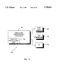
- FIG. 1 is a block diagram illustrating a prior art apparatus having separate phase-locked loops tracking a single input signal.
- FIG. 2 is a block diagram illustrating the present invention.
- FIG. 3 is a partial schematic diagram showing a portion of the control circuits of the dual VCO phase-locked loop of FIG. 2.
- FIG. 4 is a graph showing open loop frequency versus control voltage relationships for the dual VCO phase-locked loop of FIG. 2.
- FIG. 5 is a partial block diagram showing current sources and sink for control of the second VCO of the dual VCO phase-locked loop of FIG. 2.
- FIG. 6 is a partial schematic diagram of a current source which compensates for variations in temperature and voltage.
- FIG. 7 is a graph illustrating the effect of the circuit shown in FIG. 6 for variations in power supply voltage.
- FIG. 8 is a graph illustrating the effect of the circuit shown in FIG. 6 for variations in ambient temperature.
- FIG. 9 is a partial schematic diagram of a current source which compensates for variations in manufacturing process variations.
- FIG. 10 is a graph illustrating the effect of the circuit shown in FIG. 9 for variations in the manufacturing process variations.
- FIG. 11 is a block diagram illustrating the use of the dual VCO phase-locked loop in a single-chip video/graphics processor.
- the dual VCO phase-locked loop 50 (referred to hereafter alternatively as the “dual oscillator loop 50" and the “loop 50") includes a line 52 for receiving a reference input signal f i , a phase-frequency detector 54, a charge pump 56, a loop filter 58, providing a loop control voltage V CNT on line 60, a first VCO 62 including a frequency control circuit 76 and an oscillator 78, the first oscillator providing an output clock signal f o on line 66, a second VCO 64 including an auxiliary frequency control circuit 80 and a second oscillator 82 providing a second output clock signal f c on line 68, and a divider circuit 72.
- a signal and a line carrying the signal will alternatively be referred to by the same identifying numeral.
- the loop control voltage signal V CNT 60 and the line 60 carrying the signal V CNT will be used as appropriate.
- a distinction between the signal and the line carrying the signal will be made when necessary for clarity.
- the phase-frequency detector 54 of the loop 50 compares the reference input signal f i 52 with the output 74 of the divider circuit 72 and uses the result of the comparison to control the loop charge pump 56.
- the charge pump 56 provides an output signal which is passed through the loop filter 58 to provide the loop control voltage V CNT 60.
- the control voltage 60 controls the phase and frequency of the first voltage-controlled oscillator 62.
- the oscillator 62 provides a clock output signal f o 66 which is divided by the divider circuit 72 and fed back to the phase-frequency detector 54 for locking the phase of the output signal f o 66 to the phase of the reference signal f i 52.
- the frequency control circuit 76 supplies an output signal 70 to the second voltage-controlled oscillator 64.
- the signal 70 is received by the auxiliary frequency control circuit 80 and is used to control the frequency of the second oscillator 82.
- FIG. 3 is a partial schematic diagram.
- a portion of the frequency control circuit 76 of FIG. 2 is shown enclosed by a broken line at the left side of FIG. 3, while a portion of the auxiliary frequency control circuit 80 of FIG. 2 is shown enclosed by a broken line at the right side of FIG. 3.
- the line 70 is shown connecting the circuit 76 and the circuit 80.
- the frequency control circuit 76 includes a P-type CMOS transistor 90, an N-type CMOS transistor 92, and a resistor 94.
- the auxiliary frequency control circuit 80 includes a P-type CMOS transistor 96 and a current source 98 which represents an offset current I OFF .
- the line 70 connects the gates of the transistors 90 and 96 which operate as a current mirror.
- the loop control voltage V CNT 60 controls a current I flowing through the transistor 90, and therefore through the connection 70 the loop control voltage V CNT 60 controls a corresponding current ⁇ I flowing through the transistor 96.
- the currents ⁇ I and I OFF control the frequency of the second oscillator 82 (FIG. 2).
- the frequency of the first oscillator 78 is a function of a current I flowing through the transistor 90.
- the frequency of the first oscillator 78 is thus expressed as f(I), and the accuracy of f(I) is controlled by the phase-locked loop 50.
- the frequency of the second oscillator 82 is proportional to the square-root of the sum of the two currents ⁇ I and I OFF . When I OFF ⁇ I, the frequency of the second oscillator 82, f( ⁇ I+I OFF ) ⁇ f( ⁇ I)+1/2f(I OFF ).
- f( ⁇ I) is also controlled by the phase-locked loop 50 by the coupling between the transistors 90 and 96 across line 70, while the term 1/2f(I OFF ) is a function of the semiconductor process variation, the power supply variation and the ambient temperature variation.
- I OFF is intentionally made a function of temperature T, power supply voltage V CC and process variations P in such a way that f(I OFF ) is virtually independent of variations in these parameters.
- FIG. 4 is a graph of frequency versus the loop control voltage V CNT .
- the graph illustrates relationships between the loop control voltage V CNT and f(I) 100, f( ⁇ I+I OFF ) 102, f( ⁇ I) 104, and f(I OFF ) 106.
- the frequency response of the first voltage-controlled oscillator 78 is represented by the curve f(I) 100, and is seen to be a linear function of the control voltage V CNT .
- FIG. 4 also illustrates that the open loop behavior is linear and that the separate effects of ⁇ I and I OFF can be linearly combined, as shown in the curve f( ⁇ I+I OFF ) 102, to predict the behavior of the second voltage-controlled oscillator 82.
- the dependency of I OFF on T, V CC and P is intentionally selected to compensate for variations in these parameters with the result that f(I OFF ) remains essentially flat as seen in the curve 106 of FIG. 4.
- FIG. 5 is a block diagram which illustrates the components of the composite current which determines the frequency of the output signal f e 68 of the second oscillator 82.
- the current components include the offset current I OFF (FIG. 3) and ⁇ I 112.
- the offset current component I OFF is composed of two sub-components, the first being a current source I(P) 108, and the second being a current sink I(T, V CC ) 110.
- the sub-component I(P) 108 is intentionally made a function of the manufacturing process variations, and essentially is independent of variations in ambient temperature and power supply voltage.
- the subcomponent I(T, V CC ) 110 is intentionally made a function of ambient temperature variation and power supply variation, and is virtually independent of variations in the manufacturing process.
- FIG. 6 is a partial schematic diagram illustrating a circuit 120 for providing the current source I(P) which is independent of variations in the ambient temperature and the power supply voltage.
- the circuit 120 includes a current mirror having interconnected P-type CMOS transistors 122, 124, a negative-feedback circuit having interconnected N-type CMOS transistors 126, 128 and a resistor 130.
- FIG. 7 is a graph of the current I(P) versus the power supply voltage V DD .
- the current I(P) 132 remains essentially constant as the power supply voltage V DD is varied over a range from approximately 3.0 V to 3.6 V.
- FIG. 8 is a graph of the current I(P) versus the ambient temperature T.
- the current I(P) 134 remains essentially constant as the ambient temperature T is varied over a range from approximately 20° C. to approximately 125° C.
- FIG. 9 is a partial schematic diagram which illustrates a circuit 140 for providing the current I(T, V CC ), which is independent of variations in manufacturing process.
- the circuit 140 includes resistors 142, 144 forming a voltage divider and driving an operational amplifier 146 connected to the gate of an N-type CMOS transistor 148. A feedback signal to the operational amplifier 146 is developed across a resistor 152.
- a P-type CMOS transistor 150 forms one half of a current mirror and is used for coupling the current I(T, V CC ) through a series of current mirrors (not shown) to its location as a current sink at the control input to the second voltage-controlled oscillator 82 of FIG. 5.
- FIG. 10 is a graph of the current I(T, V CC ) versus the manufacturing process variations, designated generally by the letter P.
- the variation affects circuit speed and is characterized in general as "slow to fast".
- the graph illustrates that the current I(T, V CC ) 154 remains essentially constant as P varies over the 5 process corners (typical, fast-fast, slow-slow, slow-fast and fast-slow).
- FIG. 11 a block diagram of a multimedia display system, designated generally by the numeral 160.
- the display system 160 includes a single-chip video/graphics processor 162 including the dual VCO phase-locked loop 164.
- the display system 160 also includes a flat panel (color LCD) display 166, a color CRT monitor 168, and a color TV 170.
- color LCD color LCD
- the flat panel display 166 is either a DSTN color LCD panel or is a TFT color LCD panel.
- the TV 170 is either a standard US NTSC TV or is a European standard PAL TV.
- the display system can display simultaneously in the following configurations: (1) DSTN and CRT; (2) DSTN and NTSC; (3) DSTN and PAL; (4) TFT and CRT; (5) TFT and NTSC; and (6) TFT and PAL. For each of these combinations, the processor 162 needs two different clock signals each compatible with the refresh needs of one of the display combinations listed here.
- the frequency of the two output signals f c 68 and f o 66 can be selected for compatible operation with the active display devices.
Abstract
Description
Claims (10)
Priority Applications (1)
| Application Number | Priority Date | Filing Date | Title |
|---|---|---|---|
| US08/731,242 US5748044A (en) | 1996-10-11 | 1996-10-11 | Dual VCO phase-locked loop |
Applications Claiming Priority (1)
| Application Number | Priority Date | Filing Date | Title |
|---|---|---|---|
| US08/731,242 US5748044A (en) | 1996-10-11 | 1996-10-11 | Dual VCO phase-locked loop |
Publications (1)
| Publication Number | Publication Date |
|---|---|
| US5748044A true US5748044A (en) | 1998-05-05 |
Family
ID=24938699
Family Applications (1)
| Application Number | Title | Priority Date | Filing Date |
|---|---|---|---|
| US08/731,242 Expired - Lifetime US5748044A (en) | 1996-10-11 | 1996-10-11 | Dual VCO phase-locked loop |
Country Status (1)
| Country | Link |
|---|---|
| US (1) | US5748044A (en) |
Cited By (36)
| Publication number | Priority date | Publication date | Assignee | Title |
|---|---|---|---|---|
| US5870001A (en) * | 1996-10-22 | 1999-02-09 | Telefonaktiebolaget L M Ericsson (Publ) | Apparatus, and associated method, for calibrating a device |
| US6014176A (en) * | 1995-06-21 | 2000-01-11 | Sony Corporation | Automatic phase control apparatus for phase locking the chroma burst of analog and digital video data using a numerically controlled oscillator |
| US6150886A (en) * | 1998-10-20 | 2000-11-21 | Mitsubishi Denki Kabushiki Kaisha | Phase locked loop circuit with multiple combinations which each produce a single phase and multiphase clock signals |
| US6281727B1 (en) | 2000-10-05 | 2001-08-28 | Pericom Semiconductor Corp. | Fine-tuning phase-locked loop PLL using variable resistor between dual PLL loops |
| US6292522B1 (en) * | 1997-11-13 | 2001-09-18 | Lsi Logic Corporation | Frequency decoder databank for phase-locked loop |
| DE10047343A1 (en) * | 2000-09-25 | 2002-05-08 | Siemens Ag | resonator |
| US6441667B1 (en) * | 2001-03-29 | 2002-08-27 | International Business Machines Corporation | Multiphase clock generator |
| US6774912B1 (en) | 2000-03-16 | 2004-08-10 | Matrox Graphics Inc. | Multiple display device display controller with video overlay and full screen video outputs |
| US6794949B1 (en) * | 2003-03-28 | 2004-09-21 | Freescale Semiconductor, Inc. | Frequency generating device and method thereof |
| US20050024100A1 (en) * | 2003-07-29 | 2005-02-03 | Matsushita Electric Industrial Co., Ltd. | Current driver and display device |
| US20050046489A1 (en) * | 2003-08-28 | 2005-03-03 | International Business Machines Corporation | Self-adaptive voltage regulator for a phase-locked loop |
| US20050265117A1 (en) * | 2000-08-18 | 2005-12-01 | Rambus Inc. | Apparatus and method for generating clock signals |
| DE19938515B4 (en) * | 1999-08-13 | 2006-03-23 | Infineon Technologies Ag | Synthesizer for a communication device |
| US20060192229A1 (en) * | 2005-02-28 | 2006-08-31 | Semiconductor Energy Laboratory Co., Ltd. | Semiconductor device and electronic apparatus using the same |
| DE102006007094B3 (en) * | 2006-02-15 | 2007-08-16 | Infineon Technologies Ag | Method for synchronizing a clock signal to a reference signal and phase locked loop |
| US20070200635A1 (en) * | 2006-02-17 | 2007-08-30 | David Meltzer | Methods and apparatus for compensating a variable oscillator for process, voltage, and temperature variations using a replica oscillator |
| US7400333B1 (en) | 2000-03-16 | 2008-07-15 | Matrox Graphics Inc. | Video display system with two controllers each able to scale and blend RGB and YUV surfaces |
| US20110095831A1 (en) * | 2009-10-26 | 2011-04-28 | Himax Technologies Limited | Pvt-independent current-controlled oscillator |
| TWI395087B (en) * | 2009-11-02 | 2013-05-01 | Himax Tech Ltd | Pvt-independent current-controlled oscillator |
| US9083356B1 (en) | 2013-03-14 | 2015-07-14 | Gsi Technology, Inc. | Systems and methods of phase-locked loop involving closed-loop, continuous frequency range, auto calibration and/or other features |
| US9124413B2 (en) | 2011-10-26 | 2015-09-01 | Qualcomm Incorporated | Clock and data recovery for NFC transceivers |
| US10284205B2 (en) | 2016-10-21 | 2019-05-07 | Infineon Technologies Ag | Adaptive bandwidth systems and methods |
| US10521229B2 (en) | 2016-12-06 | 2019-12-31 | Gsi Technology, Inc. | Computational memory cell and processing array device using memory cells |
| US10770133B1 (en) | 2016-12-06 | 2020-09-08 | Gsi Technology, Inc. | Read and write data processing circuits and methods associated with computational memory cells that provides write inhibits and read bit line pre-charge inhibits |
| US10777262B1 (en) | 2016-12-06 | 2020-09-15 | Gsi Technology, Inc. | Read data processing circuits and methods associated memory cells |
| US10847213B1 (en) | 2016-12-06 | 2020-11-24 | Gsi Technology, Inc. | Write data processing circuits and methods associated with computational memory cells |
| US10847212B1 (en) | 2016-12-06 | 2020-11-24 | Gsi Technology, Inc. | Read and write data processing circuits and methods associated with computational memory cells using two read multiplexers |
| US10854284B1 (en) | 2016-12-06 | 2020-12-01 | Gsi Technology, Inc. | Computational memory cell and processing array device with ratioless write port |
| US10860320B1 (en) | 2016-12-06 | 2020-12-08 | Gsi Technology, Inc. | Orthogonal data transposition system and method during data transfers to/from a processing array |
| US10877731B1 (en) | 2019-06-18 | 2020-12-29 | Gsi Technology, Inc. | Processing array device that performs one cycle full adder operation and bit line read/write logic features |
| US10891076B1 (en) | 2016-12-06 | 2021-01-12 | Gsi Technology, Inc. | Results processing circuits and methods associated with computational memory cells |
| US10930341B1 (en) | 2019-06-18 | 2021-02-23 | Gsi Technology, Inc. | Processing array device that performs one cycle full adder operation and bit line read/write logic features |
| US10943648B1 (en) | 2016-12-06 | 2021-03-09 | Gsi Technology, Inc. | Ultra low VDD memory cell with ratioless write port |
| US10958272B2 (en) | 2019-06-18 | 2021-03-23 | Gsi Technology, Inc. | Computational memory cell and processing array device using complementary exclusive or memory cells |
| US10998040B2 (en) | 2016-12-06 | 2021-05-04 | Gsi Technology, Inc. | Computational memory cell and processing array device using the memory cells for XOR and XNOR computations |
| US11227653B1 (en) | 2016-12-06 | 2022-01-18 | Gsi Technology, Inc. | Storage array circuits and methods for computational memory cells |
Citations (2)
| Publication number | Priority date | Publication date | Assignee | Title |
|---|---|---|---|---|
| US4567448A (en) * | 1982-08-05 | 1986-01-28 | Epson Corporation | Variable frequency oscillator |
| US4904955A (en) * | 1987-09-11 | 1990-02-27 | Siemens Aktiengesellschaft | Circuit for generating two closely adjacent frequencies |
-
1996
- 1996-10-11 US US08/731,242 patent/US5748044A/en not_active Expired - Lifetime
Patent Citations (2)
| Publication number | Priority date | Publication date | Assignee | Title |
|---|---|---|---|---|
| US4567448A (en) * | 1982-08-05 | 1986-01-28 | Epson Corporation | Variable frequency oscillator |
| US4904955A (en) * | 1987-09-11 | 1990-02-27 | Siemens Aktiengesellschaft | Circuit for generating two closely adjacent frequencies |
Non-Patent Citations (2)
| Title |
|---|
| Product Data Book, 86CM65 Aurora64V Dual Display Accelerator, Section 11: Flat Panel Interface, S3 Incorporated, Santa Clara, California (Jul. 1996) pp. 1 14. * |
| Product Data Book, 86CM65 Aurora64V+ Dual Display Accelerator, Section 11: Flat Panel Interface, S3 Incorporated, Santa Clara, California (Jul. 1996) pp. 1-14. |
Cited By (63)
| Publication number | Priority date | Publication date | Assignee | Title |
|---|---|---|---|---|
| US6014176A (en) * | 1995-06-21 | 2000-01-11 | Sony Corporation | Automatic phase control apparatus for phase locking the chroma burst of analog and digital video data using a numerically controlled oscillator |
| US5870001A (en) * | 1996-10-22 | 1999-02-09 | Telefonaktiebolaget L M Ericsson (Publ) | Apparatus, and associated method, for calibrating a device |
| US6292522B1 (en) * | 1997-11-13 | 2001-09-18 | Lsi Logic Corporation | Frequency decoder databank for phase-locked loop |
| US6150886A (en) * | 1998-10-20 | 2000-11-21 | Mitsubishi Denki Kabushiki Kaisha | Phase locked loop circuit with multiple combinations which each produce a single phase and multiphase clock signals |
| DE19938515B4 (en) * | 1999-08-13 | 2006-03-23 | Infineon Technologies Ag | Synthesizer for a communication device |
| US6774912B1 (en) | 2000-03-16 | 2004-08-10 | Matrox Graphics Inc. | Multiple display device display controller with video overlay and full screen video outputs |
| US7400333B1 (en) | 2000-03-16 | 2008-07-15 | Matrox Graphics Inc. | Video display system with two controllers each able to scale and blend RGB and YUV surfaces |
| US20050265117A1 (en) * | 2000-08-18 | 2005-12-01 | Rambus Inc. | Apparatus and method for generating clock signals |
| DE10047343B4 (en) * | 2000-09-25 | 2004-04-15 | Siemens Ag | resonator |
| US20040033794A1 (en) * | 2000-09-25 | 2004-02-19 | Christian Korden | Resonator configuration |
| DE10047343A1 (en) * | 2000-09-25 | 2002-05-08 | Siemens Ag | resonator |
| US7065331B2 (en) | 2000-09-25 | 2006-06-20 | Siemens Aktiengesellschaft | Resonator configuration |
| US6281727B1 (en) | 2000-10-05 | 2001-08-28 | Pericom Semiconductor Corp. | Fine-tuning phase-locked loop PLL using variable resistor between dual PLL loops |
| US6480049B2 (en) * | 2001-03-29 | 2002-11-12 | International Business Machines Corporation | Multiphase clock generator |
| US6441667B1 (en) * | 2001-03-29 | 2002-08-27 | International Business Machines Corporation | Multiphase clock generator |
| US6794949B1 (en) * | 2003-03-28 | 2004-09-21 | Freescale Semiconductor, Inc. | Frequency generating device and method thereof |
| US20050024100A1 (en) * | 2003-07-29 | 2005-02-03 | Matsushita Electric Industrial Co., Ltd. | Current driver and display device |
| US20060181491A1 (en) * | 2003-07-29 | 2006-08-17 | Matsushita Electric Industrial Co., Ltd. | Display device comprising display driver having display driving section formed between transistors providing electric current thereto |
| US7145379B2 (en) | 2003-07-29 | 2006-12-05 | Matsushita Electric Industrial Co., Ltd. | Current driver and display device |
| US7649528B2 (en) | 2003-07-29 | 2010-01-19 | Panasonic Corporation | Display device comprising display driver having display driving section formed between transistors providing electric current thereto |
| US6977558B2 (en) | 2003-08-28 | 2005-12-20 | International Busines Machines Corporation | Self-adaptive voltage regulator for a phase-locked loop |
| US20050046489A1 (en) * | 2003-08-28 | 2005-03-03 | International Business Machines Corporation | Self-adaptive voltage regulator for a phase-locked loop |
| US8106594B2 (en) | 2005-02-28 | 2012-01-31 | Semiconductor Energy Laboratory Co., Ltd. | Semiconductor device and electronic apparatus using the same |
| US20060192229A1 (en) * | 2005-02-28 | 2006-08-31 | Semiconductor Energy Laboratory Co., Ltd. | Semiconductor device and electronic apparatus using the same |
| US8946710B2 (en) | 2005-02-28 | 2015-02-03 | Semiconductor Energy Laboratory Co., Ltd. | Semiconductor device and electronic apparatus using the same |
| US20070194819A1 (en) * | 2006-02-15 | 2007-08-23 | Infineon Technologies Ag | Method for synchronizing a clock signal with a reference signal, and phase locked loop |
| US7642821B2 (en) | 2006-02-15 | 2010-01-05 | Infineon Technologies Ag | Method for synchronizing a clock signal with a reference signal, and phase locked loop |
| DE102006007094B3 (en) * | 2006-02-15 | 2007-08-16 | Infineon Technologies Ag | Method for synchronizing a clock signal to a reference signal and phase locked loop |
| US7355482B2 (en) | 2006-02-17 | 2008-04-08 | Seiko Epson Corporation | Methods and apparatus for compensating a variable oscillator for process, voltage, and temperature variations using a replica oscillator |
| US20070200635A1 (en) * | 2006-02-17 | 2007-08-30 | David Meltzer | Methods and apparatus for compensating a variable oscillator for process, voltage, and temperature variations using a replica oscillator |
| US8089326B2 (en) * | 2009-10-26 | 2012-01-03 | Himax Technologies Limited | PVT-independent current-controlled oscillator |
| US20110095831A1 (en) * | 2009-10-26 | 2011-04-28 | Himax Technologies Limited | Pvt-independent current-controlled oscillator |
| TWI395087B (en) * | 2009-11-02 | 2013-05-01 | Himax Tech Ltd | Pvt-independent current-controlled oscillator |
| US9124413B2 (en) | 2011-10-26 | 2015-09-01 | Qualcomm Incorporated | Clock and data recovery for NFC transceivers |
| US9083356B1 (en) | 2013-03-14 | 2015-07-14 | Gsi Technology, Inc. | Systems and methods of phase-locked loop involving closed-loop, continuous frequency range, auto calibration and/or other features |
| US9608651B1 (en) | 2013-03-14 | 2017-03-28 | Gsi Technology, Inc. | Systems and methods of phase-locked loop involving closed-loop, continuous frequency range, auto calibration and/or other features |
| US9722618B1 (en) | 2013-03-14 | 2017-08-01 | Gsi Technology, Inc. | Systems and methods of phase-locked loop involving closed-loop, continuous frequency range, auto calibration and/or other features |
| US9729159B1 (en) | 2013-03-14 | 2017-08-08 | Gsi Technology, Inc. | Systems and methods of phase-locked loop involving closed-loop, continuous frequency range, auto calibration and/or other features |
| US10284205B2 (en) | 2016-10-21 | 2019-05-07 | Infineon Technologies Ag | Adaptive bandwidth systems and methods |
| US10860320B1 (en) | 2016-12-06 | 2020-12-08 | Gsi Technology, Inc. | Orthogonal data transposition system and method during data transfers to/from a processing array |
| US11150903B2 (en) | 2016-12-06 | 2021-10-19 | Gsi Technology, Inc. | Computational memory cell and processing array device using memory cells |
| US10770133B1 (en) | 2016-12-06 | 2020-09-08 | Gsi Technology, Inc. | Read and write data processing circuits and methods associated with computational memory cells that provides write inhibits and read bit line pre-charge inhibits |
| US10777262B1 (en) | 2016-12-06 | 2020-09-15 | Gsi Technology, Inc. | Read data processing circuits and methods associated memory cells |
| US10847213B1 (en) | 2016-12-06 | 2020-11-24 | Gsi Technology, Inc. | Write data processing circuits and methods associated with computational memory cells |
| US10847212B1 (en) | 2016-12-06 | 2020-11-24 | Gsi Technology, Inc. | Read and write data processing circuits and methods associated with computational memory cells using two read multiplexers |
| US10854284B1 (en) | 2016-12-06 | 2020-12-01 | Gsi Technology, Inc. | Computational memory cell and processing array device with ratioless write port |
| US10860318B2 (en) | 2016-12-06 | 2020-12-08 | Gsi Technology, Inc. | Computational memory cell and processing array device using memory cells |
| US10521229B2 (en) | 2016-12-06 | 2019-12-31 | Gsi Technology, Inc. | Computational memory cell and processing array device using memory cells |
| US11763881B2 (en) | 2016-12-06 | 2023-09-19 | Gsi Technology, Inc. | Computational memory cell and processing array device using the memory cells for XOR and XNOR computations |
| US10891076B1 (en) | 2016-12-06 | 2021-01-12 | Gsi Technology, Inc. | Results processing circuits and methods associated with computational memory cells |
| US11409528B2 (en) | 2016-12-06 | 2022-08-09 | Gsi Technology, Inc. | Orthogonal data transposition system and method during data transfers to/from a processing array |
| US10943648B1 (en) | 2016-12-06 | 2021-03-09 | Gsi Technology, Inc. | Ultra low VDD memory cell with ratioless write port |
| US11257540B2 (en) | 2016-12-06 | 2022-02-22 | Gsi Technology, Inc. | Write data processing methods associated with computational memory cells |
| US10998040B2 (en) | 2016-12-06 | 2021-05-04 | Gsi Technology, Inc. | Computational memory cell and processing array device using the memory cells for XOR and XNOR computations |
| US11094374B1 (en) | 2016-12-06 | 2021-08-17 | Gsi Technology, Inc. | Write data processing circuits and methods associated with computational memory cells |
| US10725777B2 (en) | 2016-12-06 | 2020-07-28 | Gsi Technology, Inc. | Computational memory cell and processing array device using memory cells |
| US11227653B1 (en) | 2016-12-06 | 2022-01-18 | Gsi Technology, Inc. | Storage array circuits and methods for computational memory cells |
| US11194519B2 (en) | 2016-12-06 | 2021-12-07 | Gsi Technology, Inc. | Results processing circuits and methods associated with computational memory cells |
| US11205476B1 (en) | 2016-12-06 | 2021-12-21 | Gsi Technology, Inc. | Read data processing circuits and methods associated with computational memory cells |
| US11194548B2 (en) | 2019-06-18 | 2021-12-07 | Gsi Technology, Inc. | Processing array device that performs one cycle full adder operation and bit line read/write logic features |
| US10958272B2 (en) | 2019-06-18 | 2021-03-23 | Gsi Technology, Inc. | Computational memory cell and processing array device using complementary exclusive or memory cells |
| US10930341B1 (en) | 2019-06-18 | 2021-02-23 | Gsi Technology, Inc. | Processing array device that performs one cycle full adder operation and bit line read/write logic features |
| US10877731B1 (en) | 2019-06-18 | 2020-12-29 | Gsi Technology, Inc. | Processing array device that performs one cycle full adder operation and bit line read/write logic features |
Similar Documents
| Publication | Publication Date | Title |
|---|---|---|
| US5748044A (en) | Dual VCO phase-locked loop | |
| US7616075B2 (en) | Phase locked loop circuit having regulator | |
| US7365581B2 (en) | Regulated adaptive-bandwidth PLL/DLL using self-biasing current from a VCO/VCDL | |
| US5414390A (en) | Center frequency controlled phase locked loop system | |
| US6531913B1 (en) | Low voltage charge pump | |
| US6781425B2 (en) | Current-steering charge pump circuit and method of switching | |
| US5629650A (en) | Self-biased phase-locked loop | |
| US4494080A (en) | Voltage-controlled oscillator with independent gain and frequency controls | |
| US6107889A (en) | Phase locked loop charge pump circuit | |
| US7154352B2 (en) | Clock generator and related biasing circuit | |
| US5463352A (en) | Supply voltage tolerant phase-locked loop circuit | |
| US5760657A (en) | Method and apparatus employing a process dependent impedance that compensates for manufacturing variations in a voltage controlled oscillator | |
| JPH06112815A (en) | Charging pump in phase-locked loop | |
| US5081429A (en) | Voltage controlled oscillator with controlled load | |
| JPH06216767A (en) | Phase locked loop circuit having stabilized phase discriminator | |
| US5479073A (en) | Dot clock generator for liquid crystal display device | |
| EP0545517A1 (en) | Gate multiplexed low noise charge pump | |
| US20020000886A1 (en) | Voltage controlled oscillator | |
| US6430244B1 (en) | Digital phase-locked loop apparatus with enhanced phase error compensating circuit | |
| US6188739B1 (en) | Modified third order phase-locked loop | |
| US6985045B2 (en) | Gain control circuits for voltage controlled oscillators | |
| JP2766103B2 (en) | Phase locked loop | |
| JPH10200382A (en) | Voltage controlled oscillator circuit for low voltage driving | |
| US6563354B1 (en) | On-chip circuit to compensate output drive strength across process corners | |
| KR20140124589A (en) | Charge pump and phase locked loop circuit |
Legal Events
| Date | Code | Title | Description |
|---|---|---|---|
| AS | Assignment |
Owner name: SILICON MOTION, INC., CALIFORNIA Free format text: ASSIGNMENT OF ASSIGNORS INTEREST;ASSIGNOR:XUE, YUAN;REEL/FRAME:008218/0284 Effective date: 19961011 |
|
| AS | Assignment |
Owner name: IMPERIAL BANK, CALIFORNIA Free format text: SECURITY AGREEMENT;ASSIGNOR:SILICON MOTION, INC.;REEL/FRAME:009472/0477 Effective date: 19980915 |
|
| AS | Assignment |
Owner name: VENTURE BANKING GROUP., A DIVISION OF CUPERTINO NA Free format text: SECURITY INTEREST;ASSIGNOR:SILICON MOTION, INC.;REEL/FRAME:010154/0107 Effective date: 19990803 |
|
| STCF | Information on status: patent grant |
Free format text: PATENTED CASE |
|
| CC | Certificate of correction | ||
| AS | Assignment |
Owner name: VENTURE BANKING GROUP, A DIVISION OF CUPERTINO NAT Free format text: SECURITY INTEREST;ASSIGNOR:SILICON MOTION, INC.;REEL/FRAME:011064/0674 Effective date: 20000727 |
|
| FEPP | Fee payment procedure |
Free format text: PAYOR NUMBER ASSIGNED (ORIGINAL EVENT CODE: ASPN); ENTITY STATUS OF PATENT OWNER: LARGE ENTITY |
|
| AS | Assignment |
Owner name: SILICON MOTION, INC., CALIFORNIA Free format text: REASSIGNMENT AND RELEASE OF SECURITY INTEREST;ASSIGNOR:IMPERIAL BANK;REEL/FRAME:012025/0978 Effective date: 20000817 |
|
| REMI | Maintenance fee reminder mailed | ||
| FEPP | Fee payment procedure |
Free format text: PAT HOLDER NO LONGER CLAIMS SMALL ENTITY STATUS, ENTITY STATUS SET TO UNDISCOUNTED (ORIGINAL EVENT CODE: STOL); ENTITY STATUS OF PATENT OWNER: LARGE ENTITY |
|
| REFU | Refund |
Free format text: REFUND - PAYMENT OF MAINTENANCE FEE, 4TH YR, SMALL ENTITY (ORIGINAL EVENT CODE: R283); ENTITY STATUS OF PATENT OWNER: LARGE ENTITY |
|
| FPAY | Fee payment |
Year of fee payment: 4 |
|
| SULP | Surcharge for late payment | ||
| FPAY | Fee payment |
Year of fee payment: 8 |
|
| FPAY | Fee payment |
Year of fee payment: 12 |