US5751525A - EOS/ESD Protection circuit for an integrated circuit with operating/test voltages exceeding power supply rail voltages - Google Patents
EOS/ESD Protection circuit for an integrated circuit with operating/test voltages exceeding power supply rail voltages Download PDFInfo
- Publication number
- US5751525A US5751525A US08/583,612 US58361296A US5751525A US 5751525 A US5751525 A US 5751525A US 58361296 A US58361296 A US 58361296A US 5751525 A US5751525 A US 5751525A
- Authority
- US
- United States
- Prior art keywords
- breakdown
- circuit
- voltage
- clamping
- mode
- Prior art date
- Legal status (The legal status is an assumption and is not a legal conclusion. Google has not performed a legal analysis and makes no representation as to the accuracy of the status listed.)
- Expired - Lifetime
Links
- 238000012360 testing method Methods 0.000 title description 33
- 230000015556 catabolic process Effects 0.000 claims description 162
- 230000000694 effects Effects 0.000 claims description 8
- 239000000758 substrate Substances 0.000 claims description 8
- 239000004065 semiconductor Substances 0.000 claims description 6
- 239000004020 conductor Substances 0.000 claims description 4
- 238000009792 diffusion process Methods 0.000 description 7
- 238000010586 diagram Methods 0.000 description 6
- 238000004519 manufacturing process Methods 0.000 description 6
- 230000001052 transient effect Effects 0.000 description 6
- 238000013459 approach Methods 0.000 description 3
- 238000013461 design Methods 0.000 description 3
- 238000007599 discharging Methods 0.000 description 3
- 239000002184 metal Substances 0.000 description 3
- 238000000034 method Methods 0.000 description 3
- 238000010998 test method Methods 0.000 description 3
- XUIMIQQOPSSXEZ-UHFFFAOYSA-N Silicon Chemical compound [Si] XUIMIQQOPSSXEZ-UHFFFAOYSA-N 0.000 description 2
- 230000004075 alteration Effects 0.000 description 2
- 230000008901 benefit Effects 0.000 description 2
- 230000006872 improvement Effects 0.000 description 2
- 238000012986 modification Methods 0.000 description 2
- 230000004048 modification Effects 0.000 description 2
- 229910021420 polycrystalline silicon Inorganic materials 0.000 description 2
- 229920005591 polysilicon Polymers 0.000 description 2
- 230000008569 process Effects 0.000 description 2
- 230000009467 reduction Effects 0.000 description 2
- 229910052710 silicon Inorganic materials 0.000 description 2
- 239000010703 silicon Substances 0.000 description 2
- 230000008859 change Effects 0.000 description 1
- 238000005229 chemical vapour deposition Methods 0.000 description 1
- 238000010276 construction Methods 0.000 description 1
- 230000007613 environmental effect Effects 0.000 description 1
- 238000010438 heat treatment Methods 0.000 description 1
- 238000005468 ion implantation Methods 0.000 description 1
- 229910044991 metal oxide Inorganic materials 0.000 description 1
- 150000004706 metal oxides Chemical class 0.000 description 1
- 238000001465 metallisation Methods 0.000 description 1
- 230000035945 sensitivity Effects 0.000 description 1
Images


Classifications
-
- G—PHYSICS
- G01—MEASURING; TESTING
- G01R—MEASURING ELECTRIC VARIABLES; MEASURING MAGNETIC VARIABLES
- G01R31/00—Arrangements for testing electric properties; Arrangements for locating electric faults; Arrangements for electrical testing characterised by what is being tested not provided for elsewhere
- G01R31/001—Measuring interference from external sources to, or emission from, the device under test, e.g. EMC, EMI, EMP or ESD testing
- G01R31/002—Measuring interference from external sources to, or emission from, the device under test, e.g. EMC, EMI, EMP or ESD testing where the device under test is an electronic circuit
-
- H—ELECTRICITY
- H01—ELECTRIC ELEMENTS
- H01L—SEMICONDUCTOR DEVICES NOT COVERED BY CLASS H10
- H01L27/00—Devices consisting of a plurality of semiconductor or other solid-state components formed in or on a common substrate
- H01L27/02—Devices consisting of a plurality of semiconductor or other solid-state components formed in or on a common substrate including semiconductor components specially adapted for rectifying, oscillating, amplifying or switching and having at least one potential-jump barrier or surface barrier; including integrated passive circuit elements with at least one potential-jump barrier or surface barrier
- H01L27/0203—Particular design considerations for integrated circuits
- H01L27/0248—Particular design considerations for integrated circuits for electrical or thermal protection, e.g. electrostatic discharge [ESD] protection
- H01L27/0251—Particular design considerations for integrated circuits for electrical or thermal protection, e.g. electrostatic discharge [ESD] protection for MOS devices
-
- H—ELECTRICITY
- H01—ELECTRIC ELEMENTS
- H01L—SEMICONDUCTOR DEVICES NOT COVERED BY CLASS H10
- H01L29/00—Semiconductor devices adapted for rectifying, amplifying, oscillating or switching, or capacitors or resistors with at least one potential-jump barrier or surface barrier, e.g. PN junction depletion layer or carrier concentration layer; Details of semiconductor bodies or of electrodes thereof ; Multistep manufacturing processes therefor
- H01L29/66—Types of semiconductor device ; Multistep manufacturing processes therefor
- H01L29/68—Types of semiconductor device ; Multistep manufacturing processes therefor controllable by only the electric current supplied, or only the electric potential applied, to an electrode which does not carry the current to be rectified, amplified or switched
- H01L29/70—Bipolar devices
- H01L29/72—Transistor-type devices, i.e. able to continuously respond to applied control signals
- H01L29/73—Bipolar junction transistors
- H01L29/732—Vertical transistors
- H01L29/7322—Vertical transistors having emitter-base and base-collector junctions leaving at the same surface of the body, e.g. planar transistor
Definitions
- the present invention relates generally to integrated circuits, and more particularly, to a method and apparatus for protecting integrated circuits from electrical overstress (EOS) and in particular from electrostatic discharge (ESD).
- EOS electrical overstress
- ESD electrostatic discharge
- EOS Electrical overstress
- ESD electrostatic discharge
- Electrostatic discharge is a well-known cause of failure for integrated circuits.
- the buildup of electrostatic charge on personnel and equipment during the manufacture and use of integrated circuits may assume potentials as high as 30,000 volts with respect to an ESD reference point.
- the buildup charge may be discharged through an integrated circuit when either the personnel or the equipment comes in contact with or in close proximity to the integrated circuit.
- the electrostatic discharge may occur during manufacturing or testing when the integrated circuit is non-operating, or may occur when the integrated circuit is installed in a device and is operating.
- Integrated circuits are particularly susceptible to ESD damage during handling in a manufacturing or testing environment.
- test procedures exist for testing integrated circuits and determining sensitivity threshold levels of integrated circuits to electrostatic discharge. These test procedures include: American National Standards Institute (ANSI)/ESD Association Standard S5.1 Human Body Model (HBM) for simulating an ESD event generated by the human body; ANSI/ESD Association Standard S5.2 Machine Model (MM) for simulating an ESD event generated by a charged metal object such as a machine; and ANSI/ESD Association Draft Standard DS5.3 Socketed Charge Device Model (SCDM) for simulating electrostatic discharges to integrated circuits during manufacture and test due to the use of automated equipment. Because of the pervasive use of automated equipment in testing, handling and manufacturing of integrated circuits, SCDM discharges are the predominant cause of manufacturing-related ESD failures.
- ANSI/ESD Association Standard S5.1 Human Body Model (HBM) for simulating an ESD event generated by the human body
- MM Machine Model
- SCDM Socketed Charge Device Model
- MOS transistors are particularly sensitive to electrostatic discharge to input and output pins.
- ESD protection circuits have been developed to protect MOS transistors from ESD events at their input and output pins. These approaches typically rely on diodes, diode-connected bipolar devices having their emitter shorted to their base, or diode-connected MOS devices having their gate directly or resistively connected to their source. These devices are typically used between each Input/Output (I/O) pad of the integrated circuit and one or more voltage reference pads.
- I/O Input/Output
- PNP punch-through devices have been used to provide EOS/ESD protection and allow voltages at I/O pins to significantly exceed the supply voltage. There are however several disadvantages to using punch-through devices. Punch-through devices typically provide less than two kilovolt ESD protection when tested in accordance with the human body model, and the punch-through threshold voltage of these devices is not sufficiently controllable to provide adequate protection to small geometry CMOS transistors.
- diode-connected transistors have also been used to provide EOS/ESD protection in integrated circuit applications that require a voltage at an I/O pad in excess of a supply voltage. These schemes typically have high turn-on voltages, typically on the order of 35 to 65 volts, making them unsuitable for protecting small geometry (CMOS) transistors. Further, back-to-back, diode-connected transistors are susceptible to latch-up conditions, particularly when used on bipolar-CMOS or CMOS processes, and may act like a silicon controlled rectifier (SCR), staying on with a low holding voltage (approximately 2 volts) even after the overvoltage condition has passed.
- SCR silicon controlled rectifier
- SCR Silicon controlled rectifiers
- diode-connected transistors discussed above, SCRs are also susceptible to latch-up problems. Further, the trigger voltage of an SCR is difficult to monitor and control since SCRs are typically based on non-standard devices.
- An object of the present invention is to provide an EOS/ESD protection scheme that can be used on I/O pins having operational voltages that exceed a supply voltage of the integrated circuit and that overcome the limitations of devices used in the prior art.
- an EOS/ESD protection circuit for protecting an active circuit from electrical overstress.
- the EOS/ESD protection circuit includes first and second clamping circuits connected between a first input and a first signal pad of the electrical overstress protection circuit.
- the first clamping circuit includes a breakdown device that conducts current in a first direction when a voltage across the breakdown device exceeds a forward conduction threshold.
- the second clamping circuit includes a breakdown device that in a first direction of current through the breakdown device has an active mode of operation and a breakdown mode of operation. The breakdown mode of operation occurs when a voltage across the breakdown device exceeds a reverse breakdown threshold.
- the breakdown device switches from the breakdown mode to the active mode when a magnitude of a current through the breakdown device in the first direction exceeds a current threshold level.
- the electrical overstress protection circuit further includes third and fourth clamping circuits series connected between a first output and a second signal pad of the protection circuit.
- each of the breakdown devices of the first and second clamping circuits is a bipolar transistor having a base with a resistance such that when a magnitude of a current through the base region in breakdown mode exceeds a threshold level a voltage is created across the base and switches the bipolar transistor from the breakdown mode to the active mode.
- the third and fourth clamping circuits comprise MOS transistors.
- the third and fourth clamping circuits of the previously described embodiment have a combined breakdown voltage and a first discharge current path is formed from the first input to the first signal pad of the EOS/ESD protection circuit through the third and fourth clamping circuits when a voltage from the first input to the first signal pad exceeds the combined breakdown voltage.
- the magnitude of the combined breakdown voltage of the third and fourth clamping circuits is less than the magnitude of the sum of the forward conduction threshold of the first clamping circuit and the reverse breakdown threshold of the second clamping circuit.
- an electrical overstress protection circuit for protecting an active circuit from EOS/ESD events includes first and second inputs for receiving first and second reference voltages of the active circuit, first and second outputs for providing the first and second reference voltages to the active circuit, and first and second signal pads for respectively connecting to an external circuit and the active circuit.
- the protection circuit in accordance with this embodiment further includes first means for protecting the active circuit from an electrical overstress voltage at the first input having one of a positive or negative polarity with respect to the first signal pad.
- the first means for protecting has an off mode in which the first means for protecting has substantially no effect on the operation of the active circuit, and an on mode in which the first means for protecting limits an absolute value of a voltage at the first output with respect to the second signal pad to less than a predetermined clamping voltage value.
- the first means for protecting includes switching means for switching from the off mode to the on mode when an absolute voltage value of an electrical overstress voltage at the first input with respect to the first signal pad exceeds a first threshold value that is greater than the first reference value by at least approximately two volts.
- the electrical overstress protection circuit further includes second means for protecting the active circuit from an electrical overstress voltage at the second input having one of a positive or negative polarity with respect to the first signal pad.
- the second means for protecting has an off mode in which the second means for protecting has substantially no effect on the operation of the active circuit, and an on mode in which the second means for protecting limits an absolute value of a voltage at the second output with respect to the second signal pad to less than the predetermined clamping voltage value.
- the second means for protecting including switching means for switching from the off mode to the on mode when an absolute value of an electrical overstress voltage at the second input with respect to the first signal pad exceeds a second threshold value that is less than the second reference value by at least approximately two volts.
- FIG. 1 is a schematic diagram of an integrated circuit including an EOS/ESD protection circuit
- FIG. 2 is a schematic diagram of an integrated circuit including an EOS/ESD protection circuit in accordance with a first embodiment of the present invention
- FIG. 3 is a plan view of an EOS/ESD protection circuit in accordance with one embodiment of the present invention.
- FIG. 4 is a cross-sectional view of FIG. 3 taken along line A--A of FIG. 3;
- FIG. 5 is a schematic diagram of a first equivalent circuit of the first embodiment of the present invention.
- FIG. 6 is a schematic diagram of a second equivalent circuit of the first embodiment of the present invention.
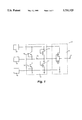
- FIG. 7 is a schematic diagram of an EOS/ESD protection circuit in accordance with a second embodiment of the present invention.
- FIG. 8 is a schematic diagram of an EOS/ESD protection circuit in accordance with a third embodiment of the present invention.
- FIG. 1 shows a protection scheme disclosed in co-pending U.S. patent application Ser. No. 08/123,604, assigned to the assignee of this application and incorporated herein by reference.
- an integrated circuit 10 includes an active circuit 14 including one or more transistors, and an ESD protection circuit 12 for protecting the transistors of the active circuit 14.
- the ESD protection circuit 12 includes two breakdown transistors 15 and 16 respectively coupled between an I/O pad 24 and first and second input reference voltage pads 18 and 19.
- the first and second input reference voltage pads 18 and 19 are for receiving a supply voltage and a reference voltage (i.e., ground).
- the ESD protection circuit 12 further includes two PMOS transistors 26 and 28 and a resistor 22. As described further in U.S. patent application Ser. No.
- each of transistors 15, 16, 26, and 28 operates as a diode having a reverse breakdown mode in which the transistor conducts current to protect the active circuit 14 from EOS/ESD events. For example, when an EOS/ESD event occurs at pad 24 having a positive voltage with respect to pad 19, and a breakdown threshold of transistor 16 is exceeded, transistor 16 conducts current from pad 24 to pad 19 to prevent harmful voltages from damaging the active circuit 14.
- Transistors 15 and 16 in addition to operating in the reverse breakdown mode, may also operate as a diode in a forward conduction mode when a voltage at the common emitter and base exceeds a voltage at the collector by a value greater than a diode voltage drop.
- This forward conduction voltage is typically approximately 0.6 volts. Therefore, the DC operating voltage at the I/O pad 24 has a specified maximum DC rating of less than approximately 0.6 volts (and typically less than 0.3 volts to provide a safety margin) beyond the supply voltage at the first voltage reference pad 18. If the voltage at the I/O pad exceeds the maximum DC rating, transistors 15 and 16 will conduct DC current and may sustain damage if the DC current is not limited.
- FIG. 2 One embodiment of an EOS/ESD protection circuit for protecting internal devices of an integrated circuit 40 from electrical overstress and electrostatic discharge is shown in FIG. 2.
- a voltage at an I/O pin may exceed the supply voltage.
- the integrated circuit 40 includes an EOS/ESD protection circuit 42, an active circuit 44, an I/O pad 46 for connecting to an I/O pin of the integrated circuit 40, a first input reference voltage pad 48 for connecting to a supply voltage, and a second input reference voltage pad 50 for connecting to a ground reference.
- the active circuit 44 is connected to the EOS/ESD protection circuit 42 at a first voltage reference node 124, at a second voltage reference node 128 and at an I/O node 126.
- the active circuit is also coupled to an output 17 of the integrated circuit 40.
- the active circuit is shown as a PMOS transistor 130 and an NMOS transistor 132 connected as an inverter, but this circuit may include any number of components and is not necessarily limited to CMOS transistors.
- the EOS/ESD protection circuit 42 includes four diode-connected, vertical NPN transistors 52, 60, 68 and 76, each having a respective base 56, 64, 72, and 80 connected to a respective emitter 54, 62, 74, and 78.
- Transistor 52 has its emitter 54 connected to the second input reference voltage pad 50 and its collector 58 connected to the first input reference voltage pad 48.
- Transistor 60 has its emitter 62 connected to the first input reference voltage pad 46, and its collector 66 connected to the collector 70 of transistor 68.
- the emitter 74 of transistor 68 is connected to the I/O pad 46.
- the emitter 78 of transistor 76 is connected to the second input reference voltage pad 50, and the collector 82 of transistor 76 is connected to the I/O pad 46.
- the EOS/ESD protection circuit 42 also includes a pair of resistors 83 and 85.
- Resistor 85 is connected between the first input reference voltage pad 48 and the first voltage reference node 124.
- Resistor 83 is connected between the I/O pad 46 and the I/O node 126.
- the resistors 83 and 85 are formed above the substrate of the integrated circuit 40 by the process of chemical vapor deposition and have a resistance of approximately 153 ohms.
- the EOS/ESD protection circuit 42 further includes four diode-connected, enhancement-mode PMOS transistors 84, 94, 104, and 114, each having a respective back gate 92, 102,112, and 122 connected to a respective source 90,100, 106, and 120, and each PMOS transistor also having a respective gate 88, 98, 108, and 118 connected to a respective source 90, 100,106, and 120.
- Drain 86 of PMOS transistor 84 is connected to the second input reference voltage pad 50, and the source 90 of PMOS transistor 84 is connected to the first voltage reference node 124.
- Drain 96 of transistor 94 is connected to the first voltage reference node 124, and the source 100 of transistor 94 is connected to the source 106 of transistor 104.
- Drain 110 of transistor 104 is connected to the I/O node 126.
- the source 120 of transistor 114 is connected to the I/O node 126 and the drain 122 of transistor 114 is connected to the second input reference voltage pad 50
- FIG. 3 shows a plan view of the embodiment of the present invention shown in schematic form in FIG. 2, except that the active circuit 14, diffused layers and dielectric layers are omitted from FIG. 3 for clarity.
- the components shown in FIG. 3 are connected with various metal conductors 140, 142, 144, 146, 148, 150, 152, and 154 to provide the circuit connections shown in FIG. 2.
- Each of the PMOS transistors 84, 94, 104 and 114 of the EOS/ESD protection circuit 42 shown in FIGS. 2 and 3 are substantially identical, with the exception that transistors 94 and 104 are merged (i.e., they share the same back gate (BG)).
- Each of the PMOS transistors has a gate width of eighteen micrometers ( ⁇ m) and a gate length of five ⁇ m, and the spacing between the drain contact and the gate polysilicon is four ⁇ m.
- the PMOS transistors of the ESD protection circuit 42 are standard PMOS devices.
- FIG. 4 shows a cross-sectional side view of transistor 68 taken along line A--A of FIG. 3.
- NPN transistor 68 comprises a semiconductor substrate 160 onto which an epitaxial layer 158 is grown.
- a buried layer 162 is sandwiched between the substrate 160 and the epitaxial layer 158.
- Above the epitaxial layer 158 are two diffusion regions or ion implantation layers that form the base 72 and the emitter 74 of the transistor 68.
- a portion of the base 72 is located directly under the emitter 74.
- the emitter 74 is below a polysilicon layer 73.
- the collector 70 of transistor 68 merges with buried layer 162 through one of two NPLUGs 164.
- a dielectric layer 156 and an oxide layer 168 of the integrated circuit 40 are also shown in FIG. 4 along with metal conductors 140 and 142.
- Each of diode-connected, vertical NPN transistors 52, 60, 68 and 76 is substantially identical, except that transistors 60 and 68 are merged (i.e., they share the same collector as shown in FIG. 3).
- Each of transistors 52, 60, 68 and 76 has a collector-emitter-base layout and has its respective emitter shorted to its base by metalization to provide the diode connection.
- each of the NPN transistors is substantially a standard transistor except that the emitter area is 5 ⁇ m by 20 ⁇ m, the NPLUG to base spacing is greater than or equal to 15 ⁇ m and the spacing between the base and emitter contacts is greater than or equal to 6 ⁇ m.
- FIG. 5 shows an approximately equivalent circuit (as verified by electrical microprobe analysis) of EOS/ESD protection circuit 42 of FIG. 2 during what is defined as the normal mode of operation of integrated circuit 40.
- the supply voltage connected to the first input reference voltage pad 48 is approximately five volts
- the voltage at the ground reference is approximately zero volts
- the voltage at the I/O pad is between zero and five volts.
- each of the PMOS transistors 84, 94, 104, and 114 of the ESD protection circuit 42 has been replaced by a respective reverse-biased diode 184, 188, 190 and 194, each of which is formed by the drain to back gate junction of each of the transistors, in series with a respective resistor 182, 186, 192 and 196 having substantially equal resistance values that are a function of the layout and sheet resistances of the layers of the integrated circuit 40.
- each of transistors 52, 68 and 76 has a respective resistor 178, 172 and 180 between its emitter and its base. These resistors are substantially equivalent and represent the effective base to emitter resistance which is a function of the layout and sheet resistances of the base and emitter diffusions of the transistors.
- Transistor 60 of FIG. 2 has been replaced in FIG. 5 by a forward biased diode 176, which is formed by the base to collector junction of transistor 60, in series with an associated resistor 174.
- the resistance value of resistor 174 is a function of the base and emitter diffusions of transistor 60.
- transistors 52, 68 and 76 will be off as the voltage from the collector to the emitter for each of the transistors is less than the collector to emitter breakdown voltage with the emitter shorted to the base (BV CES ).
- the value of BV CES for each of transistors 52, 60, 68, and 76 is approximately 33 volts.
- Diodes 184, 190 and 194 are also off in the normal mode of operation as they are reversed biased with a voltage less than their reverse breakdown voltage. Each of diodes 176 and 188 is forward biased with a voltage greater than 0.6 volts and therefore is on.
- the EOS/ESD protection circuit 42 does not draw any appreciable current.
- the EOS/ESD protection circuit 42 does introduce a low impedance of approximately 153 ohms in the input path of the active circuit 44.
- the EOS/ESD protection circuit 42 is used to protect CMOS gates having a high input impedance, and the effect of the 153 ohm resistance is negligible. Accordingly, the EOS/ESD protection circuit 42 has negligible effects on the operation of the integrated circuit during the normal mode of operation in the absence of an EOS or ESD event.
- FIG. 6 shows an approximately equivalent circuit (as verified by electrical microprobe analysis) of EOS/ESD protection circuit 42 of FIG. 2 during what is defined as the special mode of operation of integrated circuit 40.
- the voltage of the voltage supply connected to the first input reference pad 48 is approximately five volts
- the voltage at the ground reference is approximately zero volts
- the voltage at the I/O pad 46 is between approximately 5.9 volts and ten volts.
- the equivalent circuit of transistor 60 in FIG. 6 includes the transistor 60 with a resistor 204 between its emitter 62 and its base 64.
- Resistor 204 is substantially equivalent to resistors 178 and 180 and is a function of the base and emitter diffusions of transistor 60.
- Transistor 68 of FIG. 2 is replaced in FIG. 6 by a diode 200 and a resistor 202 which are substantially equivalent to diode 176 and resistor 174 of FIG. 5.
- the operation of the EOS/ESD protection circuit 42 of FIG. 2, as represented by its equivalent circuit of FIG. 6 during the special mode, in the absence of an EOS/ESD event, is similar to the operation during the normal mode described above. The only significant differences being that in the special mode of operation, diodes 190 and 200 are on, and transistor 60 and diode 188 are off. In the special mode of operation, as in the normal mode of operation, the ESD protection circuit has little or no effect on the operation of the integrated circuit 40 in the absence of an EOS or ESD event.
- the operation of the EOS/ESD protection circuit 42 will now be described during EOS/ESD events.
- the first case to be considered is an EOS or ESD event at the I/O pad 46 having a positive polarity with respect to the first input reference voltage pad 48.
- the reverse breakdown voltage of each of diodes 184, 188, 190 and 194 is approximately 18 volts and the forward bias voltage is approximately 0.6 volts. Therefore, when the magnitude of the EOS or ESD transient voltage exceeds 18.6 volts, both diodes 190 and 188 will conduct current completing a discharge path through resistors 85, 192, 186, and 83 and the diodes 188 and 190.
- Diodes 190 and 188 are protected from drawing excessive current (and the possibility of damage) by resistors 83 and 85. As the transient voltage rises, and the current through diodes 188 and 190 increases, the voltage drop across each of resistors 85, 192, 186 and 83 also increases. Once the magnitude of the sum of the voltage drops across the diode pair (approximately 18.6 volts) and the sum of the voltage drops across each of resistors 85, 192, 186 and 83 exceeds approximately 34 volts, current will flow through diode 200 and transistor 60. Under these conditions, diode 200 is forward biased with a voltage of 0.6 volts, and the base to collector junction of transistor 60 will exhibit an avalanche breakdown when the voltage across the junction exceeds approximately 33.4 volts.
- the avalanche current through transistor 60 will initially primarily follow a path from the collector 70 through the base region 72 under the emitter region 74 to the conductor 140 connected to the base.
- the region of the base diffusion layer 72 disposed under the emitter 74 is relatively resistive and the current following path 170 results in a voltage drop across the base diffusion layer 72.
- transistor 60 conducts current primarily in an active mode of operation.
- the spacing between the base contact and the emitter contact is 6 ⁇ m (verses typical applications of 4.5 ⁇ m) triggering the onset of the active mode of conduction at a relatively low current.
- the required current to trigger the active mode has been measured to be approximately 10 milliamps.
- the current path through transistor 60 during active mode is represented in FIG. 4, by arrow 172.
- electrons are emitted by the emitter 74, flow primarily vertically through the base/emitter junction, through the base region 72 to the buried layer 162, to the NPLUG 164 and out the collector 70.
- the direction of the current shown by arrow 172 is opposite that of the electron flow described above.
- One of the primary benefits of the active mode of transistor 60 vs. the breakdown mode is a reduction in current density through the transistor.
- substantially all of the EOS/ESD current passes through the relatively shallow vertical sidewall of the base resulting in a high current density, excessive localized heating, and a high susceptibility to junction damage at relatively low EOS/ESD currents.
- the current path 172 of the EOS/ESD current is vertical through the relatively large (5 ⁇ m by 20 ⁇ m) emitter diffusion area, resulting in much lower current densities in the transistor and therefore a higher robustness to junction damage.
- a second benefit of embodiments of the present invention is a reduction in power dissipation in the transistor 60 due to an abrupt drop in voltage across the transistor at the onset of the active conduction mode.
- the initial breakdown voltage of transistor 60 (approximately 33 volts) drops to approximately 10 volts in the active mode.
- the instantaneous power dissipation of the transistor which is equal to the product of the voltage and current at a given time, is substantially reduced in active mode.
- Diodes 188 and 190 limit the voltage at node 126 relative to node 124 to approximately 18.6 volts (the voltage drops across resistors 186 and 192 are negligible) which is below the breakdown voltage of internal gates or other dielectric layers of typical components of integrated circuits.
- the voltage across resistor 204 drops below 0.6 volts, transistor 60 turns off, and after the transient voltage at I/O pad 46 drops below approximately 18.6 volts relative to the first input reference voltage pad 48, diodes 188 and 190 no longer conduct.
- the EOS/ESD protection circuit 42 then returns to its high impedance, low leakage current, inactive state.
- the operation of the protection circuit during an EOS or ESD event at the first input reference voltage pad 48 having a positive polarity with respect to the I/O pad 46 is substantially the same as the operation during an EOS or ESD event at the I/O pad having a positive voltage with respect to the first input reference voltage pad 48 described above.
- transistor 68 rather than transistor 60 will conduct current in an active mode, transistor 60 will act as a forward biased diode rather than transistor 68, and the voltage at node 126 relative to node 124 will be approximately negative 18.6 volts rather than positive 18.6 volts.
- the EOS/ESD protection circuit 42 protects the components of the active circuit 44 in a similar manner to that described above as follows with reference to FIG. 6.
- Diode 184 will exhibit a reverse breakdown and conduct the EOS/ESD current when the EOS/ESD transient voltage exceeds a level of approximately 18 volts creating an EOS/ESD discharge path through resistor 83, diode 184 and resistor 182.
- transistor 52 When the total voltage drop across resistors 83 and 182 and diode 184 exceeds approximately 33.4 volts, transistor 52 will exhibit breakdown and begin to conduct current. When the current through transistor 52 exceeds approximately 10 milliamps, transistor 52 will enter the active mode of operation and safely dissipate the EOS/ESD current at a relatively low voltage.
- the discharge path of the EOS/ESD protection circuit does not include any avalanching junctions.
- diode-connected transistors 76 and 114 of FIG. 2 will be forward biased and dissipate the EOS/ESD current.
- the EOS/ESD current through transistor 76 will be greater than through transistor 114 as the discharge path through transistor 114 includes the series resistor 83.
- Transistor 76 due to its relatively large size and the low instantaneous power dissipation associated with forward-biased conduction, can effectively dissipate relatively large EOS/ESD currents.
- transistors 52 and 84 will be forward biased and dissipate the EOS/ESD current.
- ESD performance testing was conducted on three samples each of two different integrated circuits (IC1, IC2) incorporating the EOS/ESD protection device of the embodiment of the present invention shown in FIG. 2 on each I/O pin of the integrated circuits.
- the testing was conducted using a KeyTek Model 7/2 Zap/LatchMaster System manufactured by KeyTek Instrument Corp. of Wilmington, Mass. Testing was conducted in accordance with the ANSI/ESD Association Standard S5.1 Human Body Model (HBM), the ANSI/ESD Association Standard S5.2 Machine Model (MM) and the ANSI/ESD Association Draft Standard DS5.3 Socketed Charged Device Model (SCDM).
- HBM Human Body Model
- MM ANSI/ESD Association Standard S5.2 Machine Model
- SCDM Socketed Charged Device Model
- each individual I/O pin of the integrated circuit under test was subjected to an electrostatic discharge stress sequence with respect to each individual supply pin as well as to a group of all other I/O pins of the integrated circuit.
- Each stress sequence consisted of three positive electrostatic discharges and three negative electrostatic discharges.
- the HBM testing was initiated with ESD amplitudes of 250 volts and increased in 250 volt increments, while the MM testing was initiated at an ESD amplitude of 25 volts and increased in 25 volt increments.
- the substrate pins of the integrated circuit (corresponding to the ground pins) were used to charge the samples under test, and discharging was accomplished through each of the I/O pins of the integrated circuit that were protected by the EOS/ESD protection circuit shown in FIG. 2. For each discharging sequence, three positive and three negative ESD pulses were used. The SCDM testing was initiated with an ESD amplitude of 100 volts and was increased in 100 volt increments.
- Failure criteria for the ESD testing was established as follows.
- the input current at each I/O pin of the integrated circuit under test was measured after each sequence of three stresses under two conditions: 1) with the input voltage at the I/O pin at 5.0 volts and with the supply voltage at 5.0 volts, and 2) with the input voltage at the I/O pin at 0.0 volts and the supply voltage at 5.0 volts.
- a failure was identified when the measured current exceeded 10 microamps.
- the input current was measured with an input voltage of 10 volts at each I/O pin to detect any ESD damage that could degrade the performance of the pins when operating in the special mode described previously. Again, a failure was identified when the measured current exceeded 10 microamps.
- JEDEC Joint Electron Device Engineering Council
- testing in accordance with JEDEC Standard Number 17 was conducted on the positive supply pins of each integrated circuit using voltage pulses having a 50 microsecond rise time, 10 millisecond duration and an amplitude increased in 1 volt increments up to 15 volts. Also, testing was conducted on the ground pins using voltage pulses having a 50 microsecond rise time, a 10 millisecond duration and an amplitude increased in 1 volt increments from -2 volts to 2 volts. No latch-up conditions were detected during any of the tests.
- FIG. 7 Another embodiment of an integrated circuit 240 having an EOS/ESD protection circuit 242 and an active circuit 44 is shown in FIG. 7.
- the voltage at the I/O pad 46 may exceed the voltage at the first reference pad 48 as in the previously described embodiment, and the voltage at the I/O pad 46 may also be substantially less than the voltage at the second voltage reference pad 50.
- the EOS/ESD protection circuit remains in an inactive state for voltages at the I/O pad 46 between approximately ⁇ 18.6 volts with respect to the voltage at either the first input reference pad 48 or the second input reference voltage pad 50.
- the EOS/ESD protection circuit 242 is useful in integrated circuits having operational modes in which the voltage at the I/O pad 46 may exceed the supply voltage of the integrated circuit or may be negative with respect to the ground reference of the circuit.
- the EOS/ESD protection circuit 242 shown in FIG. 7 is similar to the EOS/ESD protection circuit 42 of FIG. 2 and similar components are labeled using the same reference numbers.
- the EOS/ESD protection circuit 242 includes all of the components of protection circuit 42 and an additional diode-connected vertical NPN transistor 210 and an additional diode-connected enhancement-mode PMOS transistor 220.
- Transistor 210 is substantially identical to transistors 52, 60, 68 and 76 described earlier.
- the emitter 212 and base 216 of transistor 210 are connected together and connected to the I/O pad 46.
- the collector of transistor 210 is connected to the collector 82 of transistor 76.
- transistors 210 and 76 share a common collector (i.e., they are merged).
- PMOS transistor 220 is substantially identical to PMOS transistors 84, 94, 104 and 114 described earlier. In transistor 220, as with transistors 84, 94, 104 and 114, source 226, gate 224 and back gate 228 are connected together. Source 228 of transistor 220 is also connected to source 120 of transistor 114. In a preferred embodiment of the present invention shown in FIG. 7, PMOS transistors 220 and 120 share a common source (i.e., they are merged). The drain of transistor 220 is connected to the I/O node 126.
- FIG. 7 The operation of the embodiment of the invention shown in FIG. 7 is essentially the same as the embodiment shown in FIG. 2.
- the primary difference in operation between the embodiment shown in FIG. 7 and that shown in FIG. 2 occurs when the voltage at the I/O pad 46 becomes negative with respect to the voltage at the second input reference pad 50.
- the magnitude of the negative voltage at the I/O pad 46 with respect to the ground voltage at the second input reference pad exceeds approximately 0.6 volts
- each of diode-connected transistors 76 and 114 becomes forward biased and turns on.
- Transistor 220 will turn on once the magnitude of the negative voltage at the I/O pad exceeds approximately 18.6 volts establishing a discharge path through transistors 114 and 220 and resistor 83.
- Transistor 210 is of substantially identical construction to that of transistor 60 shown in FIGS. 3 and 4, and when the current through transistor 210 exceeds approximately 10 microamps, transistor 210 will be turned on in active mode and dissipate current from the second input reference pad 50 to the I/O pad 46 at a relatively low power level.
- FIG. 8 Another embodiment of an integrated circuit 340 having an EOS/ESD protection circuit 342 and an active circuit 44 is shown in FIG. 8.
- the voltage at the I/O pad 46 may be substantially less than the voltage at the second voltage reference pad 50.
- the EOS/ESD protection circuit remains in an inactive state for voltages at the I/O pad 46 as low as approximately 18.6 volts below the ground reference voltage at the second input reference voltage pad 50.
- the EOS/ESD protection circuit 342 of FIG. 8 is useful in applications where the integrated circuit has operational modes in which the voltage at the I/O pad may be negative with respect to a ground reference.
- the EOS/ESD protection circuit 342 is similar to the EOS/ESD protection circuit 242 with the only significant differences being that transistors 60 and 94 of protection circuit 242 are not included in protection circuit 342. As understood by those skilled in the art, protection circuit 342 operates in a similar manner to protection circuit 242 with the exception that protection circuit 342 does not remain inactive for voltages at the I/O pad 46 in excess of the voltage at the first input reference pad 48 by more than approximately 0.6 volts.
- Embodiments of the present invention overcome the limitations of the prior art discussed above. Specifically, embodiments of the present invention provide EOS/ESD protection circuits for integrated circuits having operational modes in which a voltage at an I/O pad may exceed a voltage at the voltage supply pad by more than two forward biased diode voltage drops, or in which the voltage at the I/O pad may be less than the voltage at a ground reference pad by more than two forward biased diode voltage drops. As demonstrated by test results on a preferred embodiment of the present invention, EOS/ESD protection circuits in accordance with embodiments of the present invention are not susceptible to latch-up conditions demonstrated by devices used in the prior art.
- EOS/ESD protection circuits have included diode-connected vertical NPN transistors and diode-connected PMOS transistors. As is understood by those skilled in the art, the diode-connected transistors may be replaced with diodes. However, if the diode-connected transistors designed to operate in active mode are replaced by diodes, the performance of the EOS/ESD protection circuit will be reduced.
- the active circuit 44 of integrated circuits of embodiments of the present invention has been described as a CMOS inverter.
- EOS/ESD protection circuits in accordance with embodiments of the present invention are not limited to integrated circuits having CMOS inverters.
- the ESD protection circuits of embodiments of the present invention may be used in conjunction with circuits other than inverters and may be used on outputs of circuits as well as on inputs.
Abstract
Description
              TABLE 1
______________________________________
ESD TEST RESULTS
Integrated
Circuit
       Sample Size
                 Lowest Pass
                            Lowest Pass
                                    Lowest Pass
Under  Per ESD   Voltage HBM
                            Voltage MM
                                    Voltage CDM
Test   Model     Test (volts)
                            Test (volts)
                                    Test (volts)
______________________________________
IC1    3         ±2250   ±275 ±1500
IC2    3         ±2250   ±275 ±1500
______________________________________
Claims (36)
Priority Applications (1)
| Application Number | Priority Date | Filing Date | Title |
|---|---|---|---|
| US08/583,612 US5751525A (en) | 1996-01-05 | 1996-01-05 | EOS/ESD Protection circuit for an integrated circuit with operating/test voltages exceeding power supply rail voltages |
Applications Claiming Priority (1)
| Application Number | Priority Date | Filing Date | Title |
|---|---|---|---|
| US08/583,612 US5751525A (en) | 1996-01-05 | 1996-01-05 | EOS/ESD Protection circuit for an integrated circuit with operating/test voltages exceeding power supply rail voltages |
Publications (1)
| Publication Number | Publication Date |
|---|---|
| US5751525A true US5751525A (en) | 1998-05-12 |
Family
ID=24333837
Family Applications (1)
| Application Number | Title | Priority Date | Filing Date |
|---|---|---|---|
| US08/583,612 Expired - Lifetime US5751525A (en) | 1996-01-05 | 1996-01-05 | EOS/ESD Protection circuit for an integrated circuit with operating/test voltages exceeding power supply rail voltages |
Country Status (1)
| Country | Link |
|---|---|
| US (1) | US5751525A (en) |
Cited By (25)
| Publication number | Priority date | Publication date | Assignee | Title |
|---|---|---|---|---|
| US6351362B1 (en) * | 1998-04-13 | 2002-02-26 | Seiko Instruments Inc. | Protection circuit for an LCD controller IC |
| US20020053697A1 (en) * | 2000-10-24 | 2002-05-09 | Akira Takiba | Protection circuit provided in semiconductor circuit |
| US6445601B1 (en) * | 1999-09-28 | 2002-09-03 | Conexant Systems, Inc. | Electrostatic discharge protection circuit |
| US6509585B2 (en) * | 2000-03-20 | 2003-01-21 | Winbond Electronics Corp. | Electrostatic discharge protective device incorporating silicon controlled rectifier devices |
| US6624479B2 (en) * | 2000-04-19 | 2003-09-23 | Nec Electronics Corporation | Semiconductor device having a protective circuit |
| US6639771B2 (en) * | 2001-03-12 | 2003-10-28 | Pericom Semiconductor Corp. | Internet ESD-shunt diode protected by delayed external MOSFET switch |
| US20050065762A1 (en) * | 2003-09-18 | 2005-03-24 | Hirokazu Hayashi | ESD protection device modeling method and ESD simulation method |
| US20050078427A1 (en) * | 2004-08-16 | 2005-04-14 | National Instruments Corporation | Protection circuit for general-purpose digital I/O lines |
| US20060098372A1 (en) * | 1999-04-28 | 2006-05-11 | Renesas Technology Corp. | Integrated circuit with protection against electrostatic damage |
| US20070018670A1 (en) * | 2005-07-21 | 2007-01-25 | Choshu Ito | Electrostatic discharge testing |
| EP1806784A1 (en) * | 2004-10-13 | 2007-07-11 | Sony Corporation | High-frequency integrated circuit |
| US7248450B1 (en) | 2004-04-15 | 2007-07-24 | Analog Devices, Inc. | Pad cell with multiple signal paths |
| US20070201175A1 (en) * | 2006-02-28 | 2007-08-30 | Katsuya Arai | Semiconductor integrated circuit device |
| US20080259511A1 (en) * | 2007-04-19 | 2008-10-23 | Eugene Worley | Stacked ESD Protection Circuit Having Reduced Trigger Voltage |
| US20090116157A1 (en) * | 2006-07-03 | 2009-05-07 | Freescale Semiconductor, Inc. | Electrostatic discharge protection apparatus and method therefor |
| US20100128402A1 (en) * | 2007-04-27 | 2010-05-27 | Freescale Semiconductor, Inc. | Integrated circuit, electronic device and esd protection therefor |
| US20110013325A1 (en) * | 2009-07-20 | 2011-01-20 | BauaBTech | Electrostatic discharge protection device for high voltage operation |
| US20120013383A1 (en) * | 2010-07-16 | 2012-01-19 | Ricoh Company, Ltd. | Voltage clamp circuit and integrated circuit incorporating same |
| DE102011012284A1 (en) * | 2011-02-24 | 2012-08-30 | Knorr-Bremse Systeme für Nutzfahrzeuge GmbH | Overvoltage protection circuit and method for checking an overvoltage protection circuit |
| US20150214723A1 (en) * | 2014-01-24 | 2015-07-30 | Chee Hong Aw | Low power circuit for transistor electrical overstress protection in high voltage applications |
| US10068893B2 (en) | 2007-08-24 | 2018-09-04 | Infineon Technologies Ag | Diode-based ESD concept for DEMOS protection |
| US20190155113A1 (en) * | 2017-05-16 | 2019-05-23 | Boe Technology Group Co., Ltd. | Array substrate and display device |
| US10581423B1 (en) | 2018-08-17 | 2020-03-03 | Analog Devices Global Unlimited Company | Fault tolerant low leakage switch |
| CN110890741A (en) * | 2018-09-07 | 2020-03-17 | 法雷奥市光(中国)车灯有限公司 | Circuit, operation method thereof, corresponding car lamp and car |
| US20220247169A1 (en) * | 2021-01-29 | 2022-08-04 | S T Microelectronics (Rousset) SAS | Electrostatic discharge protection device |
Citations (84)
| Publication number | Priority date | Publication date | Assignee | Title |
|---|---|---|---|---|
| US3819986A (en) * | 1972-04-14 | 1974-06-25 | Sony Corp | Excess voltage protecting circuit |
| US4005342A (en) * | 1973-02-15 | 1977-01-25 | Motorola, Inc. | Integrated circuit overvoltage protection circuit |
| US4039869A (en) * | 1975-11-28 | 1977-08-02 | Rca Corporation | Protection circuit |
| US4061928A (en) * | 1975-09-08 | 1977-12-06 | Siemens Aktiengesellschaft | Circuit arrangement for the protection of inputs of integrated MOS circuits |
| US4066918A (en) * | 1976-09-30 | 1978-01-03 | Rca Corporation | Protection circuitry for insulated-gate field-effect transistor (IGFET) circuits |
| US4186418A (en) * | 1976-08-25 | 1980-01-29 | Robert Bosch Gmbh | Overvoltage protected integrated circuit network, to control current flow through resistive or inductive loads |
| US4288829A (en) * | 1976-02-18 | 1981-09-08 | Agency Of Industrial Science And Technology | Protective circuit on insulating substrate for protecting MOS integrated circuit |
| US4366522A (en) * | 1979-12-10 | 1982-12-28 | Reliance Electric Company | Self-snubbing bipolar/field effect (biofet) switching circuits and method |
| US4385337A (en) * | 1980-06-18 | 1983-05-24 | Tokyo Shibaura Denki Kabushiki Kaisha | Circuit including an MOS transistor whose gate is protected from oxide rupture |
| US4400711A (en) * | 1981-03-31 | 1983-08-23 | Rca Corporation | Integrated circuit protection device |
| US4408245A (en) * | 1981-12-28 | 1983-10-04 | Rca Corporation | Protection and anti-floating network for insulated-gate field-effect circuitry |
| US4456940A (en) * | 1980-12-23 | 1984-06-26 | Telefonaktiebolaget L M Ericsson | Voltage controlled transient protection unit |
| US4509067A (en) * | 1981-06-23 | 1985-04-02 | Tokyo Shibaura Denki Kabushiki Kaisha | Semiconductor integrated circuit devices with protective means against overvoltages |
| US4567500A (en) * | 1981-12-01 | 1986-01-28 | Rca Corporation | Semiconductor structure for protecting integrated circuit devices |
| US4580063A (en) * | 1981-12-04 | 1986-04-01 | Sgs-Ates Componenti Elettronics S.P.A. | Circuit for the protection of IGFETs from overvoltage |
| US4605980A (en) * | 1984-03-02 | 1986-08-12 | Zilog, Inc. | Integrated circuit high voltage protection |
| US4630162A (en) * | 1984-07-31 | 1986-12-16 | Texas Instruments Incorporated | ESD input protection circuit |
| US4631567A (en) * | 1979-12-27 | 1986-12-23 | Fujitsu Limited | PNPN integrated circuit protective device with integral resistor |
| US4633283A (en) * | 1985-03-11 | 1986-12-30 | Rca Corporation | Circuit and structure for protecting integrated circuits from destructive transient voltages |
| US4678950A (en) * | 1983-05-13 | 1987-07-07 | Nec Corporation | Output circuit having an improved protecting circuit |
| US4692834A (en) * | 1984-08-20 | 1987-09-08 | Kabushiki Kaisha Toshiba | Electrostatic discharge protection circuit with variable limiting threshold for MOS device |
| US4698720A (en) * | 1985-05-13 | 1987-10-06 | Sgs Microelettronica S.P.A. | Dynamic protection integrated device, in particular for MOS input stages integrated circuits |
| US4739378A (en) * | 1986-02-18 | 1988-04-19 | Sgs Microelettronica S.P.A. | Protection of integrated circuits from electric discharge |
| US4811155A (en) * | 1987-01-10 | 1989-03-07 | Mitsubishi Denki Kabushiki Kaisha | Protection circuit for a semiconductor integrated circuit having bipolar transistors |
| US4819047A (en) * | 1987-05-15 | 1989-04-04 | Advanced Micro Devices, Inc. | Protection system for CMOS integrated circuits |
| US4829350A (en) * | 1988-05-05 | 1989-05-09 | National Semiconductor Corporation | Electrostatic discharge integrated circuit protection |
| US4835653A (en) * | 1988-01-19 | 1989-05-30 | Unisys Corporation | ESD protection circuit employing channel depletion |
| US4839768A (en) * | 1986-12-03 | 1989-06-13 | Sgs Microelettronica S.P.A. | Protection of integrated circuits from electrostatic discharges |
| US4855620A (en) * | 1987-11-18 | 1989-08-08 | Texas Instruments Incorporated | Output buffer with improved ESD protection |
| US4858055A (en) * | 1987-07-23 | 1989-08-15 | Mitsubishi Denki Kabushiki Kaisha | Input protecting device for a semiconductor circuit device |
| US4868705A (en) * | 1987-02-23 | 1989-09-19 | Kabushiki Kaisha Toshiba | Insulated-gate semicustom integrated circuit |
| US4870530A (en) * | 1988-06-27 | 1989-09-26 | Advanced Micro Devices, Inc. | Electrostatic discharge protection circuitry for any two external pins of an I.C. package |
| US4896243A (en) * | 1988-12-20 | 1990-01-23 | Texas Instruments Incorporated | Efficient ESD input protection scheme |
| US4930036A (en) * | 1989-07-13 | 1990-05-29 | Northern Telecom Limited | Electrostatic discharge protection circuit for an integrated circuit |
| US4939616A (en) * | 1988-11-01 | 1990-07-03 | Texas Instruments Incorporated | Circuit structure with enhanced electrostatic discharge protection |
| US4949212A (en) * | 1988-02-15 | 1990-08-14 | Siemens Aktiengesellschaft | Circuit configuration for protecting an integrated circuit |
| US4996626A (en) * | 1988-10-14 | 1991-02-26 | National Semiconductor Corp. | Resistorless electrostatic discharge protection device for high speed integrated circuits |
| US5034845A (en) * | 1988-10-21 | 1991-07-23 | Sharp Kabushiki Kaisha | Integrated circuit apparatus including static electricity protection circuit |
| US5051860A (en) * | 1989-05-12 | 1991-09-24 | Western Digital Corporation | Electro-static discharge protection circuit with bimodal resistance characteristics |
| US5086365A (en) * | 1990-05-08 | 1992-02-04 | Integrated Device Technology, Inc. | Electostatic discharge protection circuit |
| US5144519A (en) * | 1990-10-29 | 1992-09-01 | Samsung Electronics Co., Ltd. | Electrostatic protection circuit for semiconductor chip |
| US5157573A (en) * | 1989-05-12 | 1992-10-20 | Western Digital Corporation | ESD protection circuit with segmented buffer transistor |
| US5159518A (en) * | 1990-01-17 | 1992-10-27 | Vlsi Technology, Inc. | Input protection circuit for CMOS devices |
| US5196981A (en) * | 1990-12-28 | 1993-03-23 | National Semiconductor Corporation | ESD protection scheme |
| US5200876A (en) * | 1989-04-10 | 1993-04-06 | Matsushita Electric Industrial Co., Ltd. | Electrostatic breakdown protection circuit |
| US5208719A (en) * | 1991-08-20 | 1993-05-04 | Vlsi Technology, Inc. | Output pad electrostatic discharge protection circuit for mos devices |
| US5218506A (en) * | 1989-02-01 | 1993-06-08 | Mitel Corporation | Protection of analog reference and bias voltage inputs |
| US5237395A (en) * | 1991-05-28 | 1993-08-17 | Western Digital Corporation | Power rail ESD protection circuit |
| US5239440A (en) * | 1989-12-19 | 1993-08-24 | National Semiconductor Corporation | Electrostatic discharge protection for integrated circuits |
| US5268588A (en) * | 1992-09-30 | 1993-12-07 | Texas Instruments Incorporated | Semiconductor structure for electrostatic discharge protection |
| US5272586A (en) * | 1991-01-29 | 1993-12-21 | National Semiconductor Corporation | Technique for improving ESD immunity |
| US5276582A (en) * | 1992-08-12 | 1994-01-04 | National Semiconductor Corporation | ESD protection using npn bipolar transistor |
| US5287241A (en) * | 1992-02-04 | 1994-02-15 | Cirrus Logic, Inc. | Shunt circuit for electrostatic discharge protection |
| US5289334A (en) * | 1992-04-02 | 1994-02-22 | United Microelectronics Corporation | CMOS on-chip ESD protection circuit and semiconductor structure |
| US5291365A (en) * | 1991-10-22 | 1994-03-01 | Nippondenso Co., Ltd. | Power supply with overvoltage protection circuit |
| US5291051A (en) * | 1992-09-11 | 1994-03-01 | National Semiconductor Corporation | ESD protection for inputs requiring operation beyond supply voltages |
| US5301084A (en) * | 1991-08-21 | 1994-04-05 | National Semiconductor Corporation | Electrostatic discharge protection for CMOS integrated circuits |
| US5311391A (en) * | 1993-05-04 | 1994-05-10 | Hewlett-Packard Company | Electrostatic discharge protection circuit with dynamic triggering |
| US5319259A (en) * | 1992-12-22 | 1994-06-07 | National Semiconductor Corp. | Low voltage input and output circuits with overvoltage protection |
| US5333093A (en) * | 1991-11-06 | 1994-07-26 | Siemens Aktiengesellschaft | Protection apparatus for series pass MOSFETS |
| US5335134A (en) * | 1990-02-06 | 1994-08-02 | Siemens Aktiengesellschaft | Circuit configuration for protecting terminals of integrated circuits |
| US5343352A (en) * | 1989-01-20 | 1994-08-30 | Nec Corporation | Integrated circuit having two circuit blocks energized through different power supply systems |
| US5345356A (en) * | 1992-06-05 | 1994-09-06 | At&T Bell Laboratories | ESD protection of output buffers |
| US5359211A (en) * | 1991-07-18 | 1994-10-25 | Harris Corporation | High voltage protection using SCRs |
| US5392185A (en) * | 1992-05-29 | 1995-02-21 | Texas Instruments Incorporated | Electrostatic discharge protection device |
| US5400202A (en) * | 1992-06-15 | 1995-03-21 | Hewlett-Packard Company | Electrostatic discharge protection circuit for integrated circuits |
| US5406105A (en) * | 1993-08-18 | 1995-04-11 | Goldstar Electron Co., Ltd. | Electro static discharge protecting circuit |
| US5412527A (en) * | 1993-06-02 | 1995-05-02 | Micrel, Incorporated | Electrostatic discharge protection circuit |
| US5424892A (en) * | 1992-11-06 | 1995-06-13 | Robert Bosch Gmbh | Circuit for protecting a MOSFET power transistor |
| US5426323A (en) * | 1993-05-04 | 1995-06-20 | Siemens Aktiengesellschaft | Integrated semiconductor circuit with ESD protection |
| US5430595A (en) * | 1993-10-15 | 1995-07-04 | Intel Corporation | Electrostatic discharge protection circuit |
| US5440162A (en) * | 1994-07-26 | 1995-08-08 | Rockwell International Corporation | ESD protection for submicron CMOS circuits |
| US5450267A (en) * | 1993-03-31 | 1995-09-12 | Texas Instruments Incorporated | ESD/EOS protection circuits for integrated circuits |
| US5452171A (en) * | 1992-06-15 | 1995-09-19 | Hewlett-Packard Company | Electrostatic discharge protection circuit for integrated circuits |
| US5453900A (en) * | 1992-03-10 | 1995-09-26 | Siemens Aktiengesellschaft | Protective circuit for a power MOSFET that drives an inductive load |
| US5455732A (en) * | 1993-09-15 | 1995-10-03 | National Semiconductor Corporation | Buffer protection against output-node voltage excursions |
| US5463520A (en) * | 1994-05-09 | 1995-10-31 | At&T Ipm Corp. | Electrostatic discharge protection with hysteresis trigger circuit |
| US5473500A (en) * | 1994-01-13 | 1995-12-05 | Atmel Corporation | Electrostatic discharge circuit for high speed, high voltage circuitry |
| US5477413A (en) * | 1994-01-26 | 1995-12-19 | Cypress Semiconductor Corp. | ESD protection structure for P-well technology |
| US5477414A (en) * | 1993-05-03 | 1995-12-19 | Xilinx, Inc. | ESD protection circuit |
| US5479039A (en) * | 1993-09-23 | 1995-12-26 | Integrated Device Technology, Inc. | MOS electrostatic discharge protection device and structure |
| US5495118A (en) * | 1993-01-20 | 1996-02-27 | Hitachi, Ltd. | Semiconductor device |
| US5521783A (en) * | 1993-09-17 | 1996-05-28 | Analog Devices, Inc. | Electrostatic discharge protection circuit |
| US5602490A (en) * | 1995-03-14 | 1997-02-11 | Genrad, Inc. | Connector for automatic test equipment |
-
1996
- 1996-01-05 US US08/583,612 patent/US5751525A/en not_active Expired - Lifetime
Patent Citations (85)
| Publication number | Priority date | Publication date | Assignee | Title |
|---|---|---|---|---|
| US3819986A (en) * | 1972-04-14 | 1974-06-25 | Sony Corp | Excess voltage protecting circuit |
| US4005342A (en) * | 1973-02-15 | 1977-01-25 | Motorola, Inc. | Integrated circuit overvoltage protection circuit |
| US4061928A (en) * | 1975-09-08 | 1977-12-06 | Siemens Aktiengesellschaft | Circuit arrangement for the protection of inputs of integrated MOS circuits |
| US4039869A (en) * | 1975-11-28 | 1977-08-02 | Rca Corporation | Protection circuit |
| US4288829A (en) * | 1976-02-18 | 1981-09-08 | Agency Of Industrial Science And Technology | Protective circuit on insulating substrate for protecting MOS integrated circuit |
| US4186418A (en) * | 1976-08-25 | 1980-01-29 | Robert Bosch Gmbh | Overvoltage protected integrated circuit network, to control current flow through resistive or inductive loads |
| US4066918A (en) * | 1976-09-30 | 1978-01-03 | Rca Corporation | Protection circuitry for insulated-gate field-effect transistor (IGFET) circuits |
| US4366522A (en) * | 1979-12-10 | 1982-12-28 | Reliance Electric Company | Self-snubbing bipolar/field effect (biofet) switching circuits and method |
| US4631567A (en) * | 1979-12-27 | 1986-12-23 | Fujitsu Limited | PNPN integrated circuit protective device with integral resistor |
| US4385337A (en) * | 1980-06-18 | 1983-05-24 | Tokyo Shibaura Denki Kabushiki Kaisha | Circuit including an MOS transistor whose gate is protected from oxide rupture |
| US4456940A (en) * | 1980-12-23 | 1984-06-26 | Telefonaktiebolaget L M Ericsson | Voltage controlled transient protection unit |
| US4400711A (en) * | 1981-03-31 | 1983-08-23 | Rca Corporation | Integrated circuit protection device |
| US4509067A (en) * | 1981-06-23 | 1985-04-02 | Tokyo Shibaura Denki Kabushiki Kaisha | Semiconductor integrated circuit devices with protective means against overvoltages |
| US4567500A (en) * | 1981-12-01 | 1986-01-28 | Rca Corporation | Semiconductor structure for protecting integrated circuit devices |
| US4580063A (en) * | 1981-12-04 | 1986-04-01 | Sgs-Ates Componenti Elettronics S.P.A. | Circuit for the protection of IGFETs from overvoltage |
| US4408245A (en) * | 1981-12-28 | 1983-10-04 | Rca Corporation | Protection and anti-floating network for insulated-gate field-effect circuitry |
| US4678950A (en) * | 1983-05-13 | 1987-07-07 | Nec Corporation | Output circuit having an improved protecting circuit |
| US4605980A (en) * | 1984-03-02 | 1986-08-12 | Zilog, Inc. | Integrated circuit high voltage protection |
| US4630162A (en) * | 1984-07-31 | 1986-12-16 | Texas Instruments Incorporated | ESD input protection circuit |
| US4692834A (en) * | 1984-08-20 | 1987-09-08 | Kabushiki Kaisha Toshiba | Electrostatic discharge protection circuit with variable limiting threshold for MOS device |
| US4692834B1 (en) * | 1984-08-20 | 1993-03-02 | Tokyo Shibaura Electric Co | |
| US4633283A (en) * | 1985-03-11 | 1986-12-30 | Rca Corporation | Circuit and structure for protecting integrated circuits from destructive transient voltages |
| US4698720A (en) * | 1985-05-13 | 1987-10-06 | Sgs Microelettronica S.P.A. | Dynamic protection integrated device, in particular for MOS input stages integrated circuits |
| US4739378A (en) * | 1986-02-18 | 1988-04-19 | Sgs Microelettronica S.P.A. | Protection of integrated circuits from electric discharge |
| US4839768A (en) * | 1986-12-03 | 1989-06-13 | Sgs Microelettronica S.P.A. | Protection of integrated circuits from electrostatic discharges |
| US4811155A (en) * | 1987-01-10 | 1989-03-07 | Mitsubishi Denki Kabushiki Kaisha | Protection circuit for a semiconductor integrated circuit having bipolar transistors |
| US4868705A (en) * | 1987-02-23 | 1989-09-19 | Kabushiki Kaisha Toshiba | Insulated-gate semicustom integrated circuit |
| US4819047A (en) * | 1987-05-15 | 1989-04-04 | Advanced Micro Devices, Inc. | Protection system for CMOS integrated circuits |
| US4858055A (en) * | 1987-07-23 | 1989-08-15 | Mitsubishi Denki Kabushiki Kaisha | Input protecting device for a semiconductor circuit device |
| US4855620A (en) * | 1987-11-18 | 1989-08-08 | Texas Instruments Incorporated | Output buffer with improved ESD protection |
| US4835653A (en) * | 1988-01-19 | 1989-05-30 | Unisys Corporation | ESD protection circuit employing channel depletion |
| US4949212A (en) * | 1988-02-15 | 1990-08-14 | Siemens Aktiengesellschaft | Circuit configuration for protecting an integrated circuit |
| US4829350A (en) * | 1988-05-05 | 1989-05-09 | National Semiconductor Corporation | Electrostatic discharge integrated circuit protection |
| US4870530A (en) * | 1988-06-27 | 1989-09-26 | Advanced Micro Devices, Inc. | Electrostatic discharge protection circuitry for any two external pins of an I.C. package |
| US4996626A (en) * | 1988-10-14 | 1991-02-26 | National Semiconductor Corp. | Resistorless electrostatic discharge protection device for high speed integrated circuits |
| US5034845A (en) * | 1988-10-21 | 1991-07-23 | Sharp Kabushiki Kaisha | Integrated circuit apparatus including static electricity protection circuit |
| US4939616A (en) * | 1988-11-01 | 1990-07-03 | Texas Instruments Incorporated | Circuit structure with enhanced electrostatic discharge protection |
| US4896243A (en) * | 1988-12-20 | 1990-01-23 | Texas Instruments Incorporated | Efficient ESD input protection scheme |
| US5343352A (en) * | 1989-01-20 | 1994-08-30 | Nec Corporation | Integrated circuit having two circuit blocks energized through different power supply systems |
| US5218506A (en) * | 1989-02-01 | 1993-06-08 | Mitel Corporation | Protection of analog reference and bias voltage inputs |
| US5200876A (en) * | 1989-04-10 | 1993-04-06 | Matsushita Electric Industrial Co., Ltd. | Electrostatic breakdown protection circuit |
| US5157573A (en) * | 1989-05-12 | 1992-10-20 | Western Digital Corporation | ESD protection circuit with segmented buffer transistor |
| US5051860A (en) * | 1989-05-12 | 1991-09-24 | Western Digital Corporation | Electro-static discharge protection circuit with bimodal resistance characteristics |
| US4930036A (en) * | 1989-07-13 | 1990-05-29 | Northern Telecom Limited | Electrostatic discharge protection circuit for an integrated circuit |
| US5239440A (en) * | 1989-12-19 | 1993-08-24 | National Semiconductor Corporation | Electrostatic discharge protection for integrated circuits |
| US5159518A (en) * | 1990-01-17 | 1992-10-27 | Vlsi Technology, Inc. | Input protection circuit for CMOS devices |
| US5335134A (en) * | 1990-02-06 | 1994-08-02 | Siemens Aktiengesellschaft | Circuit configuration for protecting terminals of integrated circuits |
| US5086365A (en) * | 1990-05-08 | 1992-02-04 | Integrated Device Technology, Inc. | Electostatic discharge protection circuit |
| US5144519A (en) * | 1990-10-29 | 1992-09-01 | Samsung Electronics Co., Ltd. | Electrostatic protection circuit for semiconductor chip |
| US5196981A (en) * | 1990-12-28 | 1993-03-23 | National Semiconductor Corporation | ESD protection scheme |
| US5272586A (en) * | 1991-01-29 | 1993-12-21 | National Semiconductor Corporation | Technique for improving ESD immunity |
| US5237395A (en) * | 1991-05-28 | 1993-08-17 | Western Digital Corporation | Power rail ESD protection circuit |
| US5359211A (en) * | 1991-07-18 | 1994-10-25 | Harris Corporation | High voltage protection using SCRs |
| US5208719A (en) * | 1991-08-20 | 1993-05-04 | Vlsi Technology, Inc. | Output pad electrostatic discharge protection circuit for mos devices |
| US5301084A (en) * | 1991-08-21 | 1994-04-05 | National Semiconductor Corporation | Electrostatic discharge protection for CMOS integrated circuits |
| US5291365A (en) * | 1991-10-22 | 1994-03-01 | Nippondenso Co., Ltd. | Power supply with overvoltage protection circuit |
| US5333093A (en) * | 1991-11-06 | 1994-07-26 | Siemens Aktiengesellschaft | Protection apparatus for series pass MOSFETS |
| US5287241A (en) * | 1992-02-04 | 1994-02-15 | Cirrus Logic, Inc. | Shunt circuit for electrostatic discharge protection |
| US5453900A (en) * | 1992-03-10 | 1995-09-26 | Siemens Aktiengesellschaft | Protective circuit for a power MOSFET that drives an inductive load |
| US5289334A (en) * | 1992-04-02 | 1994-02-22 | United Microelectronics Corporation | CMOS on-chip ESD protection circuit and semiconductor structure |
| US5392185A (en) * | 1992-05-29 | 1995-02-21 | Texas Instruments Incorporated | Electrostatic discharge protection device |
| US5345356A (en) * | 1992-06-05 | 1994-09-06 | At&T Bell Laboratories | ESD protection of output buffers |
| US5400202A (en) * | 1992-06-15 | 1995-03-21 | Hewlett-Packard Company | Electrostatic discharge protection circuit for integrated circuits |
| US5452171A (en) * | 1992-06-15 | 1995-09-19 | Hewlett-Packard Company | Electrostatic discharge protection circuit for integrated circuits |
| US5276582A (en) * | 1992-08-12 | 1994-01-04 | National Semiconductor Corporation | ESD protection using npn bipolar transistor |
| US5291051A (en) * | 1992-09-11 | 1994-03-01 | National Semiconductor Corporation | ESD protection for inputs requiring operation beyond supply voltages |
| US5268588A (en) * | 1992-09-30 | 1993-12-07 | Texas Instruments Incorporated | Semiconductor structure for electrostatic discharge protection |
| US5424892A (en) * | 1992-11-06 | 1995-06-13 | Robert Bosch Gmbh | Circuit for protecting a MOSFET power transistor |
| US5319259A (en) * | 1992-12-22 | 1994-06-07 | National Semiconductor Corp. | Low voltage input and output circuits with overvoltage protection |
| US5495118A (en) * | 1993-01-20 | 1996-02-27 | Hitachi, Ltd. | Semiconductor device |
| US5450267A (en) * | 1993-03-31 | 1995-09-12 | Texas Instruments Incorporated | ESD/EOS protection circuits for integrated circuits |
| US5477414A (en) * | 1993-05-03 | 1995-12-19 | Xilinx, Inc. | ESD protection circuit |
| US5426323A (en) * | 1993-05-04 | 1995-06-20 | Siemens Aktiengesellschaft | Integrated semiconductor circuit with ESD protection |
| US5311391A (en) * | 1993-05-04 | 1994-05-10 | Hewlett-Packard Company | Electrostatic discharge protection circuit with dynamic triggering |
| US5412527A (en) * | 1993-06-02 | 1995-05-02 | Micrel, Incorporated | Electrostatic discharge protection circuit |
| US5406105A (en) * | 1993-08-18 | 1995-04-11 | Goldstar Electron Co., Ltd. | Electro static discharge protecting circuit |
| US5455732A (en) * | 1993-09-15 | 1995-10-03 | National Semiconductor Corporation | Buffer protection against output-node voltage excursions |
| US5521783A (en) * | 1993-09-17 | 1996-05-28 | Analog Devices, Inc. | Electrostatic discharge protection circuit |
| US5479039A (en) * | 1993-09-23 | 1995-12-26 | Integrated Device Technology, Inc. | MOS electrostatic discharge protection device and structure |
| US5430595A (en) * | 1993-10-15 | 1995-07-04 | Intel Corporation | Electrostatic discharge protection circuit |
| US5473500A (en) * | 1994-01-13 | 1995-12-05 | Atmel Corporation | Electrostatic discharge circuit for high speed, high voltage circuitry |
| US5477413A (en) * | 1994-01-26 | 1995-12-19 | Cypress Semiconductor Corp. | ESD protection structure for P-well technology |
| US5463520A (en) * | 1994-05-09 | 1995-10-31 | At&T Ipm Corp. | Electrostatic discharge protection with hysteresis trigger circuit |
| US5440162A (en) * | 1994-07-26 | 1995-08-08 | Rockwell International Corporation | ESD protection for submicron CMOS circuits |
| US5602490A (en) * | 1995-03-14 | 1997-02-11 | Genrad, Inc. | Connector for automatic test equipment |
Cited By (47)
| Publication number | Priority date | Publication date | Assignee | Title |
|---|---|---|---|---|
| US6351362B1 (en) * | 1998-04-13 | 2002-02-26 | Seiko Instruments Inc. | Protection circuit for an LCD controller IC |
| US20060098372A1 (en) * | 1999-04-28 | 2006-05-11 | Renesas Technology Corp. | Integrated circuit with protection against electrostatic damage |
| US20080285195A1 (en) * | 1999-04-28 | 2008-11-20 | Renesas Technology Corp. | Integrated circuit with protection against electrostatic damage |
| US7420790B2 (en) * | 1999-04-28 | 2008-09-02 | Renesas Technology Corporation | Integrated circuit with protection against electrostatic damage |
| US6445601B1 (en) * | 1999-09-28 | 2002-09-03 | Conexant Systems, Inc. | Electrostatic discharge protection circuit |
| US6509585B2 (en) * | 2000-03-20 | 2003-01-21 | Winbond Electronics Corp. | Electrostatic discharge protective device incorporating silicon controlled rectifier devices |
| US6624479B2 (en) * | 2000-04-19 | 2003-09-23 | Nec Electronics Corporation | Semiconductor device having a protective circuit |
| US6762460B2 (en) * | 2000-10-24 | 2004-07-13 | Kabushiki Kaisha Toshiba | Protection circuit provided in semiconductor circuit |
| US20020053697A1 (en) * | 2000-10-24 | 2002-05-09 | Akira Takiba | Protection circuit provided in semiconductor circuit |
| US6639771B2 (en) * | 2001-03-12 | 2003-10-28 | Pericom Semiconductor Corp. | Internet ESD-shunt diode protected by delayed external MOSFET switch |
| US20050065762A1 (en) * | 2003-09-18 | 2005-03-24 | Hirokazu Hayashi | ESD protection device modeling method and ESD simulation method |
| US7302378B2 (en) * | 2003-09-18 | 2007-11-27 | Oki Electric Industry Co., Ltd. | Electrostatic discharge protection device modeling method and electrostatic discharge simulation method |
| US7248450B1 (en) | 2004-04-15 | 2007-07-24 | Analog Devices, Inc. | Pad cell with multiple signal paths |
| US20050078427A1 (en) * | 2004-08-16 | 2005-04-14 | National Instruments Corporation | Protection circuit for general-purpose digital I/O lines |
| US7649726B2 (en) * | 2004-08-16 | 2010-01-19 | National Instruments Corporation | Protection circuit for general-purpose digital I/O lines |
| EP1806784A1 (en) * | 2004-10-13 | 2007-07-11 | Sony Corporation | High-frequency integrated circuit |
| US20080043388A1 (en) * | 2004-10-13 | 2008-02-21 | Sony Corporation | High Frequency Integrated Circuit |
| US8797697B2 (en) | 2004-10-13 | 2014-08-05 | Sony Corporation | High frequency integrated circuit |
| EP1806784A4 (en) * | 2004-10-13 | 2011-04-13 | Sony Corp | High-frequency integrated circuit |
| US7375543B2 (en) * | 2005-07-21 | 2008-05-20 | Lsi Corporation | Electrostatic discharge testing |
| US20070018670A1 (en) * | 2005-07-21 | 2007-01-25 | Choshu Ito | Electrostatic discharge testing |
| US7755870B2 (en) * | 2006-02-28 | 2010-07-13 | Panasonic Corporation | Semiconductor integrated circuit device |
| US20070201175A1 (en) * | 2006-02-28 | 2007-08-30 | Katsuya Arai | Semiconductor integrated circuit device |
| US20090116157A1 (en) * | 2006-07-03 | 2009-05-07 | Freescale Semiconductor, Inc. | Electrostatic discharge protection apparatus and method therefor |
| JP2009543324A (en) * | 2006-07-03 | 2009-12-03 | フリースケール セミコンダクター インコーポレイテッド | Electrostatic discharge protection device and method therefor |
| US9536869B2 (en) * | 2006-07-03 | 2017-01-03 | Nxp Usa, Inc. | Electrostatic discharge protection apparatus and method therefor |
| US7804669B2 (en) * | 2007-04-19 | 2010-09-28 | Qualcomm Incorporated | Stacked ESD protection circuit having reduced trigger voltage |
| US20080259511A1 (en) * | 2007-04-19 | 2008-10-23 | Eugene Worley | Stacked ESD Protection Circuit Having Reduced Trigger Voltage |
| US20100128402A1 (en) * | 2007-04-27 | 2010-05-27 | Freescale Semiconductor, Inc. | Integrated circuit, electronic device and esd protection therefor |
| US8456783B2 (en) * | 2007-04-27 | 2013-06-04 | Freescale Semiconductor, Inc. | Integrated circuit, electronic device and ESD protection therefor |
| DE102008036834B4 (en) * | 2007-08-24 | 2020-03-12 | Infineon Technologies Ag | Diode-based ESE concept for demos protection |
| US10068893B2 (en) | 2007-08-24 | 2018-09-04 | Infineon Technologies Ag | Diode-based ESD concept for DEMOS protection |
| US8305719B2 (en) * | 2009-07-20 | 2012-11-06 | BauaBTech | Electrostatic discharge protection device for high voltage operation |
| US20110013325A1 (en) * | 2009-07-20 | 2011-01-20 | BauaBTech | Electrostatic discharge protection device for high voltage operation |
| US20120013383A1 (en) * | 2010-07-16 | 2012-01-19 | Ricoh Company, Ltd. | Voltage clamp circuit and integrated circuit incorporating same |
| US8975939B2 (en) * | 2010-07-16 | 2015-03-10 | Ricoh Company, Ltd. | Voltage clamp circuit and integrated circuit incorporating same |
| US9500699B2 (en) | 2011-02-24 | 2016-11-22 | Knorr-Bremse Systeme Fuer Nutzfahrzeuge Gmbh | Surge protection circuit and method for testing a surge protection circuit |
| DE102011012284A1 (en) * | 2011-02-24 | 2012-08-30 | Knorr-Bremse Systeme für Nutzfahrzeuge GmbH | Overvoltage protection circuit and method for checking an overvoltage protection circuit |
| US9595823B2 (en) * | 2014-01-24 | 2017-03-14 | Intel Corporation | Low power circuit for transistor electrical overstress protection in high voltage applications |
| US9979181B2 (en) | 2014-01-24 | 2018-05-22 | Intel Corporation | Low power circuit for transistor electrical overstress protection in high voltage applications |
| US20150214723A1 (en) * | 2014-01-24 | 2015-07-30 | Chee Hong Aw | Low power circuit for transistor electrical overstress protection in high voltage applications |
| US20190155113A1 (en) * | 2017-05-16 | 2019-05-23 | Boe Technology Group Co., Ltd. | Array substrate and display device |
| US10908465B2 (en) * | 2017-05-16 | 2021-02-02 | Boe Technology Group Co., Ltd. | Array substrate and display device |
| US10581423B1 (en) | 2018-08-17 | 2020-03-03 | Analog Devices Global Unlimited Company | Fault tolerant low leakage switch |
| CN110890741A (en) * | 2018-09-07 | 2020-03-17 | 法雷奥市光(中国)车灯有限公司 | Circuit, operation method thereof, corresponding car lamp and car |
| US20220247169A1 (en) * | 2021-01-29 | 2022-08-04 | S T Microelectronics (Rousset) SAS | Electrostatic discharge protection device |
| US11811221B2 (en) * | 2021-01-29 | 2023-11-07 | Stmicroelectronics (Rousset) Sas | Electrostatic discharge protection device |
Similar Documents
| Publication | Publication Date | Title |
|---|---|---|
| US5751525A (en) | EOS/ESD Protection circuit for an integrated circuit with operating/test voltages exceeding power supply rail voltages | |
| US6400542B1 (en) | ESD protection circuit for different power supplies | |
| US5917689A (en) | General purpose EOS/ESD protection circuit for bipolar-CMOS and CMOS integrated circuits | |
| US5895940A (en) | Integrated circuit buffer devices having built-in electrostatic discharge protection thyristors | |
| US6538266B2 (en) | Protection device with a silicon-controlled rectifier | |
| US6621126B2 (en) | Multifinger silicon controlled rectifier structure for electrostatic discharge protection | |
| US5276582A (en) | ESD protection using npn bipolar transistor | |
| US5600525A (en) | ESD protection circuit for integrated circuit | |
| US5751507A (en) | KSD protection apparatus having floating EDS bus and semiconductor structure | |
| US5615073A (en) | Electrostatic discharge protection apparatus | |
| US5043782A (en) | Low voltage triggered snap-back device | |
| KR101006827B1 (en) | Low voltage NMOS-based electrostatic discharge clamp | |
| US5336908A (en) | Input EDS protection circuit | |
| US5991134A (en) | Switchable ESD protective shunting circuit for semiconductor devices | |
| US7186594B2 (en) | High voltage ESD-protection structure | |
| US20030035257A1 (en) | Bi-directional EOS/ESD protection device | |
| KR910009355B1 (en) | Input protective circuit for mos semiconductor device | |
| US5818088A (en) | Electrostatic discharge protection network and method | |
| US6031405A (en) | ESD protection circuit immune to latch-up during normal operation | |
| US6320230B1 (en) | Silicon-controlled rectifier integral with output buffer | |
| US5814865A (en) | Bimodal ESD protection for DRAM power supplies and SCRs for DRAMs and logic circuits | |
| US20210376601A1 (en) | System and Method for ESD Protection | |
| US6215135B1 (en) | Integrated circuit provided with ESD protection means | |
| US7023676B2 (en) | Low-voltage triggered PNP for ESD protection in mixed voltage I/O interface | |
| EP0472654B1 (en) | Low voltage triggered snap-back device |
Legal Events
| Date | Code | Title | Description |
|---|---|---|---|
| AS | Assignment |
Owner name: ANALOG DEVICES, INC., MASSACHUSETTS Free format text: ASSIGNMENT OF ASSIGNORS INTEREST;ASSIGNOR:OLNEY, ANDREW H.;REEL/FRAME:007823/0599 Effective date: 19950104 |
|
| FEPP | Fee payment procedure |
Free format text: PAYOR NUMBER ASSIGNED (ORIGINAL EVENT CODE: ASPN); ENTITY STATUS OF PATENT OWNER: LARGE ENTITY |
|
| STCF | Information on status: patent grant |
Free format text: PATENTED CASE |
|
| REFU | Refund |
Free format text: REFUND - PAYMENT OF MAINTENANCE FEE, 4TH YEAR, LARGE ENTITY (ORIGINAL EVENT CODE: R183); ENTITY STATUS OF PATENT OWNER: LARGE ENTITY |
|
| FEPP | Fee payment procedure |
Free format text: PAYOR NUMBER ASSIGNED (ORIGINAL EVENT CODE: ASPN); ENTITY STATUS OF PATENT OWNER: LARGE ENTITY Free format text: PAYER NUMBER DE-ASSIGNED (ORIGINAL EVENT CODE: RMPN); ENTITY STATUS OF PATENT OWNER: LARGE ENTITY |
|
| FEPP | Fee payment procedure |
Free format text: PAYER NUMBER DE-ASSIGNED (ORIGINAL EVENT CODE: RMPN); ENTITY STATUS OF PATENT OWNER: LARGE ENTITY Free format text: PAYOR NUMBER ASSIGNED (ORIGINAL EVENT CODE: ASPN); ENTITY STATUS OF PATENT OWNER: LARGE ENTITY |
|
| REMI | Maintenance fee reminder mailed | ||
| FPAY | Fee payment |
Year of fee payment: 4 |
|
| SULP | Surcharge for late payment | ||
| FPAY | Fee payment |
Year of fee payment: 8 |
|
| FEPP | Fee payment procedure |
Free format text: PAYER NUMBER DE-ASSIGNED (ORIGINAL EVENT CODE: RMPN); ENTITY STATUS OF PATENT OWNER: LARGE ENTITY Free format text: PAYOR NUMBER ASSIGNED (ORIGINAL EVENT CODE: ASPN); ENTITY STATUS OF PATENT OWNER: LARGE ENTITY |
|
| FPAY | Fee payment |
Year of fee payment: 12 |