US5754041A - Device for measuring voltage/current characteristics with means to prevent output transients during changes in settings - Google Patents
Device for measuring voltage/current characteristics with means to prevent output transients during changes in settings Download PDFInfo
- Publication number
- US5754041A US5754041A US08/616,142 US61614296A US5754041A US 5754041 A US5754041 A US 5754041A US 61614296 A US61614296 A US 61614296A US 5754041 A US5754041 A US 5754041A
- Authority
- US
- United States
- Prior art keywords
- voltage
- output
- current
- control
- control means
- Prior art date
- Legal status (The legal status is an assumption and is not a legal conclusion. Google has not performed a legal analysis and makes no representation as to the accuracy of the status listed.)
- Expired - Fee Related
Links
Images


Classifications
-
- G—PHYSICS
- G01—MEASURING; TESTING
- G01R—MEASURING ELECTRIC VARIABLES; MEASURING MAGNETIC VARIABLES
- G01R31/00—Arrangements for testing electric properties; Arrangements for locating electric faults; Arrangements for electrical testing characterised by what is being tested not provided for elsewhere
- G01R31/28—Testing of electronic circuits, e.g. by signal tracer
- G01R31/316—Testing of analog circuits
-
- G—PHYSICS
- G01—MEASURING; TESTING
- G01R—MEASURING ELECTRIC VARIABLES; MEASURING MAGNETIC VARIABLES
- G01R31/00—Arrangements for testing electric properties; Arrangements for locating electric faults; Arrangements for electrical testing characterised by what is being tested not provided for elsewhere
- G01R31/28—Testing of electronic circuits, e.g. by signal tracer
- G01R31/317—Testing of digital circuits
- G01R31/3181—Functional testing
- G01R31/319—Tester hardware, i.e. output processing circuits
- G01R31/31917—Stimuli generation or application of test patterns to the device under test [DUT]
- G01R31/31924—Voltage or current aspects, e.g. driver, receiver
Definitions
- this invention concerns a method for reducing spikes and overshoots that appear in an output of a measuring instrument when output voltage or output current settings are changed and a method for shortening the time required for changing the settings of voltage or current; and in particular, it concerns a device for measuring voltage/current characteristics of semiconductor direct current parameters.
- Devices for measuring voltage/current characteristics are used to measure semiconductor direct current (DC) parameters. Such devices measure the current flowing in a device under test (DUT) by applying a voltage to the DUT from a constant-voltage source, and measure the voltage between the ends of the DUT by allowing a current to flow therein from a constant-current source.
- DUT device under test
- devices for measuring voltage/current characteristics are used as parametric measurement units (PMU) in the field of semiconductor circuit test devices and as source measurement units (SMU) in the field of semiconductor direct-current parameter measurement devices.
- PMU parametric measurement units
- SMU source measurement units
- devices for measuring voltage/current characteristics use three modes, a constant-voltage source mode, a positive constant-current source mode, and a negative constant-current source mode.
- a power source is connected with the DUT and the voltage or current is measured.
- FIG. 4 shows a diagram of these modes, with the voltage as the horizontal axis and the current as the vertical axis.
- the absolute value of the output current is in the range of I or less and the output voltage is at a constant value V (here, I and V are positive numbers). That is, the vertical line connecting the coordinates (V, I) and (V, -I) in FIG. 4 shows the constant-voltage source mode. Furthermore, it is not necessary for the absolute values of the positive and negative I to be equal, but here they are assumed to be equal in order to simplify the explanation given below.
- the output voltage is in the range of V or less and the output current is at a constant value I.
- the line parallel to the horizontal axis stretching left from the point (V, I) shows the positive constant-current mode.
- the output voltage is in the range of V or greater and the output current is at a constant value -I.
- the line parallel to the horizontal axis stretching right from the point (V, -I) shows the negative constant-current mode.
- the crank-shaped folded line combining these three modes shows the voltage/current characteristics of the measurement device. In other words, the measurement device is always operated at the some point on the folded line, which means either the voltage or the current is kept constant.
- the V of the aforementioned constant-voltage source is called the control voltage value and the I of the constant-current source is called the control current value. Either of the control voltage or current value is kept constant at certain values.
- which mode the power source is operated at the present depends on the resistance value of the DUT. In FIG. 5, the relationship is shown of the resistance value of the DUT to the determination of the mode. FIG. 5 also shows the manner in which the mode makes a transition due to the change of V or I.
- the DUT in FIG. 5 is a resistor with a resistance value of R; and in this example, the other end is grounded.
- the voltage/current characteristic is shown by a straight line with a slope of 1/R, rising to the right.
- the intersections of this line with the folded lines are the operating points of the resistor, as well as the operating points of the measurement device.
- the parts of the folded line in which the operating points are show the modes of the measurement device.
- a current of V1/R (where V1/R is equal to or lower than I1) is caused to flow through the resistor in the constant-voltage source mode.
- the control voltage value V is changed to V2 (where V2 is I1 times R or less).
- the measurement device is operated at the current V2/R and the voltage V2 in the constant-voltage source mode. Note that since the current value V2/R is at or below I1, the mode does not change, and only the current value changes to a new value.
- the control voltage value V is changed to V3. In this case, V3/R is made greater than I1.
- the mode goes through a transition, becoming the constant-current source mode, and the operation falls to the operating point of the output current I1 and the output voltage I1 times R.
- the example described above is one in which, since the measurement device is in the constant-voltage source mode, with a control voltage value of V1, the control voltage value is changed and a transition is made to the constant-current source mode.
- the mode it is also possible to change the mode by changing the control current value.
- the constant-voltage source mode in the initial state of FIG. 5 if the control current value is changed from I1 to a value of V1/R or lower, it can be seen that there is a transition to the constant-current source mode.
- the initial state is the constant-current source mode and which exhibit a transition to the constant-current source mode when the control voltage value or control current value is changed, it is to be understood that the transition occurs in the same manner as described above.
- FIG. 3 shows a fundamental prior art structural diagram of a measurement device.
- FIG. 3 shows only the fundamental operation of the measurement device and the structural elements which are related to this invention, to be described below.
- Structural elements such as the correction means, e.g., the feedback circuits, range switching circuits, and the operation control circuit which perform various kinds of signal processing and control, are omitted.
- the measurement device is provided with feedback loops, known as the V loop, the Ip loop, and the In loop, corresponding to these 3 modes, respectively.
- the V loop is a feedback loop consisting of a Digital to Analog converter 11, a voltage ranging circuit (a circuit of ranging resistors for voltage) 12, an error amplifier 13, a voltage-current converter 17, an integrating means 41, a power amplifier 42, a current ranging circuit (a circuit of ranging resistors for current) 43, a buffer amplifier 45, and a resistor 16.
- Terminal 44 is the output terminal of the measurement device; the object to be measured is connected between this terminal and ground, or the output terminal of another measurement device.
- the Ip loop is a feedback loop consisting of a Digital to Analog converter 21, a inverting amplifier 22, a resistor 23, an error amplifier 24, a voltage-current converter 28, integrating circuit 41, power amplifier 42, current ranging circuit 43, a differential amplifier 46, and a resistor 27.
- the In loop is a feedback loop consisting of Digital to Analog converter 21, a resistor 33, an error amplifier 34, a voltage-current converter 38, integrating circuit 41, power amplifier 42, current ranging circuit 43, differential amplifier 46, and a resistor 37.
- FIG. 3 shows an example of the case in which the absolute values of the control currents of the positive and negative constant-current modes are equal. When they are not equal, inverting amplifier 22 is unneeded, and a reference voltage is applied to resistor 33 from another Digital to Analog converter (not 21).
- Voltage ranging circuit 12 and current ranging circuit 43 are ordinarily formed from a number of ranging resistors and FET switches that switch among them. Voltage ranging circuit 12 sets the range of the control voltage value, and Digital to Analog converter 11 sets the voltage value within this range.
- Integrating circuit 41 is ordinarily formed from a capacitor connected between the power amplifier input and ground.
- Clamping circuits 14, 25, and 35 are connected, respectively, between the inputs and outputs of the error amplifiers 13, 24, and 34.
- the outputs of the error amplifiers are thus controlled to be no higher than clamping voltages (Vc) which are determined by the clamping circuits.
- FIG. 6 shows the relationship between input voltages and output currents of the voltage-current converters 17, 28, and 38 (in FIG. 3).
- the output current changes almost in proportion to the input voltage, but it is set in such a way that it is saturated if the absolute value of the input voltage exceeds the range above Vs.
- Voltage-current converter 17 of the V loop has a characteristic which is almost point-symmetrical with respect to the origin and the magnitude of the saturation current Is.
- a bias of -Is is applied to the characteristic of voltage-current converter 28, so that the saturation current of the positive voltage side is almost zero.
- Voltage-current converter 38 of the In loop has a characteristic to which a bias of +Is is applied.
- the input voltage does not go above the clamping voltage Vc of the aforementioned error amplifier.
- the slopes of the inclined parts of the input/output characteristics of these voltage-current converters need not be equal.
- V loop performs feedback control.
- This current is integrated by integrating circuit 41, and becomes the input to power amplifier 42.
- the ratio of the voltage at output terminal 44 to the voltage of Digital to Analog converter 11 is equilibrated, so that it becomes equal to the ratio of resistance 16 and the resistance value of voltage ranging circuit 12.
- the output voltage is constant, i.e., the input voltage of the power amplifier 42 is kept almost constant, the current which is input into integrating circuit 41 is almost zero.
- the output current has a smaller value than the control current value, so that the input to error amplifier 24 of the Ip loop becomes a negative voltage, with a magnitude which saturates error amplifier 24. Therefore, the output of error amplifier 24 is clamped to positive voltage Vc by clamping circuit 25. Moreover, error amplifier 34 of the In loop is also clamped to -Vc for the same reason, but with an inverted polarity.
- the Ip and In loops thus come to be in states in which feedback control is not possible.
- the input voltages of voltage-current converters 28 and 38 of the Ip and In loops are Vc and -Vc, respectively. Therefore, the output current is almost zero, as shown in FIG. 6.
- the sum of the currents of the three voltage-current converters is a current which is input into integrating circuit 41, and the current of voltage-current converter 17 is micro-regulated so that current flow becomes almost zero, and the feedback circuit is equilibrated.
- the process is the same as in the case of the V loop, except for the points mentioned hereafter. That is, the feedback voltage is not the output voltage; and a voltage proportional to the current of the ends of the current ranging circuit 43 is fed back.
- the resistors 23 and 33 in the positions corresponding to the voltage ranging circuit do not require range switching.
- an inverting amplifier 22 which inverts the polarity of Digital to Analog converter 21, is provided.
- the output current of the voltage-current converters are not zero in the state in which the feedback circuits are equilibrated; rather, the sum of the whole becomes zero. The details will be omitted, however.
- the measurements of the voltage and current are performed by the following method. Since the input impedance of differential amplifier 46 is almost infinitely large, the output voltage is proportional to the output current of the measurement device. This voltage is measured by a voltmeter, not shown in the figure, and the current value that is flowing in the object being measured can be obtained. Since the output voltage of buffer amplifier 45 is equal to the output voltage of the measurement device, this voltage is measured by a voltmeter not shown in the figure, and the voltage value of the object being measured can be obtained.
- the output voltage is increased by the feedback control operation of the V loop, and the output current is increased, so that it tries to exceed the control current value I1.
- the input voltage of error amplifier 24 of the Ip loop approaches zero, error amplifier 24 is released from the clamped state, and the input voltage of voltage-current converter 28 is also released from the saturated state.
- voltage-current converter 28 absorbs the current from the integrating circuit, as shown in FIG. 6, since it comes to be in a state in which it absorbs current.
- the clamped state continues, because the set current and the output current differ greatly and the current of voltage-current converter 38 holds the zero state.
- the Ip loop lowers the input voltage of power amplifier 42, and acts in a direction to further lower the output voltage.
- the feedback circuits are equilibrated, the V loop is released from the state of constant-voltage control and enters a state in which the Ip loop exerts constant-current control, and the output current is held at a constant value.
- the measurement device has several feedback circuits to perform the constant-voltage source mode, the positive constant-current source mode, and the negative constant-current source mode. Because of the fact that the frequency responses of these feedback circuits are limited and they contain poles of multiple degrees, if even one of the parameters is changed, that determines the states of the feedback circuits which are in an equilibrium state, spikes or overshoots are produced in the output.
- the several feedback circuits exchange their saturated or clamped feedback-operation-stopped states and their feedback-control-operating states, and therefore especially large spikes and overshoots are produced. These spikes and overshoots put stress on the semiconductors being measured.
- This is a method of suppressing rapid changes in the feedback loops by inserting low-pass filters into the outputs of the Digital to Analog converters which set the control voltage and control current values.
- Changing the range of the control voltage value is performed by changing the resistors (not shown in the figure) in the voltage ranging circuit 12.
- the setting of Digital to Analog converter 11 is temporarily made zero.
- the range resistor is switched and then the Digital to Analog converter is set to the desired value.
- switches of resistors (not shown in the figure) of the voltage ranging circuit is a make-before-break switches.
- the two ranging resistors before and after the switching are temporarily connected in parallel at the moment of switching, so that the output current does not swing lower during the switching. Therefore, unnecessary loop transitions during ranging resistors switching are prevented, and the production of spikes and overshoots is minimized.
- the switches of resistors (not shown in the Figure) of the voltage ranging circuit is made a break-before-make switch. In this way, the ranging resistance value does not become small, temporarily, during the switching, and the output voltage does not swing higher. Therefore, unnecessary loop transitions during switching of ranging resistors are prevented, and the production of spikes and overshoots is minimized.
- the current ranging circuit 43 Since the current ranging circuit 43 also becomes a constituent element of the V loop, even when the functions of the voltage-current converters of the current loops are stopped, spikes or overshoots appear in the output when the current ranging resistors is switched. Therefore, the FET switch which switches the current ranging resistors is driven by a ramp voltage waveform, so that the change in ranging resistors becomes slower than the frequency response of the V loop.
- This invention contains a new V holding loop in addition to the V loop, Ip loop, and In loop of the prior art.
- This loop remembers the output voltage in an output voltage memory circuit when the ordinary operations are being performed.
- a feedback circuit of the V holding loop is formed, and the feedback circuit holds the output voltage at the value immediately before the change, using the remembered voltage of the output voltage memory circuit as the reference.
- either the control voltage value or the control current value, or both can be changed.
- the feedback circuit of the V holding loop is cut, and the measurement device is returned to its ordinary operating state.
- FIG. 1 Diagram showing a fundamental embodiment of an example of this invention.
- FIG. 2 Diagram showing a more detailed embodiment of the example of this invention.
- FIG. 4 Diagram showing the output mode of a measurement device.
- FIG. 5 Diagram showing an example of a transition between output modes of a measurement device.
- FIG. 7 Diagram showing the input voltage and output current characteristic of a voltage-current converter
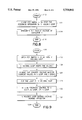
- FIG. 8 Flow diagram showing a method for remembering the output voltage at the V holding loop in the output voltage tracking operation of a fundamental embodiment illustrated in FIG. 1
- FIG. 9 Flow diagram showing a method for changing settings of outputs when the V holding loop is in the output voltage holding operation for a fundamental embodiment illustrated in FIG. 1
- FIG. 1 The fundamental embodiment of the invention is shown in FIG. 1.
- the constituent elements with the same functions as in the prior art circuits are given the same numbers.
- structural elements such as the correction means in the feedback circuits, the range switching, and the current source control parts which perform various kinds of signal processing and control, are omitted.
- the fundamental embodiment of the invention in FIG. 1 is controlled to switch or change various settings of modules by digital control signals. Measurement modules, CPU and control lines for switching and changing various settings of voltage and/or current are also omitted in FIG. 1.
- the fundamental embodiment of the V holding loop is a loop including a capacitor 1 (which is the output of the voltage memory circuit), an error amplifier 3, an FET switch 5, a voltage-current converter 7, integrating circuit 41, power amplifier 42, current ranging circuit 43, and buffer amplifier 45.
- Integrating circuit 41, power amplifier 42, current ranging circuit 43, and buffer amplifier 45 are loop constituent elements which are common to this loop and the V loop, Ip loop, and In loop of the prior art.
- the V holding loop has two states of operation, an output voltage tracking operation and an output voltage holding operation.
- the output voltage holding operation is the operation performed while the control voltage and current values of the device are changed. Its purpose is to hold the output voltage at a constant value.
- the output voltage tracking operation is performed during the ordinary operating state of the device, when the changes made in the device have been completed; and its purpose is to track and remember the output voltage.
- the FET switch 5 In the output voltage tracking operation, the FET switch 5 is closed and the feedback loop of the V holding loop is cut, so that the feedback control operation is stopped.
- FET switch 5 When the control voltage and current values of the measurement device are changed, FET switch 5 is opened, the feedback loop of the V holding loop is activated and the operation is switched to the output voltage holding operation.
- the voltage-current converter 7 of this loop is set with a wider dynamic range of current output than the voltage-current converters of the V loop, Ip loop, and In loop, as shown by the dotted line in FIG. 7. That is, the current value at the time of saturation is set at a value exceeding three times the saturation current (Is) of voltage-current converter 17.
- the V holding loop When the V holding loop forms the feedback loop, the voltage differential between the voltage charge on capacitor 1 and the output voltage of buffer amplifier 45, is input into error amplifier 3.
- the V holding loop is then controlled by feedback, so that it tries to keep the voltage differential at zero.
- the V loop or I loop (which determined the output voltage before this by exercising feedback control) and the V holding loop compete to control the output voltage simultaneously. But, the voltage-current converters of the V loop or I loops, which have smaller dynamic ranges, become saturated first, and ultimately the V holding loop exerts control. Moreover, the error amplifier of the loop, which was performing feedback control, is clamped.
- FIG. 2 shows an example of the invention which has a means for improving the stability of the feedback operation of the V holding loop and eliminates the spikes and overshoots.
- structural elements such as the correction means of the feedback circuits, etc., including the V holding loop, the range switching, and the calculation and control parts which perform various kinds of signal processing and control, are omitted.
- the fundamental embodiment of the invention in FIG. 2 is controlled to switch or change various settings of modules by digital control signals. Measurement modules, CPU and control lines for switching and changing various settings of voltage and/or current are also omitted in FIG. 2.
- a resistance 2 is inserted between capacitor 1 and error amplifier 3 of the V holding loop, and an FET switch 4 is connected in parallel across resistance 2.
- a clamp circuit 6 is connected between the connection point of capacitor 1 and resistance 2 and the output terminal of error amplifier 3.
- FET switches 15, 26, and 36 are connected between the inputs and outputs of the error amplifiers in the V loop, the Ip loop, and the In loop. Their operations are described below.
- Resistor 2 between capacitor 1 and the input of error amplifier 3, is given a value almost equal to feedback resistor 16 of the V loop, improving the stability of the feedback loop of the V holding loop.
- resistor 2 is bypassed by closing FET switch 4, so that no holding delay is produced.
- a clamping circuit 6 is connected to the V holding loop to prevent the FET switches from operating mistakenly during the output voltage holding operation.
Abstract
Description
Claims (13)
Applications Claiming Priority (2)
| Application Number | Priority Date | Filing Date | Title |
|---|---|---|---|
| JP7-086204 | 1995-03-17 | ||
| JP08620495A JP3457091B2 (en) | 1995-03-17 | 1995-03-17 | Voltage-current characteristic measuring device |
Publications (1)
| Publication Number | Publication Date |
|---|---|
| US5754041A true US5754041A (en) | 1998-05-19 |
Family
ID=13880253
Family Applications (1)
| Application Number | Title | Priority Date | Filing Date |
|---|---|---|---|
| US08/616,142 Expired - Fee Related US5754041A (en) | 1995-03-17 | 1996-03-14 | Device for measuring voltage/current characteristics with means to prevent output transients during changes in settings |
Country Status (2)
| Country | Link |
|---|---|
| US (1) | US5754041A (en) |
| JP (1) | JP3457091B2 (en) |
Cited By (24)
| Publication number | Priority date | Publication date | Assignee | Title |
|---|---|---|---|---|
| US5917331A (en) * | 1995-10-23 | 1999-06-29 | Megatest Corporation | Integrated circuit test method and structure |
| US5959463A (en) * | 1997-03-10 | 1999-09-28 | Mitsubishi Denki Kabushiki Kaisha | Semiconductor test apparatus for measuring power supply current of semiconductor device |
| US6137256A (en) * | 1998-11-10 | 2000-10-24 | Tridelta Industries, Inc. | Soft turn-off controller for switched reluctance machines |
| WO2002084314A1 (en) * | 2001-04-12 | 2002-10-24 | Teradyne, Inc. | Apparatus and method for managing automatic transitions between multiple feedback paths |
| US6683462B2 (en) | 2000-11-30 | 2004-01-27 | Agilent Technologies, Inc. | Apparatus for and method of measuring capacitance with high accuracy |
| US20050001283A1 (en) * | 1996-05-30 | 2005-01-06 | Kabushiki Kaisha Toshiba | Semiconductor integrated circuit device and method of testing the same |
| US20060132165A1 (en) * | 2004-12-21 | 2006-06-22 | Ernest Walker | Method and system for testing semiconductor devices |
| US20060132163A1 (en) * | 2004-12-17 | 2006-06-22 | Ernest Walker | Using parametric measurement units as a source of power for a device under test |
| US20060132164A1 (en) * | 2004-12-17 | 2006-06-22 | Ernest Walker | Using a parametric measurement unit to sense a voltage at a device under test |
| US20060132166A1 (en) * | 2004-12-21 | 2006-06-22 | Ernest Walker | Method and system for producing signals to test semiconductor devices |
| US20060279310A1 (en) * | 2004-12-21 | 2006-12-14 | Teradyne, Inc. | Method and system for monitoring test signals for semiconductor devices |
| WO2006071668A3 (en) * | 2004-12-23 | 2007-01-04 | Teradyne Inc | Pin electronics with high voltage functionality |
| US20070069755A1 (en) * | 2005-09-28 | 2007-03-29 | Sartschev Ronald A | Pin electronics driver |
| US20090121908A1 (en) * | 2007-11-08 | 2009-05-14 | Regier Christopher G | Source-Measure Unit Based on Digital Control Loop |
| US20100164463A1 (en) * | 2007-01-26 | 2010-07-01 | Advantest Corporation | Voltage generator with current limiting and semiconductor testing device |
| US20120306518A1 (en) * | 2011-06-06 | 2012-12-06 | Regier Christopher G | Fast Current Saturation Recovery for a Digital Source Measure Unit (SMU) |
| US8456338B2 (en) | 2011-06-06 | 2013-06-04 | National Instruments Corporation | Compliance methods for source measure units operating with digital control loops |
| US8604765B2 (en) | 2011-06-06 | 2013-12-10 | National Instruments Corporation | Resistance simulation and common mode rejection for digital source-measure units |
| US8797025B2 (en) | 2011-06-06 | 2014-08-05 | National Instruments Corporation | Compensation methods for digital source-measure-units (SMUs) |
| WO2016044849A1 (en) * | 2014-09-19 | 2016-03-24 | Elevate Semiconductor, Inc. | Parametric pin measurement unit high voltage extension |
| US9547035B2 (en) | 2014-04-30 | 2017-01-17 | Keysight Technologies, Inc. | System and method for converging current with target current in device under test |
| EP3650868A3 (en) * | 2018-10-17 | 2020-09-02 | Analog Devices Global Unlimited Company | Amplifier systems for measuring a wide range of current |
| CN111638744A (en) * | 2020-04-30 | 2020-09-08 | 北京航天时代光电科技有限公司 | Current frequency conversion circuit |
| US11105843B2 (en) | 2019-10-10 | 2021-08-31 | Analog Devices International Unlimited Company | Robust architecture for mode switching of a force and measure apparatus |
Families Citing this family (5)
| Publication number | Priority date | Publication date | Assignee | Title |
|---|---|---|---|---|
| JP2004219126A (en) | 2003-01-10 | 2004-08-05 | Agilent Technologies Japan Ltd | Method of automatically changing current range |
| JP4832200B2 (en) * | 2006-07-18 | 2011-12-07 | 久元電子股▼ふん▲有限公司 | Device for measuring static parameters of integrated circuits |
| JP5500333B2 (en) * | 2008-11-28 | 2014-05-21 | ワイアイケー株式会社 | DC test equipment and semiconductor test equipment |
| JP2014092370A (en) | 2012-10-31 | 2014-05-19 | Agilent Technologies Inc | Volt-ampere characteristic generator |
| CN109799451B (en) * | 2019-04-16 | 2019-07-12 | 长沙丰灼通讯科技有限公司 | A kind of current testing device on production line |
Citations (1)
| Publication number | Priority date | Publication date | Assignee | Title |
|---|---|---|---|---|
| US5206582A (en) * | 1988-05-18 | 1993-04-27 | Hewlett-Packard Company | Control system for automated parametric test equipment |
-
1995
- 1995-03-17 JP JP08620495A patent/JP3457091B2/en not_active Expired - Fee Related
-
1996
- 1996-03-14 US US08/616,142 patent/US5754041A/en not_active Expired - Fee Related
Patent Citations (1)
| Publication number | Priority date | Publication date | Assignee | Title |
|---|---|---|---|---|
| US5206582A (en) * | 1988-05-18 | 1993-04-27 | Hewlett-Packard Company | Control system for automated parametric test equipment |
Non-Patent Citations (2)
| Title |
|---|
| Hewlett Packard Journal, Oct. 1982, Susumu Takagi et al., pp. 15 20, Programmable Stimulus/Measurement Units Simplify Device Test Setups . * |
| Hewlett-Packard Journal, Oct. 1982, Susumu Takagi et al., pp. 15-20, "Programmable Stimulus/Measurement Units Simplify Device Test Setups". |
Cited By (43)
| Publication number | Priority date | Publication date | Assignee | Title |
|---|---|---|---|---|
| US5917331A (en) * | 1995-10-23 | 1999-06-29 | Megatest Corporation | Integrated circuit test method and structure |
| US20050001283A1 (en) * | 1996-05-30 | 2005-01-06 | Kabushiki Kaisha Toshiba | Semiconductor integrated circuit device and method of testing the same |
| US7549097B2 (en) | 1996-05-30 | 2009-06-16 | Kabushiki Kaisha Toshiba | Semiconductor integrated circuit device and method of testing the same |
| US20070120125A1 (en) * | 1996-05-30 | 2007-05-31 | Kabushiki Kaisha Toshiba | Semiconductor Integrated Circuit Device and Method of Testing the Same |
| US7208759B2 (en) * | 1996-05-30 | 2007-04-24 | Kabushiki Kaisha Toshiba | Semiconductor integrated circuit device and method of testing the same |
| US20070120202A1 (en) * | 1996-05-30 | 2007-05-31 | Kabushiki Kaisha Toshiba | Semiconductor Integrated Circuit Device and Method of Testing the Same |
| US5959463A (en) * | 1997-03-10 | 1999-09-28 | Mitsubishi Denki Kabushiki Kaisha | Semiconductor test apparatus for measuring power supply current of semiconductor device |
| US6137256A (en) * | 1998-11-10 | 2000-10-24 | Tridelta Industries, Inc. | Soft turn-off controller for switched reluctance machines |
| US6683462B2 (en) | 2000-11-30 | 2004-01-27 | Agilent Technologies, Inc. | Apparatus for and method of measuring capacitance with high accuracy |
| WO2002084314A1 (en) * | 2001-04-12 | 2002-10-24 | Teradyne, Inc. | Apparatus and method for managing automatic transitions between multiple feedback paths |
| WO2006066112A2 (en) * | 2004-12-17 | 2006-06-22 | Teradyne, Inc. | Using parametric measurement units as a source of power for a device under test |
| WO2006066112A3 (en) * | 2004-12-17 | 2006-08-17 | Teradyne Inc | Using parametric measurement units as a source of power for a device under test |
| US7403030B2 (en) * | 2004-12-17 | 2008-07-22 | Teradyne, Inc. | Using parametric measurement units as a source of power for a device under test |
| US7271610B2 (en) | 2004-12-17 | 2007-09-18 | Teradyne, Inc. | Using a parametric measurement unit to sense a voltage at a device under test |
| US20060132164A1 (en) * | 2004-12-17 | 2006-06-22 | Ernest Walker | Using a parametric measurement unit to sense a voltage at a device under test |
| US20060132163A1 (en) * | 2004-12-17 | 2006-06-22 | Ernest Walker | Using parametric measurement units as a source of power for a device under test |
| US20060132166A1 (en) * | 2004-12-21 | 2006-06-22 | Ernest Walker | Method and system for producing signals to test semiconductor devices |
| US7256600B2 (en) | 2004-12-21 | 2007-08-14 | Teradyne, Inc. | Method and system for testing semiconductor devices |
| US20060279310A1 (en) * | 2004-12-21 | 2006-12-14 | Teradyne, Inc. | Method and system for monitoring test signals for semiconductor devices |
| US7135881B2 (en) | 2004-12-21 | 2006-11-14 | Teradyne, Inc. | Method and system for producing signals to test semiconductor devices |
| US7508228B2 (en) | 2004-12-21 | 2009-03-24 | Teradyne, Inc. | Method and system for monitoring test signals for semiconductor devices |
| US20060132165A1 (en) * | 2004-12-21 | 2006-06-22 | Ernest Walker | Method and system for testing semiconductor devices |
| CN101084444B (en) * | 2004-12-23 | 2010-11-24 | 泰拉丁公司 | Pin electronics with high voltage functionality |
| WO2006071668A3 (en) * | 2004-12-23 | 2007-01-04 | Teradyne Inc | Pin electronics with high voltage functionality |
| US20070069755A1 (en) * | 2005-09-28 | 2007-03-29 | Sartschev Ronald A | Pin electronics driver |
| US7560947B2 (en) | 2005-09-28 | 2009-07-14 | Teradyne, Inc. | Pin electronics driver |
| US20100164463A1 (en) * | 2007-01-26 | 2010-07-01 | Advantest Corporation | Voltage generator with current limiting and semiconductor testing device |
| US7834607B2 (en) * | 2007-01-26 | 2010-11-16 | Advantest Corporation | Voltage generator with current limiting and semiconductor testing device |
| US7903008B2 (en) * | 2007-11-08 | 2011-03-08 | National Instruments Corporation | Source-measure unit based on digital control loop |
| US20090121908A1 (en) * | 2007-11-08 | 2009-05-14 | Regier Christopher G | Source-Measure Unit Based on Digital Control Loop |
| US20120306518A1 (en) * | 2011-06-06 | 2012-12-06 | Regier Christopher G | Fast Current Saturation Recovery for a Digital Source Measure Unit (SMU) |
| US8456338B2 (en) | 2011-06-06 | 2013-06-04 | National Instruments Corporation | Compliance methods for source measure units operating with digital control loops |
| US8604765B2 (en) | 2011-06-06 | 2013-12-10 | National Instruments Corporation | Resistance simulation and common mode rejection for digital source-measure units |
| US8653840B2 (en) * | 2011-06-06 | 2014-02-18 | National Instruments Corporation | Fast current saturation recovery for a digital source measure unit (SMU) |
| US8797025B2 (en) | 2011-06-06 | 2014-08-05 | National Instruments Corporation | Compensation methods for digital source-measure-units (SMUs) |
| US9547035B2 (en) | 2014-04-30 | 2017-01-17 | Keysight Technologies, Inc. | System and method for converging current with target current in device under test |
| WO2016044849A1 (en) * | 2014-09-19 | 2016-03-24 | Elevate Semiconductor, Inc. | Parametric pin measurement unit high voltage extension |
| CN107003344A (en) * | 2014-09-19 | 2017-08-01 | 艾利维特半导体公司 | Parameter pin measuring unit high voltage extends |
| CN107003344B (en) * | 2014-09-19 | 2019-11-01 | 艾利维特半导体公司 | The extension of parameter pin measuring unit high voltage |
| EP3650868A3 (en) * | 2018-10-17 | 2020-09-02 | Analog Devices Global Unlimited Company | Amplifier systems for measuring a wide range of current |
| US10972063B2 (en) | 2018-10-17 | 2021-04-06 | Analog Devices Global Unlimited Company | Amplifier systems for measuring a wide range of current |
| US11105843B2 (en) | 2019-10-10 | 2021-08-31 | Analog Devices International Unlimited Company | Robust architecture for mode switching of a force and measure apparatus |
| CN111638744A (en) * | 2020-04-30 | 2020-09-08 | 北京航天时代光电科技有限公司 | Current frequency conversion circuit |
Also Published As
| Publication number | Publication date |
|---|---|
| JP3457091B2 (en) | 2003-10-14 |
| JPH08262069A (en) | 1996-10-11 |
Similar Documents
| Publication | Publication Date | Title |
|---|---|---|
| US5754041A (en) | Device for measuring voltage/current characteristics with means to prevent output transients during changes in settings | |
| KR940701546A (en) | Method and device for charging and testing the battery | |
| US6255839B1 (en) | Voltage applied type current measuring circuit in an IC testing apparatus | |
| JPH10132898A (en) | Driver circuit for ic tester | |
| JP3119335B2 (en) | IC test equipment | |
| US6922071B2 (en) | Setting multiple chip parameters using one IC terminal | |
| US6292010B1 (en) | Dynamic pin driver combining high voltage mode and high speed mode | |
| JPS6332379A (en) | Active load network | |
| JPS60105972A (en) | Analog signal measuring apparatus | |
| JP3431053B2 (en) | Timing generator | |
| CA2407766C (en) | Vddq integrated circuit testing system and method | |
| JPH11326441A (en) | Semiconductor testing device | |
| Johnson et al. | A general purpose ATE based I/sub DDQ/measurement circuit | |
| JPH04259868A (en) | Ic tester | |
| JP3057847B2 (en) | Semiconductor integrated circuit | |
| US20060214812A1 (en) | Measurement of output voltage characteristics on dynamic logic signals | |
| JPH06324105A (en) | Semiconductor testing device | |
| JP3178563B2 (en) | Multi-value voltage high-speed comparator | |
| JP4669141B2 (en) | A / D converter | |
| KR100668250B1 (en) | Tristate circuit and method of switching output signal level | |
| JPH08292227A (en) | Terminal circuit | |
| JPH03107779A (en) | Power supply circuit for ic tester measurement | |
| JP2691182B2 (en) | Latch-up measurement method for integrated circuits | |
| JPH07183346A (en) | Semiconductor testing device | |
| JPH07264022A (en) | Programmable delay generator |
Legal Events
| Date | Code | Title | Description |
|---|---|---|---|
| AS | Assignment |
Owner name: HEWLETT-PACKARD COMPANY, CALIFORNIA Free format text: ASSIGNMENT OF ASSIGNORS INTEREST;ASSIGNOR:HEWLETT-PACKARD JAPAN, LTD.;REEL/FRAME:007949/0911 Effective date: 19960313 |
|
| AS | Assignment |
Owner name: HEWLETT-PACKARD COMPANY, A DELAWARE CORPORATION, C Free format text: MERGER;ASSIGNOR:HEWLETT-PACKARD COMPANY, A CALIFORNIA CORPORATION;REEL/FRAME:010841/0649 Effective date: 19980520 |
|
| AS | Assignment |
Owner name: AGILENT TECHNOLOGIES INC, CALIFORNIA Free format text: ASSIGNMENT OF ASSIGNORS INTEREST;ASSIGNOR:HEWLETT-PACKARD COMPANY;REEL/FRAME:010977/0540 Effective date: 19991101 |
|
| FPAY | Fee payment |
Year of fee payment: 4 |
|
| FEPP | Fee payment procedure |
Free format text: PAYOR NUMBER ASSIGNED (ORIGINAL EVENT CODE: ASPN); ENTITY STATUS OF PATENT OWNER: LARGE ENTITY |
|
| REMI | Maintenance fee reminder mailed | ||
| FPAY | Fee payment |
Year of fee payment: 8 |
|
| REMI | Maintenance fee reminder mailed | ||
| LAPS | Lapse for failure to pay maintenance fees | ||
| STCH | Information on status: patent discontinuation |
Free format text: PATENT EXPIRED DUE TO NONPAYMENT OF MAINTENANCE FEES UNDER 37 CFR 1.362 |
|
| FP | Lapsed due to failure to pay maintenance fee |
Effective date: 20100519 |