US5766985A - Process for encapsulating a semiconductor device having a heat sink - Google Patents
Process for encapsulating a semiconductor device having a heat sink Download PDFInfo
- Publication number
- US5766985A US5766985A US08/384,753 US38475395A US5766985A US 5766985 A US5766985 A US 5766985A US 38475395 A US38475395 A US 38475395A US 5766985 A US5766985 A US 5766985A
- Authority
- US
- United States
- Prior art keywords
- plate
- resin
- edge
- positioning
- opposite
- Prior art date
- Legal status (The legal status is an assumption and is not a legal conclusion. Google has not performed a legal analysis and makes no representation as to the accuracy of the status listed.)
- Expired - Lifetime
Links
Images


Classifications
-
- H—ELECTRICITY
- H01—ELECTRIC ELEMENTS
- H01L—SEMICONDUCTOR DEVICES NOT COVERED BY CLASS H10
- H01L21/00—Processes or apparatus adapted for the manufacture or treatment of semiconductor or solid state devices or of parts thereof
- H01L21/02—Manufacture or treatment of semiconductor devices or of parts thereof
- H01L21/04—Manufacture or treatment of semiconductor devices or of parts thereof the devices having at least one potential-jump barrier or surface barrier, e.g. PN junction, depletion layer or carrier concentration layer
- H01L21/50—Assembly of semiconductor devices using processes or apparatus not provided for in a single one of the subgroups H01L21/06 - H01L21/326, e.g. sealing of a cap to a base of a container
- H01L21/56—Encapsulations, e.g. encapsulation layers, coatings
- H01L21/565—Moulds
-
- B—PERFORMING OPERATIONS; TRANSPORTING
- B29—WORKING OF PLASTICS; WORKING OF SUBSTANCES IN A PLASTIC STATE IN GENERAL
- B29C—SHAPING OR JOINING OF PLASTICS; SHAPING OF MATERIAL IN A PLASTIC STATE, NOT OTHERWISE PROVIDED FOR; AFTER-TREATMENT OF THE SHAPED PRODUCTS, e.g. REPAIRING
- B29C45/00—Injection moulding, i.e. forcing the required volume of moulding material through a nozzle into a closed mould; Apparatus therefor
- B29C45/14—Injection moulding, i.e. forcing the required volume of moulding material through a nozzle into a closed mould; Apparatus therefor incorporating preformed parts or layers, e.g. injection moulding around inserts or for coating articles
- B29C45/14065—Positioning or centering articles in the mould
- B29C45/14073—Positioning or centering articles in the mould using means being retractable during injection
-
- H—ELECTRICITY
- H01—ELECTRIC ELEMENTS
- H01L—SEMICONDUCTOR DEVICES NOT COVERED BY CLASS H10
- H01L23/00—Details of semiconductor or other solid state devices
- H01L23/48—Arrangements for conducting electric current to or from the solid state body in operation, e.g. leads, terminal arrangements ; Selection of materials therefor
- H01L23/488—Arrangements for conducting electric current to or from the solid state body in operation, e.g. leads, terminal arrangements ; Selection of materials therefor consisting of soldered or bonded constructions
- H01L23/495—Lead-frames or other flat leads
- H01L23/49503—Lead-frames or other flat leads characterised by the die pad
-
- H—ELECTRICITY
- H01—ELECTRIC ELEMENTS
- H01L—SEMICONDUCTOR DEVICES NOT COVERED BY CLASS H10
- H01L23/00—Details of semiconductor or other solid state devices
- H01L23/48—Arrangements for conducting electric current to or from the solid state body in operation, e.g. leads, terminal arrangements ; Selection of materials therefor
- H01L23/488—Arrangements for conducting electric current to or from the solid state body in operation, e.g. leads, terminal arrangements ; Selection of materials therefor consisting of soldered or bonded constructions
- H01L23/495—Lead-frames or other flat leads
- H01L23/49541—Geometry of the lead-frame
- H01L23/49562—Geometry of the lead-frame for devices being provided for in H01L29/00
-
- B—PERFORMING OPERATIONS; TRANSPORTING
- B29—WORKING OF PLASTICS; WORKING OF SUBSTANCES IN A PLASTIC STATE IN GENERAL
- B29C—SHAPING OR JOINING OF PLASTICS; SHAPING OF MATERIAL IN A PLASTIC STATE, NOT OTHERWISE PROVIDED FOR; AFTER-TREATMENT OF THE SHAPED PRODUCTS, e.g. REPAIRING
- B29C45/00—Injection moulding, i.e. forcing the required volume of moulding material through a nozzle into a closed mould; Apparatus therefor
- B29C45/14—Injection moulding, i.e. forcing the required volume of moulding material through a nozzle into a closed mould; Apparatus therefor incorporating preformed parts or layers, e.g. injection moulding around inserts or for coating articles
- B29C45/14065—Positioning or centering articles in the mould
- B29C2045/14147—Positioning or centering articles in the mould using pins or needles penetrating through the insert
-
- H—ELECTRICITY
- H01—ELECTRIC ELEMENTS
- H01L—SEMICONDUCTOR DEVICES NOT COVERED BY CLASS H10
- H01L2224/00—Indexing scheme for arrangements for connecting or disconnecting semiconductor or solid-state bodies and methods related thereto as covered by H01L24/00
- H01L2224/01—Means for bonding being attached to, or being formed on, the surface to be connected, e.g. chip-to-package, die-attach, "first-level" interconnects; Manufacturing methods related thereto
- H01L2224/42—Wire connectors; Manufacturing methods related thereto
- H01L2224/47—Structure, shape, material or disposition of the wire connectors after the connecting process
- H01L2224/48—Structure, shape, material or disposition of the wire connectors after the connecting process of an individual wire connector
- H01L2224/4805—Shape
- H01L2224/4809—Loop shape
- H01L2224/48091—Arched
-
- H—ELECTRICITY
- H01—ELECTRIC ELEMENTS
- H01L—SEMICONDUCTOR DEVICES NOT COVERED BY CLASS H10
- H01L2224/00—Indexing scheme for arrangements for connecting or disconnecting semiconductor or solid-state bodies and methods related thereto as covered by H01L24/00
- H01L2224/01—Means for bonding being attached to, or being formed on, the surface to be connected, e.g. chip-to-package, die-attach, "first-level" interconnects; Manufacturing methods related thereto
- H01L2224/42—Wire connectors; Manufacturing methods related thereto
- H01L2224/47—Structure, shape, material or disposition of the wire connectors after the connecting process
- H01L2224/48—Structure, shape, material or disposition of the wire connectors after the connecting process of an individual wire connector
- H01L2224/481—Disposition
- H01L2224/48151—Connecting between a semiconductor or solid-state body and an item not being a semiconductor or solid-state body, e.g. chip-to-substrate, chip-to-passive
- H01L2224/48221—Connecting between a semiconductor or solid-state body and an item not being a semiconductor or solid-state body, e.g. chip-to-substrate, chip-to-passive the body and the item being stacked
- H01L2224/48245—Connecting between a semiconductor or solid-state body and an item not being a semiconductor or solid-state body, e.g. chip-to-substrate, chip-to-passive the body and the item being stacked the item being metallic
- H01L2224/48247—Connecting between a semiconductor or solid-state body and an item not being a semiconductor or solid-state body, e.g. chip-to-substrate, chip-to-passive the body and the item being stacked the item being metallic connecting the wire to a bond pad of the item
-
- H—ELECTRICITY
- H01—ELECTRIC ELEMENTS
- H01L—SEMICONDUCTOR DEVICES NOT COVERED BY CLASS H10
- H01L2224/00—Indexing scheme for arrangements for connecting or disconnecting semiconductor or solid-state bodies and methods related thereto as covered by H01L24/00
- H01L2224/01—Means for bonding being attached to, or being formed on, the surface to be connected, e.g. chip-to-package, die-attach, "first-level" interconnects; Manufacturing methods related thereto
- H01L2224/42—Wire connectors; Manufacturing methods related thereto
- H01L2224/47—Structure, shape, material or disposition of the wire connectors after the connecting process
- H01L2224/48—Structure, shape, material or disposition of the wire connectors after the connecting process of an individual wire connector
- H01L2224/484—Connecting portions
- H01L2224/4847—Connecting portions the connecting portion on the bonding area of the semiconductor or solid-state body being a wedge bond
- H01L2224/48472—Connecting portions the connecting portion on the bonding area of the semiconductor or solid-state body being a wedge bond the other connecting portion not on the bonding area also being a wedge bond, i.e. wedge-to-wedge
-
- H—ELECTRICITY
- H01—ELECTRIC ELEMENTS
- H01L—SEMICONDUCTOR DEVICES NOT COVERED BY CLASS H10
- H01L2224/00—Indexing scheme for arrangements for connecting or disconnecting semiconductor or solid-state bodies and methods related thereto as covered by H01L24/00
- H01L2224/01—Means for bonding being attached to, or being formed on, the surface to be connected, e.g. chip-to-package, die-attach, "first-level" interconnects; Manufacturing methods related thereto
- H01L2224/42—Wire connectors; Manufacturing methods related thereto
- H01L2224/47—Structure, shape, material or disposition of the wire connectors after the connecting process
- H01L2224/49—Structure, shape, material or disposition of the wire connectors after the connecting process of a plurality of wire connectors
- H01L2224/491—Disposition
- H01L2224/4912—Layout
- H01L2224/49171—Fan-out arrangements
-
- H—ELECTRICITY
- H01—ELECTRIC ELEMENTS
- H01L—SEMICONDUCTOR DEVICES NOT COVERED BY CLASS H10
- H01L24/00—Arrangements for connecting or disconnecting semiconductor or solid-state bodies; Methods or apparatus related thereto
- H01L24/01—Means for bonding being attached to, or being formed on, the surface to be connected, e.g. chip-to-package, die-attach, "first-level" interconnects; Manufacturing methods related thereto
- H01L24/42—Wire connectors; Manufacturing methods related thereto
- H01L24/47—Structure, shape, material or disposition of the wire connectors after the connecting process
- H01L24/48—Structure, shape, material or disposition of the wire connectors after the connecting process of an individual wire connector
-
- H—ELECTRICITY
- H01—ELECTRIC ELEMENTS
- H01L—SEMICONDUCTOR DEVICES NOT COVERED BY CLASS H10
- H01L24/00—Arrangements for connecting or disconnecting semiconductor or solid-state bodies; Methods or apparatus related thereto
- H01L24/01—Means for bonding being attached to, or being formed on, the surface to be connected, e.g. chip-to-package, die-attach, "first-level" interconnects; Manufacturing methods related thereto
- H01L24/42—Wire connectors; Manufacturing methods related thereto
- H01L24/47—Structure, shape, material or disposition of the wire connectors after the connecting process
- H01L24/49—Structure, shape, material or disposition of the wire connectors after the connecting process of a plurality of wire connectors
-
- H—ELECTRICITY
- H01—ELECTRIC ELEMENTS
- H01L—SEMICONDUCTOR DEVICES NOT COVERED BY CLASS H10
- H01L2924/00—Indexing scheme for arrangements or methods for connecting or disconnecting semiconductor or solid-state bodies as covered by H01L24/00
- H01L2924/0001—Technical content checked by a classifier
- H01L2924/00014—Technical content checked by a classifier the subject-matter covered by the group, the symbol of which is combined with the symbol of this group, being disclosed without further technical details
-
- H—ELECTRICITY
- H01—ELECTRIC ELEMENTS
- H01L—SEMICONDUCTOR DEVICES NOT COVERED BY CLASS H10
- H01L2924/00—Indexing scheme for arrangements or methods for connecting or disconnecting semiconductor or solid-state bodies as covered by H01L24/00
- H01L2924/10—Details of semiconductor or other solid state devices to be connected
- H01L2924/11—Device type
- H01L2924/13—Discrete devices, e.g. 3 terminal devices
- H01L2924/1301—Thyristor
- H01L2924/13033—TRIAC - Triode for Alternating Current - A bidirectional switching device containing two thyristor structures with common gate contact
-
- H—ELECTRICITY
- H01—ELECTRIC ELEMENTS
- H01L—SEMICONDUCTOR DEVICES NOT COVERED BY CLASS H10
- H01L2924/00—Indexing scheme for arrangements or methods for connecting or disconnecting semiconductor or solid-state bodies as covered by H01L24/00
- H01L2924/10—Details of semiconductor or other solid state devices to be connected
- H01L2924/11—Device type
- H01L2924/13—Discrete devices, e.g. 3 terminal devices
- H01L2924/1304—Transistor
- H01L2924/1305—Bipolar Junction Transistor [BJT]
-
- H—ELECTRICITY
- H01—ELECTRIC ELEMENTS
- H01L—SEMICONDUCTOR DEVICES NOT COVERED BY CLASS H10
- H01L2924/00—Indexing scheme for arrangements or methods for connecting or disconnecting semiconductor or solid-state bodies as covered by H01L24/00
- H01L2924/10—Details of semiconductor or other solid state devices to be connected
- H01L2924/11—Device type
- H01L2924/14—Integrated circuits
-
- H—ELECTRICITY
- H01—ELECTRIC ELEMENTS
- H01L—SEMICONDUCTOR DEVICES NOT COVERED BY CLASS H10
- H01L2924/00—Indexing scheme for arrangements or methods for connecting or disconnecting semiconductor or solid-state bodies as covered by H01L24/00
- H01L2924/15—Details of package parts other than the semiconductor or other solid state devices to be connected
- H01L2924/181—Encapsulation
- H01L2924/1815—Shape
Definitions
- the present invention relates to packaged semiconductor devices and to methods for packaging, and particularly to resin-encapsulated and fully insulated packages for discrete or integrated devices.
- ISOWATT-218 package generally shown in FIG. 1, and various similar packages. These include ISOWATT-220 packages, as well as ISOWATT-221 and others. See the SGS-Thompson databooks on POWER BIPOLAR TRANSISTORS (1.ed. 1989), and SCRs AND TRIACS (2nd ed. 1991), both of which are hereby incorporated by reference.
- This type of package has a through-hole tab which can be used to achieve good thermal conductivity (by bolting this tab to a heat sink).
- the disclosed innovations will be described with specific reference to this type of package, but are not strictly limited to such packages.
- the disclosed inventions advantageously provide an electrically insulated plastic device completely surrounded by resin which is obtainable by a more tolerant manufacturing process than in the prior art.
- a further advantage is a process for manufacturing defect-free plastic devices with a high level of reliability without increasing manufacturing costs.
- the semiconductor device in the present invention comprises a resin enclosure and a metal plate surrounded by the enclosure. Onto this plate is brazed a semiconductor chip, on one end of which there is an external connector and on the other end a through hole. This through hole allows the attachment of the device to an external support and/or heat sink.
- the plate outline has on a second side, opposite that which leads to the connector, a recess. This recess, in its innermost part, radious with said hole in the plate; and this recess displays an extension mouth not smaller than the diameter of said hole.
- the plate has on the two remaining sides additional lateral indentations extending for at least one third of their length, and the plate surface opposite the side that supports the semiconductor chip has a step transition between first and second planar portions.
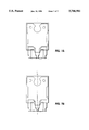
- FIG. 1 shows an isometric view of an electrically insulated device in accordance with the known art.
- FIGS. 2a-2c show schematically some phases of a known encapsulation process
- FIGS. 3a-3b show a top and a cross section view not in scale of the device of FIG. 1.
- FIGS. 4a-4e show a top and various cross section views of a device in the present invention.
- FIGS. 5a-5d show a top view and side view of the flow lines of the resin inside the cavity of the die during the encapsulation process in the present invention and in the prior art respectively.
- FIGS. 6a-6f show cross sections of some encapsulation process phases for the metal plate positioning system in the present invention.
- FIGS. 7a-7b show a top view of the metal plate in the present invention after and before centering.
- FIGS. 1, 2a-2c and 3a-3b represent an example of a known encapsulation process and the device obtained.
- the device (see FIGS. 1 and 3) comprises a metal plate (2) surrounded by a resin enclosure (3).
- a semiconductor chip (4) is affixed to the metal plate (2), by brazing alloy.
- Metal terminals (5a, 5b) are surrounded partly by the resin body (3) and are electrically connected to the plate (2) by wires (6).
- the central terminal (5) is an extension of the plate and acts as the transistor collector.
- a through hole (7) both in the metal plate and in the resin body allows attachment of the device to a suitable external support or heat sink. Electrical insulation of the device is provided by the same resin (3) which completely surrounds the metal plate (2), covering its lower surface with a thin insulating layer (8).
- FIGS. 2a-2c illustrate some steps of a known process.
- the metal plate of the device the central terminal and the semiconductor chip are indicated by 31, 38 and 33 respectively.
- These steps call for positioning the plate in the cavity of a die (41/42), by means of retractable pins (43, 44) and the injection of resin through a duct (47, FIG. 2a).
- the pins (43, 44) are retracted and injection of resin is continued to fill the cavities left by the pins (FIG. 2b).
- the package obtained is extracted from the die by use of the positioning pins (43, 44) and knockout pins (45, 46).
- the resin is injected at high pressure during the transfer molding process: Insulation obtained from the molding resin calls for a low defect level. This is especially true of the thin resin layer under the metal plate which must withstand high voltages. The low defect requirement, and the high hydrodynamic resistance encountered by the resin during injection into the die cavity, makes it necessary to use high resin injection pressure during the molding process.
- the plate may be found to be improperly spaced from the die wall, or even touching them. Because of the critical nature of plate position, this can lead to loss of electrical insulation.
- FIGS. 4a-4d illustrate the structure of a device according to the presently preferred embodiment. This embodiment includes the following features:
- the hole (24) in the metal plate is open opposite the input slot of the resin in the die cavity (the position of this slot is indicated by 11 in FIG. 4a).
- two lateral indentations (12) are present in the plate in the region where the semiconductor chip is present,
- the plate surface opposite that to which leads the central connector, includes a discontinuity of height 17 (visible, in alternative embodiments, in FIGS. 4b and 4e, near item 18). This discontinuity can be created be milling or bending.
- grooves (14) are found on the back of the plate in the region (16)(covered by a thin layer of resin). These grooves are parallel with the lateral indentations (12) described earlier.
- Lateral indentations (12) increase the distance (15) between the plate (9) and the walls of the die (13). These indentations also allow an increased flow of resin into the thin insulation layer (16); this allows formation of the insulation layer (16) by resin flows from two directions. The resin flows not only parallel to the layer (16), but also perpendicularly (through the lateral indentations 12). The opening (10) and the lateral indentations (12) allow better die filling with low pressures. Once the resin has solidified, these features create a hook (15 and 15a) where the plate and the resin meet. This hook (15 and 15a) strengthens the structure by reducing the stresses which the solid resin places on the semiconductor chip.
- Longitudinal channels (14) facilitate the creation of the layer (16) by allowing better resin flow. Moreover, the surface area added by these channels improves adhesion between the resin layer (16) and the metal plate (9). These improvements assist in avoiding the creation of defects (porousness of the resin, nonuniformity of the layer, etc.) which cause electrical insulation alterations.
- these channels increase the contact surface area and act as hooks between the resin layer (16) and the plate (9) to improve adhesion between these two materials.
- FIGS. 5a-5d show top and side views of the flow lines of the resin in the die cavity during the encapsulation process in the present invention (5a) and the prior art (5b) respectively.
- the figures confirm the inventive solutions described above by showing increased resin flow in the die cavity and facilitated filling of the die cavity on the side under the plate.
- FIGS. 6a-6f illustrate some steps of an encapsulation process in the present invention that are designed to ensure correct horizontal positioning of the, metal plate inside the die cavity.
- the figures show a die cavity cross section along a plane through the axes of the two pins nearest the package fixing hole. (The hole is not shown so the diagram will be easier to view.)
- the positioning pins (20) with tapered ends (19) make contact with the plate (9) to position it in the die.
- the tapered end shown forms an angle of approximately 70 degrees.
- the plate are two through holes (18) having diameter equal to the base of the tapered points.
- the centering system will position the plate correctly in the cavity (FIGS. 6c and 7a), holding it in the correct position during the entire molding process.
- FIG. 6a represents the moment when the plate (9) is placed in the cavity (22) of the die in an off center position.
- FIG. 6b shows the pins in the positioning process.
- the tapered point (19) of the pins acts on the hole (18), moving the plate inside the die cavity and thereby centering it perfectly.
- FIG. 6c shows the system with the plate correctly positioned at the beginning of filling.
- the diameter of the base of the tapered point less than the diameter of the pins creates an annular surface on which the centered plate rests. This prevents vertical movement of the plate.
- FIG. 6d shows the die cavity filled with resin with the plate correctly centered.
- FIG. 6e shows the phase where the pins are withdrawn and the resin continues to flow to fill the cavity (23) left by the pins and the through holes (18).
- FIG. 6f shows the die cavity entirely filled with resin already solidified with the semiconductor device and the metal plate correctly centered. At this time, it is ready to be knocked out in accordance with prior known procedure.
- the tapered pin system instead of being provided on the top of the die could be provided on the bottom of the die;
- the tapered pin system could be provided both on the top and the bottom.
- the through holes 18 can alternatively be blind, as long as their depth was equal to or greater than the height of the tapered point of the pin. In this case, too, these holes still fulfill the functions of centering as set forth above.
- the positioning holes whether through or blind, to be noncircular, e.g. elliptical, as shown in FIGS. 7a and 7b.
- the hole have a shape to allow penetration of only the tapered point and not the rest of the pin.
- elliptical holes they must have their major axis parallel to the axis of the central connector and their minor axis of a length equal to the diameter of the base of the tapered point of the pins.
- the elliptical holes display the advantage, in comparison with round holes, of permitting input of the resin when the pins are in fully inserted position (position of FIG. 6d).
- the device with three terminals described can be generalized for other packages completely surrounded by resin and electrically insulated.
- the device in the present invention can have more than three metal terminals as would be found in integrated circuits.
- the present invention is not limited solely to packaging of three-terminal devices, but can also be used for packaging of two- and four-terminal devices.
Abstract
Description
Claims (18)
Priority Applications (1)
| Application Number | Priority Date | Filing Date | Title |
|---|---|---|---|
| US08/384,753 US5766985A (en) | 1991-12-05 | 1995-02-06 | Process for encapsulating a semiconductor device having a heat sink |
Applications Claiming Priority (4)
| Application Number | Priority Date | Filing Date | Title |
|---|---|---|---|
| ITMI91A3266 | 1991-12-05 | ||
| ITMI913266A IT1252624B (en) | 1991-12-05 | 1991-12-05 | SEMICONDUCTOR RESIN ENCLOSED AND ELECTRICALLY INSULATED DEVICE WITH IMPROVED INSULATION CHARACTERISTICS, AND RELATED MANUFACTURING PROCESS |
| US07/987,490 US5514913A (en) | 1991-12-05 | 1992-12-07 | Resin-encapsulated semiconductor device having improved adhesion |
| US08/384,753 US5766985A (en) | 1991-12-05 | 1995-02-06 | Process for encapsulating a semiconductor device having a heat sink |
Related Parent Applications (1)
| Application Number | Title | Priority Date | Filing Date |
|---|---|---|---|
| US07/987,490 Division US5514913A (en) | 1991-12-05 | 1992-12-07 | Resin-encapsulated semiconductor device having improved adhesion |
Publications (1)
| Publication Number | Publication Date |
|---|---|
| US5766985A true US5766985A (en) | 1998-06-16 |
Family
ID=11361268
Family Applications (2)
| Application Number | Title | Priority Date | Filing Date |
|---|---|---|---|
| US07/987,490 Expired - Lifetime US5514913A (en) | 1991-12-05 | 1992-12-07 | Resin-encapsulated semiconductor device having improved adhesion |
| US08/384,753 Expired - Lifetime US5766985A (en) | 1991-12-05 | 1995-02-06 | Process for encapsulating a semiconductor device having a heat sink |
Family Applications Before (1)
| Application Number | Title | Priority Date | Filing Date |
|---|---|---|---|
| US07/987,490 Expired - Lifetime US5514913A (en) | 1991-12-05 | 1992-12-07 | Resin-encapsulated semiconductor device having improved adhesion |
Country Status (5)
| Country | Link |
|---|---|
| US (2) | US5514913A (en) |
| EP (1) | EP0545487B1 (en) |
| JP (1) | JP3338490B2 (en) |
| DE (1) | DE69221440T2 (en) |
| IT (1) | IT1252624B (en) |
Cited By (18)
| Publication number | Priority date | Publication date | Assignee | Title |
|---|---|---|---|---|
| US5935502A (en) * | 1996-06-28 | 1999-08-10 | Sgs-Thomson Microelectronics | Method for manufacturing plastic package for electronic device having a fully insulated dissipator |
| US6043111A (en) * | 1996-07-30 | 2000-03-28 | Nec Corporation | Small size semiconductor package |
| US6638595B2 (en) * | 2000-06-28 | 2003-10-28 | Micron Technology, Inc. | Method and apparatus for reduced flash encapsulation of microelectronic devices |
| US6645416B2 (en) * | 2000-05-12 | 2003-11-11 | Alstom Ltd. | Insulation of stator windings by injection molding |
| EP1421837A1 (en) * | 2001-08-10 | 2004-05-26 | BLACK & DECKER INC. | Electrically isolated module |
| US6923632B2 (en) * | 1995-05-19 | 2005-08-02 | Denso Corporation | Method and apparatus for forming a casting which includes an insert |
| WO2007012911A1 (en) * | 2005-07-28 | 2007-02-01 | Infineon Technologies Ag | Semiconductor module for a switched-mode power supply and method for its assembly |
| WO2008021290A2 (en) | 2006-08-09 | 2008-02-21 | Homestead Clinical Corporation | Organ-specific proteins and methods of their use |
| CN100468669C (en) * | 2003-12-08 | 2009-03-11 | 半导体元件工业有限责任公司 | Method of forming a semiconductor package and leadframe therefor |
| US20090212446A1 (en) * | 2008-02-25 | 2009-08-27 | Chai Wei Heng | Semiconductor Device |
| EP2051300A3 (en) * | 2007-10-15 | 2009-12-09 | Power Integrations, Inc. | Package for a power semiconductor device |
| US20100025828A1 (en) * | 2008-07-30 | 2010-02-04 | Sanyo Electric Co., Ltd. | Semiconductor device, semiconductor module, method for manufacturing semiconductor device, and lead frame |
| JP2010103279A (en) * | 2008-10-23 | 2010-05-06 | Shindengen Electric Mfg Co Ltd | Semiconductor device |
| WO2010066410A1 (en) * | 2008-12-11 | 2010-06-17 | Trw Automotive Gmbh | Method and mold for producing an electronic component having a plastic insert molded carrier |
| US20110097432A1 (en) * | 2009-10-23 | 2011-04-28 | Hon Hai Precision Industry Co., Ltd. | Injection mold |
| CN106601714A (en) * | 2017-01-25 | 2017-04-26 | 长电科技(宿迁)有限公司 | Insulation package structure in movable ejector pin and process method thereof |
| US10232531B1 (en) * | 2014-07-08 | 2019-03-19 | Verily Life Sciences Llc | Methods and apparatus for forming a polymer layer around a structure using a plurality of protrusions |
| US11198237B2 (en) * | 2016-05-25 | 2021-12-14 | Olympus Corporation | Insert molding method |
Families Citing this family (15)
| Publication number | Priority date | Publication date | Assignee | Title |
|---|---|---|---|---|
| DE4340862C2 (en) * | 1993-12-01 | 2002-04-11 | Vishay Semiconductor Gmbh | Potting device for the production of optoelectronic components |
| JPH08204099A (en) * | 1995-01-31 | 1996-08-09 | Rohm Co Ltd | Constitution of semiconductor device and its forming method |
| EP0782184A1 (en) * | 1995-12-29 | 1997-07-02 | STMicroelectronics S.r.l. | Heat dissipating and supporting structure for a package |
| US5793613A (en) * | 1995-12-29 | 1998-08-11 | Sgs-Thomson Microelectronics S.R.1. | Heat-dissipating and supporting structure for a plastic package with a fully insulated heat sink for an electronic device |
| FR2844219B1 (en) * | 2002-09-09 | 2004-10-22 | Valeo Electronique Sys Liaison | OVER-MOLDING MOLD |
| US8334583B2 (en) * | 2005-07-20 | 2012-12-18 | Infineon Technologies Ag | Leadframe strip and mold apparatus for an electronic component and method of encapsulating an electronic component |
| WO2007074352A1 (en) * | 2005-12-29 | 2007-07-05 | Infineon Technologies Ag | Electronic component and a method of fabricating an electronic component |
| WO2011057662A1 (en) * | 2009-11-11 | 2011-05-19 | Datalogic Automation S.R.L. | Method for injection moulding an external housing of an object, object and apparatus for injection moulding |
| JP5549491B2 (en) * | 2010-09-06 | 2014-07-16 | 日立金属株式会社 | Busbar module manufacturing method and busbar module |
| US20160277017A1 (en) * | 2011-09-13 | 2016-09-22 | Fsp Technology Inc. | Snubber circuit |
| JP6162643B2 (en) | 2014-05-21 | 2017-07-12 | 三菱電機株式会社 | Semiconductor device |
| FR3046903B1 (en) * | 2016-01-19 | 2019-08-16 | Valeo Comfort And Driving Assistance | ELECTRONIC SEALED DEVICE AND METHOD FOR OBTAINING THE SAME |
| JP6448712B2 (en) * | 2017-06-15 | 2019-01-09 | 三菱電機株式会社 | Semiconductor device |
| JP6888525B2 (en) * | 2017-11-06 | 2021-06-16 | 株式会社デンソー | Manufacturing method of energizing member module |
| EP3916910B1 (en) | 2020-05-26 | 2022-12-14 | Premo, S.A. | Long range low frequency antenna |
Citations (29)
| Publication number | Priority date | Publication date | Assignee | Title |
|---|---|---|---|---|
| US3715423A (en) * | 1971-01-25 | 1973-02-06 | Motorola Inc | Plastic encapsulation of semiconductor devices |
| JPS5238885A (en) * | 1975-09-22 | 1977-03-25 | Nec Home Electronics Ltd | Method for production of semiconductor device |
| JPS5565450A (en) * | 1978-11-10 | 1980-05-16 | Hitachi Ltd | Resin-mold type semiconductor device |
| US4266267A (en) * | 1979-11-19 | 1981-05-05 | General Electric Company | Mounting arrangement for transistors and the like |
| WO1982003294A1 (en) * | 1981-03-23 | 1982-09-30 | Inc Motorola | Semiconductor device including plateless package |
| JPS5917273A (en) * | 1982-07-20 | 1984-01-28 | Nec Corp | Resin sealed semiconductor device |
| EP0121374A1 (en) * | 1983-03-30 | 1984-10-10 | Era Patents Limited | Mounting of semi-conductor devices |
| JPS60242649A (en) * | 1985-03-29 | 1985-12-02 | Hitachi Ltd | Resin sealed semiconductor device |
| JPS6156420A (en) * | 1984-07-31 | 1986-03-22 | Sanken Electric Co Ltd | Manufacture of resin-sealed semiconductor device |
| JPS6180845A (en) * | 1984-09-28 | 1986-04-24 | Hitachi Ltd | Semiconductor device |
| JPS6193652A (en) * | 1985-09-06 | 1986-05-12 | Hitachi Ltd | Resin seal type semiconductor device |
| JPS61102040A (en) * | 1984-10-25 | 1986-05-20 | Sanken Electric Co Ltd | Manufacture of resin seal type semiconductor device |
| JPS61219144A (en) * | 1985-03-25 | 1986-09-29 | Sanken Electric Co Ltd | Manufacture of resin sealed type semiconductor device |
| JPS62154656A (en) * | 1985-12-27 | 1987-07-09 | Toshiba Corp | Manufacture of resin-sealed semiconductor device |
| JPS6366953A (en) * | 1986-09-08 | 1988-03-25 | Toshiba Corp | Polymer planar-metallization type semiconductor device and manufacture threrof |
| JPS6378558A (en) * | 1986-09-22 | 1988-04-08 | Hitachi Ltd | Electronic device |
| JPS63170949A (en) * | 1987-01-09 | 1988-07-14 | Fuji Electric Co Ltd | Semiconductor device |
| JPS63208255A (en) * | 1987-02-25 | 1988-08-29 | Hitachi Ltd | Electronic device |
| JPS63213362A (en) * | 1987-02-27 | 1988-09-06 | Mitsubishi Electric Corp | Resin sealed semiconductor device |
| JPS6442844A (en) * | 1987-08-10 | 1989-02-15 | Fuji Electric Co Ltd | Lead frame for semiconductor device |
| US4835423A (en) * | 1986-11-21 | 1989-05-30 | Thomson Semiconducteurs | MOS technology voltage switch-over circuit |
| JPH01258452A (en) * | 1988-04-08 | 1989-10-16 | Nec Corp | Resin-sealed semiconductor device |
| US4888307A (en) * | 1986-08-27 | 1989-12-19 | Sgs Microelettronica S.P.A. | Method for manufacturing plastic encapsulated semiconductor devices |
| JPH01315147A (en) * | 1989-04-07 | 1989-12-20 | Sanken Electric Co Ltd | Manufacture of resin-sealed type semiconductor device |
| JPH02268457A (en) * | 1989-04-10 | 1990-11-02 | Nec Corp | Resin sealed type semiconductor device |
| JPH0353551A (en) * | 1989-07-21 | 1991-03-07 | Nec Corp | Insulated heat sink for semiconductor device |
| JPH0360146A (en) * | 1989-07-28 | 1991-03-15 | Nec Kansai Ltd | Resin mold type semiconductor device and resin molding equipment |
| US5063434A (en) * | 1989-09-22 | 1991-11-05 | Kabushiki Kaisha Toshiba | Plastic molded type power semiconductor device |
| US5105259A (en) * | 1990-09-28 | 1992-04-14 | Motorola, Inc. | Thermally enhanced semiconductor device utilizing a vacuum to ultimately enhance thermal dissipation |
-
1991
- 1991-12-05 IT ITMI913266A patent/IT1252624B/en active IP Right Grant
-
1992
- 1992-11-25 JP JP31519692A patent/JP3338490B2/en not_active Expired - Fee Related
- 1992-11-27 EP EP92203676A patent/EP0545487B1/en not_active Expired - Lifetime
- 1992-11-27 DE DE69221440T patent/DE69221440T2/en not_active Expired - Fee Related
- 1992-12-07 US US07/987,490 patent/US5514913A/en not_active Expired - Lifetime
-
1995
- 1995-02-06 US US08/384,753 patent/US5766985A/en not_active Expired - Lifetime
Patent Citations (29)
| Publication number | Priority date | Publication date | Assignee | Title |
|---|---|---|---|---|
| US3715423A (en) * | 1971-01-25 | 1973-02-06 | Motorola Inc | Plastic encapsulation of semiconductor devices |
| JPS5238885A (en) * | 1975-09-22 | 1977-03-25 | Nec Home Electronics Ltd | Method for production of semiconductor device |
| JPS5565450A (en) * | 1978-11-10 | 1980-05-16 | Hitachi Ltd | Resin-mold type semiconductor device |
| US4266267A (en) * | 1979-11-19 | 1981-05-05 | General Electric Company | Mounting arrangement for transistors and the like |
| WO1982003294A1 (en) * | 1981-03-23 | 1982-09-30 | Inc Motorola | Semiconductor device including plateless package |
| JPS5917273A (en) * | 1982-07-20 | 1984-01-28 | Nec Corp | Resin sealed semiconductor device |
| EP0121374A1 (en) * | 1983-03-30 | 1984-10-10 | Era Patents Limited | Mounting of semi-conductor devices |
| JPS6156420A (en) * | 1984-07-31 | 1986-03-22 | Sanken Electric Co Ltd | Manufacture of resin-sealed semiconductor device |
| JPS6180845A (en) * | 1984-09-28 | 1986-04-24 | Hitachi Ltd | Semiconductor device |
| JPS61102040A (en) * | 1984-10-25 | 1986-05-20 | Sanken Electric Co Ltd | Manufacture of resin seal type semiconductor device |
| JPS61219144A (en) * | 1985-03-25 | 1986-09-29 | Sanken Electric Co Ltd | Manufacture of resin sealed type semiconductor device |
| JPS60242649A (en) * | 1985-03-29 | 1985-12-02 | Hitachi Ltd | Resin sealed semiconductor device |
| JPS6193652A (en) * | 1985-09-06 | 1986-05-12 | Hitachi Ltd | Resin seal type semiconductor device |
| JPS62154656A (en) * | 1985-12-27 | 1987-07-09 | Toshiba Corp | Manufacture of resin-sealed semiconductor device |
| US4888307A (en) * | 1986-08-27 | 1989-12-19 | Sgs Microelettronica S.P.A. | Method for manufacturing plastic encapsulated semiconductor devices |
| JPS6366953A (en) * | 1986-09-08 | 1988-03-25 | Toshiba Corp | Polymer planar-metallization type semiconductor device and manufacture threrof |
| JPS6378558A (en) * | 1986-09-22 | 1988-04-08 | Hitachi Ltd | Electronic device |
| US4835423A (en) * | 1986-11-21 | 1989-05-30 | Thomson Semiconducteurs | MOS technology voltage switch-over circuit |
| JPS63170949A (en) * | 1987-01-09 | 1988-07-14 | Fuji Electric Co Ltd | Semiconductor device |
| JPS63208255A (en) * | 1987-02-25 | 1988-08-29 | Hitachi Ltd | Electronic device |
| JPS63213362A (en) * | 1987-02-27 | 1988-09-06 | Mitsubishi Electric Corp | Resin sealed semiconductor device |
| JPS6442844A (en) * | 1987-08-10 | 1989-02-15 | Fuji Electric Co Ltd | Lead frame for semiconductor device |
| JPH01258452A (en) * | 1988-04-08 | 1989-10-16 | Nec Corp | Resin-sealed semiconductor device |
| JPH01315147A (en) * | 1989-04-07 | 1989-12-20 | Sanken Electric Co Ltd | Manufacture of resin-sealed type semiconductor device |
| JPH02268457A (en) * | 1989-04-10 | 1990-11-02 | Nec Corp | Resin sealed type semiconductor device |
| JPH0353551A (en) * | 1989-07-21 | 1991-03-07 | Nec Corp | Insulated heat sink for semiconductor device |
| JPH0360146A (en) * | 1989-07-28 | 1991-03-15 | Nec Kansai Ltd | Resin mold type semiconductor device and resin molding equipment |
| US5063434A (en) * | 1989-09-22 | 1991-11-05 | Kabushiki Kaisha Toshiba | Plastic molded type power semiconductor device |
| US5105259A (en) * | 1990-09-28 | 1992-04-14 | Motorola, Inc. | Thermally enhanced semiconductor device utilizing a vacuum to ultimately enhance thermal dissipation |
Cited By (31)
| Publication number | Priority date | Publication date | Assignee | Title |
|---|---|---|---|---|
| US6923632B2 (en) * | 1995-05-19 | 2005-08-02 | Denso Corporation | Method and apparatus for forming a casting which includes an insert |
| US6262480B1 (en) | 1996-06-28 | 2001-07-17 | Sgs-Thomson Microelectronics S.R.L. | Package for electronic device having a fully insulated dissipator |
| US5935502A (en) * | 1996-06-28 | 1999-08-10 | Sgs-Thomson Microelectronics | Method for manufacturing plastic package for electronic device having a fully insulated dissipator |
| US6043111A (en) * | 1996-07-30 | 2000-03-28 | Nec Corporation | Small size semiconductor package |
| US6645416B2 (en) * | 2000-05-12 | 2003-11-11 | Alstom Ltd. | Insulation of stator windings by injection molding |
| US6638595B2 (en) * | 2000-06-28 | 2003-10-28 | Micron Technology, Inc. | Method and apparatus for reduced flash encapsulation of microelectronic devices |
| US6644949B2 (en) | 2000-06-28 | 2003-11-11 | Micron Technology, Inc. | Apparatus for reduced flash encapsulation of microelectronic devices |
| EP1421837A1 (en) * | 2001-08-10 | 2004-05-26 | BLACK & DECKER INC. | Electrically isolated module |
| EP1421837A4 (en) * | 2001-08-10 | 2008-04-23 | Black & Decker Inc | Electrically isolated module |
| CN100468669C (en) * | 2003-12-08 | 2009-03-11 | 半导体元件工业有限责任公司 | Method of forming a semiconductor package and leadframe therefor |
| WO2007012911A1 (en) * | 2005-07-28 | 2007-02-01 | Infineon Technologies Ag | Semiconductor module for a switched-mode power supply and method for its assembly |
| US20090001535A1 (en) * | 2005-07-28 | 2009-01-01 | Infineon Technologies Ag | Semiconductor Module for a Switched-Mode Power Supply and Method for Its Assembly |
| US7923827B2 (en) * | 2005-07-28 | 2011-04-12 | Infineon Technologies Ag | Semiconductor module for a switched-mode power supply and method for its assembly |
| WO2008021290A2 (en) | 2006-08-09 | 2008-02-21 | Homestead Clinical Corporation | Organ-specific proteins and methods of their use |
| EP2051300A3 (en) * | 2007-10-15 | 2009-12-09 | Power Integrations, Inc. | Package for a power semiconductor device |
| US20090212446A1 (en) * | 2008-02-25 | 2009-08-27 | Chai Wei Heng | Semiconductor Device |
| US8377753B2 (en) | 2008-02-25 | 2013-02-19 | Infineon Technologies Ag | Method of fabricating a semiconductor device having a resin with warpage compensated structures |
| US8067841B2 (en) * | 2008-02-25 | 2011-11-29 | Infineon Technologies Ag | Semiconductor devices having a resin with warpage compensated surfaces |
| CN102522375A (en) * | 2008-07-30 | 2012-06-27 | 三洋电机株式会社 | Semiconductor device, method for manufacturing semiconductor device, and lead frame |
| US20110024883A1 (en) * | 2008-07-30 | 2011-02-03 | Sanyo Electric Co., Ltd. | Semiconductor device, semiconductor module, method for manufacturing semiconductor device, and lead frame |
| US7839004B2 (en) * | 2008-07-30 | 2010-11-23 | Sanyo Electric Co., Ltd. | Semiconductor device, semiconductor module, method for manufacturing semiconductor device, and lead frame |
| US20100025828A1 (en) * | 2008-07-30 | 2010-02-04 | Sanyo Electric Co., Ltd. | Semiconductor device, semiconductor module, method for manufacturing semiconductor device, and lead frame |
| US8241958B2 (en) | 2008-07-30 | 2012-08-14 | Sanyo Semiconductor Co., Ltd. | Semiconductor device, semiconductor module, method for manufacturing semiconductor device, and lead frame |
| CN102522375B (en) * | 2008-07-30 | 2015-04-08 | 三洋电机株式会社 | Semiconductor device, method for manufacturing semiconductor device, and lead frame |
| JP2010103279A (en) * | 2008-10-23 | 2010-05-06 | Shindengen Electric Mfg Co Ltd | Semiconductor device |
| WO2010066410A1 (en) * | 2008-12-11 | 2010-06-17 | Trw Automotive Gmbh | Method and mold for producing an electronic component having a plastic insert molded carrier |
| US20110097432A1 (en) * | 2009-10-23 | 2011-04-28 | Hon Hai Precision Industry Co., Ltd. | Injection mold |
| US8262380B2 (en) * | 2009-10-23 | 2012-09-11 | Hon Hai Precision Industry Co., Ltd. | Injection mold |
| US10232531B1 (en) * | 2014-07-08 | 2019-03-19 | Verily Life Sciences Llc | Methods and apparatus for forming a polymer layer around a structure using a plurality of protrusions |
| US11198237B2 (en) * | 2016-05-25 | 2021-12-14 | Olympus Corporation | Insert molding method |
| CN106601714A (en) * | 2017-01-25 | 2017-04-26 | 长电科技(宿迁)有限公司 | Insulation package structure in movable ejector pin and process method thereof |
Also Published As
| Publication number | Publication date |
|---|---|
| ITMI913266A0 (en) | 1991-12-05 |
| DE69221440T2 (en) | 1998-01-29 |
| JP3338490B2 (en) | 2002-10-28 |
| US5514913A (en) | 1996-05-07 |
| EP0545487A3 (en) | 1994-06-08 |
| DE69221440D1 (en) | 1997-09-11 |
| ITMI913266A1 (en) | 1993-06-05 |
| EP0545487B1 (en) | 1997-08-06 |
| IT1252624B (en) | 1995-06-19 |
| EP0545487A2 (en) | 1993-06-09 |
| JPH05235074A (en) | 1993-09-10 |
Similar Documents
| Publication | Publication Date | Title |
|---|---|---|
| US5766985A (en) | Process for encapsulating a semiconductor device having a heat sink | |
| US4043027A (en) | Process for encapsulating electronic components in plastic | |
| US3431092A (en) | Lead frame members for semiconductor devices | |
| US6262480B1 (en) | Package for electronic device having a fully insulated dissipator | |
| US3439238A (en) | Semiconductor devices and process for embedding same in plastic | |
| US5646829A (en) | Resin sealing type semiconductor device having fixed inner leads | |
| KR100703830B1 (en) | Method for manufacturing resin-encapsulated semiconductor device | |
| EP0903780A2 (en) | Method and apparatus for a wire bonded package for integrated circuits | |
| US6002166A (en) | Semiconductor device | |
| KR20050037430A (en) | Semiconductor package device and method of formation and testing | |
| US4084312A (en) | Electrically isolated heat sink lead frame for plastic encapsulated semiconductor assemblies | |
| US4012768A (en) | Semiconductor package | |
| US6281579B1 (en) | Insert-molded leadframe to optimize interface between powertrain and driver board | |
| US5885852A (en) | Packaged semiconductor device having a flange at its side surface and its manufacturing method | |
| US4910581A (en) | Internally molded isolated package | |
| US5953593A (en) | Method and mold for manufacturing a plastic package for an electronic device having a heat sink | |
| EP0382714A1 (en) | Process for manufacturing plastic pin grid arrays and the product produced thereby | |
| JP2759523B2 (en) | Method for manufacturing semiconductor device | |
| JP2596995B2 (en) | Method for manufacturing semiconductor device | |
| KR20010037252A (en) | Mold for manufacturing semiconductor package | |
| JP2917556B2 (en) | Method for producing insulator-sealed electronic component | |
| JPS61194861A (en) | Resin sealed type semiconductor device | |
| JPS63273324A (en) | Manufacture of resin seal type circuit device | |
| KR19990012316A (en) | Molding mold apparatus of semiconductor package | |
| CN112151522A (en) | Chip packaging structure, chip packaging method and digital isolator |
Legal Events
| Date | Code | Title | Description |
|---|---|---|---|
| STCF | Information on status: patent grant |
Free format text: PATENTED CASE |
|
| FPAY | Fee payment |
Year of fee payment: 4 |
|
| FPAY | Fee payment |
Year of fee payment: 8 |
|
| FEPP | Fee payment procedure |
Free format text: PAYOR NUMBER ASSIGNED (ORIGINAL EVENT CODE: ASPN); ENTITY STATUS OF PATENT OWNER: LARGE ENTITY |
|
| FEPP | Fee payment procedure |
Free format text: PAYER NUMBER DE-ASSIGNED (ORIGINAL EVENT CODE: RMPN); ENTITY STATUS OF PATENT OWNER: LARGE ENTITY Free format text: PAYOR NUMBER ASSIGNED (ORIGINAL EVENT CODE: ASPN); ENTITY STATUS OF PATENT OWNER: LARGE ENTITY |
|
| FPAY | Fee payment |
Year of fee payment: 12 |
|
| SULP | Surcharge for late payment |
Year of fee payment: 11 |