US5779799A - Substrate coating apparatus - Google Patents
Substrate coating apparatus Download PDFInfo
- Publication number
- US5779799A US5779799A US08/667,738 US66773896A US5779799A US 5779799 A US5779799 A US 5779799A US 66773896 A US66773896 A US 66773896A US 5779799 A US5779799 A US 5779799A
- Authority
- US
- United States
- Prior art keywords
- assembly
- coating
- host controller
- substrate
- controller
- Prior art date
- Legal status (The legal status is an assumption and is not a legal conclusion. Google has not performed a legal analysis and makes no representation as to the accuracy of the status listed.)
- Expired - Lifetime
Links
Images


Classifications
-
- H—ELECTRICITY
- H01—ELECTRIC ELEMENTS
- H01L—SEMICONDUCTOR DEVICES NOT COVERED BY CLASS H10
- H01L21/00—Processes or apparatus adapted for the manufacture or treatment of semiconductor or solid state devices or of parts thereof
- H01L21/67—Apparatus specially adapted for handling semiconductor or electric solid state devices during manufacture or treatment thereof; Apparatus specially adapted for handling wafers during manufacture or treatment of semiconductor or electric solid state devices or components ; Apparatus not specifically provided for elsewhere
- H01L21/67005—Apparatus not specifically provided for elsewhere
- H01L21/67242—Apparatus for monitoring, sorting or marking
- H01L21/67294—Apparatus for monitoring, sorting or marking using identification means, e.g. labels on substrates or labels on containers
-
- G—PHYSICS
- G03—PHOTOGRAPHY; CINEMATOGRAPHY; ANALOGOUS TECHNIQUES USING WAVES OTHER THAN OPTICAL WAVES; ELECTROGRAPHY; HOLOGRAPHY
- G03F—PHOTOMECHANICAL PRODUCTION OF TEXTURED OR PATTERNED SURFACES, e.g. FOR PRINTING, FOR PROCESSING OF SEMICONDUCTOR DEVICES; MATERIALS THEREFOR; ORIGINALS THEREFOR; APPARATUS SPECIALLY ADAPTED THEREFOR
- G03F7/00—Photomechanical, e.g. photolithographic, production of textured or patterned surfaces, e.g. printing surfaces; Materials therefor, e.g. comprising photoresists; Apparatus specially adapted therefor
- G03F7/16—Coating processes; Apparatus therefor
-
- H—ELECTRICITY
- H01—ELECTRIC ELEMENTS
- H01L—SEMICONDUCTOR DEVICES NOT COVERED BY CLASS H10
- H01L21/00—Processes or apparatus adapted for the manufacture or treatment of semiconductor or solid state devices or of parts thereof
- H01L21/67—Apparatus specially adapted for handling semiconductor or electric solid state devices during manufacture or treatment thereof; Apparatus specially adapted for handling wafers during manufacture or treatment of semiconductor or electric solid state devices or components ; Apparatus not specifically provided for elsewhere
- H01L21/67005—Apparatus not specifically provided for elsewhere
- H01L21/67011—Apparatus for manufacture or treatment
- H01L21/6715—Apparatus for applying a liquid, a resin, an ink or the like
-
- H—ELECTRICITY
- H01—ELECTRIC ELEMENTS
- H01L—SEMICONDUCTOR DEVICES NOT COVERED BY CLASS H10
- H01L21/00—Processes or apparatus adapted for the manufacture or treatment of semiconductor or solid state devices or of parts thereof
- H01L21/67—Apparatus specially adapted for handling semiconductor or electric solid state devices during manufacture or treatment thereof; Apparatus specially adapted for handling wafers during manufacture or treatment of semiconductor or electric solid state devices or components ; Apparatus not specifically provided for elsewhere
- H01L21/67005—Apparatus not specifically provided for elsewhere
- H01L21/67242—Apparatus for monitoring, sorting or marking
- H01L21/67253—Process monitoring, e.g. flow or thickness monitoring
-
- H—ELECTRICITY
- H01—ELECTRIC ELEMENTS
- H01L—SEMICONDUCTOR DEVICES NOT COVERED BY CLASS H10
- H01L21/00—Processes or apparatus adapted for the manufacture or treatment of semiconductor or solid state devices or of parts thereof
- H01L21/67—Apparatus specially adapted for handling semiconductor or electric solid state devices during manufacture or treatment thereof; Apparatus specially adapted for handling wafers during manufacture or treatment of semiconductor or electric solid state devices or components ; Apparatus not specifically provided for elsewhere
- H01L21/67005—Apparatus not specifically provided for elsewhere
- H01L21/67242—Apparatus for monitoring, sorting or marking
- H01L21/67276—Production flow monitoring, e.g. for increasing throughput
-
- Y—GENERAL TAGGING OF NEW TECHNOLOGICAL DEVELOPMENTS; GENERAL TAGGING OF CROSS-SECTIONAL TECHNOLOGIES SPANNING OVER SEVERAL SECTIONS OF THE IPC; TECHNICAL SUBJECTS COVERED BY FORMER USPC CROSS-REFERENCE ART COLLECTIONS [XRACs] AND DIGESTS
- Y10—TECHNICAL SUBJECTS COVERED BY FORMER USPC
- Y10S—TECHNICAL SUBJECTS COVERED BY FORMER USPC CROSS-REFERENCE ART COLLECTIONS [XRACs] AND DIGESTS
- Y10S414/00—Material or article handling
- Y10S414/135—Associated with semiconductor wafer handling
- Y10S414/137—Associated with semiconductor wafer handling including means for charging or discharging wafer cassette
-
- Y—GENERAL TAGGING OF NEW TECHNOLOGICAL DEVELOPMENTS; GENERAL TAGGING OF CROSS-SECTIONAL TECHNOLOGIES SPANNING OVER SEVERAL SECTIONS OF THE IPC; TECHNICAL SUBJECTS COVERED BY FORMER USPC CROSS-REFERENCE ART COLLECTIONS [XRACs] AND DIGESTS
- Y10—TECHNICAL SUBJECTS COVERED BY FORMER USPC
- Y10S—TECHNICAL SUBJECTS COVERED BY FORMER USPC CROSS-REFERENCE ART COLLECTIONS [XRACs] AND DIGESTS
- Y10S414/00—Material or article handling
- Y10S414/135—Associated with semiconductor wafer handling
- Y10S414/139—Associated with semiconductor wafer handling including wafer charging or discharging means for vacuum chamber
Definitions
- the present invention relates to an improved spin system layout and control apparatus and methods for dispensing a process liquid onto a surface. More particularly, the present invention relates to improved spin coating system for the placement of photoresist and developer on a semiconductor substrate wafer.
- Integrated circuits are typically constructed by depositing a series of individual layers of predetermined materials on a wafer shaped semiconductor substrate, or "wafer".
- the individual layers of the integrated circuit are in turn produced by a series of manufacturing steps. For example, in forming an individual circuit layer on a wafer containing a previously formed circuit layer, an oxide, such as silicon dioxide, is deposited over the previously formed circuit layer to provide an insulating layer for the circuit.
- a pattern for the next circuit layer is then formed on the wafer using a radiation alterable material, known as photoresist.
- Photoresist materials are generally composed of a mixture of organic resins, sensitizers and solvents.
- Sensitizers are compounds, such as diazonapthaquinones, that undergo a chemical change upon exposure to radiant energy, such as visible and ultraviolet light resulting in an irradiated material having differing salvation characteristics with respect to various solvents than the nonirradiated material. Resins are used to provide mechanical strength to the photoresist and the solvents serve to lower the viscosity of the photoresist so that it can be uniformly applied to the surface of the wafers. After a photoresist layer is applied to the wafer surface, the solvents are evaporated and the photoresist layer is hardened, usually by heat treating the wafer.
- the photoresist layer is then selectively irradiated by placing a radiation opaque mask containing a transparent portion defining the pattern for the next circuit layer over the photoresist layer and then exposing the photoresist layer to radiation.
- the photoresist layer is then exposed to a chemical, known as developer, in which either the irradiated or the nonirradiated photoresist is soluble and the photoresist is removed in the pattern defined by the mask, selectively exposing portions of the underlying insulating layer.
- the exposed portions of the insulating layer are then selectively removed using an etchant to expose corresponding sections of the underlying circuit layer.
- the photoresist must be resistant to the etchant, so as to limit the attack of the etchant to only the exposed portions of the insulating layer.
- the exposed underlying layer(s) may be implanted with ions which do not penetrate the photoresist layer thereby selectively penetrating only those portions of the underlying layer not covered by the photoresist.
- the remaining photoresist is then stripped using either a solvent, or a strong oxidizer in the form of a liquid or a gas in the plasma state.
- the next layer is then deposited and the process is repeated until fabrication of the semiconductor device is complete.
- the present invention is directed to modular process liquid dispense systems and methods using the same which overcome, among others, the above-discussed problems so as to provide a more easily controlled and maintained coating system having a smaller footprint for use in resist processing of semiconductor wafers.
- the apparatus includes at least one self-controlled treatment module, at least one treatment module being a coating assembly capable of dispensing a coating material from a coating source onto the surface of the plate-like material positioned in said coating assembly, at least one plate-like material handling device positioned to access the plate-like material, and to move the material between the treatment modules and position the material in the treatment modules, and a host controller connected to the treatment modules and the handling device.
- the host controller controls the handling device to provide for movement of the material relative to each treatment module, and controls the treatment module to perform a treatment on the material and tracks the plate-like material in the apparatus.
- a preferred embodiment includes a plurality of treatment modules and one handling device, each of which are self-controlled and receive treatment and handling instructions from the host controller and the individual treatment and handling controllers control the treatment and handling of the plate-like material.
- the apparatus is thus highly modular and the individual complexities of the treatment and handling systems are concentrated in application specific controllers which can be readily monitored and which greatly simplifies the wiring and control systems needed in the apparatus.
- the treatment modules are arranged in two opposing assemblies that define a middle portion therebetween in which the handling device is positioned.
- the opposing assemblies have outwardly opposing faces to provide access to all of the treatment modules from either of the faces, which allows for the apparatuses to be arranged in a side-by-side manner in the clean room so as to minimize the amount of floor space required.
- the coating assembly and plate-like material loading platforms are provided in a first opposing assembly and all other treatment modules are provided in a second opposing assembly. This arrangement allows a significant portion of the second opposing assembly to be located outside of the clean room environment and also eliminates the need to occupy floor space to perform material loading operations, both of which further reduce the clean room space required to operate the machines.
- the present invention provides for a highly modular system that minimizes the downtime required for maintenance and the amount of clean room space occupied by the apparatus.
- the system layout provides for optimal utilization of the system components without increasing the floor space of the apparatus.
- FIG. 1 is a perspective view of the present invention with a number of enclosure panels removed;
- FIG. 2 is a perspective view of a possible arrangement of a number of apparatuses according to the present invention.
- FIG. 3 is a front view of the back portion from the middle portion
- FIG. 4 is a rear view of the back portion looking from the plenum
- FIG. 5 is a network diagram showing a preferred embodiment of the present invention.
- FIG. 6 is a top plan view of a possible layout of the present invention in a clean room.
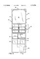
- the apparatus 10 of the present invention is useful for coating a surface of a plate-like material and includes a plurality of treatment modules including thermal conditioning modules 12, a spin coating, or dispense, assembly 14, and a robotic wafer handling assembly 16 for retrieving wafers 18 from a cassette 19 and delivering the wafers 18 to various components according to handling instructions provided by a host controller 20.
- the apparatus 10 is generally rectangularly shaped having a front 22, a back 24, sides 26, a top 28 and a bottom 29.
- a frame 30 is provided having a front portion 32, a middle portion 34 and a back portion 36.
- the frame 30 is sized to support the thermal conditioning modules 12, the spin coating assembly 14 and the robotic wafer handling assembly 16.
- the front and back portions, 32 and 36, respectively, are two directly opposing assemblies having directly opposing faces, 33 and 35, respectively, through which the plate-like material is placed into the treatment modules.
- the front portion 32, or first assembly contains the spin coating assembly 14.
- the back portion 36, or second assembly contains the remaining treatment modules including the thermal conditioning modules 12.
- the back portion 36 also contains a plurality of horizontal shelves 38 conditioning modules 12 from the back 24 of the apparatus 10 and an electronics cabinet 40 containing the host controller 20 is loaded above the shelves 38.
- the middle portion 34 includes a horizontal robot support shelf 42 disposed around the wafer handling assembly 16 between the sides 26 and the front and back portion, 32 and 36, respectively, of the frame 30.
- all equipment and electronics not directly associated with treating the wafers 18 are positioned in the back portion 36 of the frame 30 so as to segregate the components of the apparatus and optimize the amount of equipment and electronics necessary in a clean room 37.
- all of the treatment modules can be fully accessed from the outwardly opposing front and back faces 22 and 24 and from one of the opposing faces 33 and 35 defining the middle portion 34. This allows the apparatuses to be placed in a side-by-side arrangement with the back portion 36 extending outside of the clean room 37 into an external plenum region 39 as shown in FIG. 6, thereby providing maintenance access to the electronics from outside the clean room.
- the top 28 of the apparatus 10 is substantially open to provide access to remove the robotic wafer handling assembly 16 without having to disturb the side-by-side arrangement of the apparatuses.
- the lifting of the robotic wafer handling assembly 16 can be performed using a portable counterbalanced crane assembly having a crane arm that can be extended beyond the base of the crane to lift the assembly or by any conventional method.
- the bottom 29 of the apparatus 10 preferably has a raised portion such that lift bars can be slid beneath the bottom 29 and the apparatus can be lifted and moved using the bars, such as by employing opposing portable wheeled jacks at each end of the lifting bars or by conventional methods.
- the robotic wafer handling assembly 16 includes a horizontally stationary, vertically actuating robot 50 centered in the support shelf 42 having an actuating portion 52 extending above the support shelf 42 and a stationary portion 54 positioned below the support shelf 42.
- the actuating portion 52 includes at least one, preferably two, rotatable reciprocating end effectors, or "arms", 55 that can be reciprocated to insert and remove wafers 18 from the various components and a wafer mapping system (not shown) to scan the cassette 19 with a laser/detector to determine the presence of the wafer 18 and the precise vertical location of the wafer 18.
- a robot controller 58 is slidably disposed through the back 24, rests on horizontal shelves 38 below the plane of the support shelf 42 and is attached to the robot 50.
- an Equipe Technologies, Inc. (Sunnyvale, Calif.) Model No. ATM-307-2-CSX robot is used with an Equipe Technologies controller Part No. ESC-100 ATM and a model DD-50 laser/detector system manufactured by Hama Laboratories (Palo Alto, Calif.).
- any commercially available robots having the general characteristics described herein can be used in the present invention, including robotic handling assemblies 16 that do not contain a dedicated controller, but are controlled by the host controller 20.
- the robotic wafer handling assembly 16 also includes wafer prealigner 60 that is slidably disposed through the back 24 onto the shelving 38 above the support shelf 42 and is used to center the wafer 18 before the wafer 18 is put into the spin coating assembly 14.
- An alignment controller 62 is attached to and controls the prealigner 60 and is connected to and receives alignment instructions from the host controller 20.
- the alignment controller 62 is slidably disposed through the back 24 onto the shelving 38 below the support shelf 42 in the back portion 36.
- a commercially available wafer prealigner 60 such as an Equipe Technologies PRE-201, and alignment controllers 62, such as Equipe Technologies ESC-101, can be used with the present invention.
- the prealigner 60 can be directly controlled from the host controller 20 or the robot controller 58 can be used to control the prealigner 60, in addition to the robot 50.
- thermal conditioning modules 12 including three heating, or bake, modules 70 and three cooling, or chill, modules 72, are slidably disposed through the back 24 on shelves 38 divided into three rows and two columns above the support shelf 42.
- the bake modules are used to preheat the wafer in order to drive off water vapor from the surface before spin coating photoresist material onto the surface of the wafer and also to bake the wafer following the application of the photoresist in order to harden, or cure, the photoresist coating.
- the chill modules 72 are used to cool the wafer 18 to process temperature following preheating and to lower the temperature of the wafer following the baking process.
- the total number of thermal conditioning modules 12, as well as the arrangement in terms of rows and columns, can be optimized by the practitioner depending upon the processing speed of the spin coating assembly 14 and the capabilities of the robotic assembly assembly 16.
- the thermal conditioning modules 12 are preferably self-contained heating and cooling modules, 70 and 72, respectively, that contain individual controllers and can an act as stand alone units, if necessary, as described in the U.S. patent application Ser. No. 08/667,704 entitled "Self-Contained Thermal Conditioning Apparatus", which is incorporated herein by reference. While it is preferred that a self-contained thermal conditioning module is used, other commercially available thermal conditioning modules can be used including thermal conditioning modules 12 that must be controlled by the host controller.
- the spin dispense assembly 14 is positioned in the front portion 32 of the frame 30 in a spin station process enclosure 80 defined by frame 30.
- the enclosure includes a support table 82 on which various components of the spin dispense assembly 14 are seated, a back 84 through which the wafers 18 are loaded using the wafer handling assembly 16, a front door 86 that provides an operator with access to the enclosure 80 and a top 88.
- the enclosure 80 is a semi-isolated environment in that access is limited to a portion of the back 84 through which the wafers 18 are placed into the spin assembly 14.
- An environmental control unit 90 that is external to the apparatus 10 and outside the clean room environment is used to control the air temperature and humidity level within the enclosure to specified process conditions and to provide a continuous air flow through the enclosure 80.
- the process air is plumbed through the back 24 of the apparatus 10 into the enclosure 80 through an air filter 92, such as an ULPA filter manufactured by Filtra Corporation (Hawthorne, N.J.) Part No. 5020493103/4X21, and circulated through the enclosure 80.
- a humidity sensor 94 such as General Precision Inc. (Valencia, Calif.) Part Nos. 90109, 90110, 90125, is also included to monitor and provide feedback control over the conditions of the process air within the enclosure 80.
- the spin assembly 14 includes a process bowl 100 seated on the table 82 and attached to a drain system (not shown) which extends through the support table 82 and is plumbed out through the back 24 or bottom 29 of the apparatus 10.
- a rotatable spindle chuck 102 is disposed within the bowl 100 and is connected by a shaft (not shown) to and rotated by a spindle 104 that is vertically actuated using a spindle lift axis actuator 106 through an opening in the bowl 100 and the support table 82.
- Commercially available bowl, chuck and drain arrangements can be used with the present invention; however it is preferred that bowl and chuck arrangement be used such as that described in the U.S.
- the actuator 106 is positioned in the front portion 32 of the frame 30 beneath enclosure 80 and is preferably a serve controlled linear slide having programmable position control to provide precise control over the movement of the chuck 102.
- an IAI America Inc. (Torrence, Calif.) Part No. 25-M-2-S-10-100-2 can be used in the present invention in conjunction with an actuator controller 109, such as an Intelligent actuator manufactured by IAI America, which is positioned on shelves 38 on the back portion 36 below table 42 and connected to the host controller 20.
- the spin assembly 14 further includes a dispense arm 110 that is movably positioned on the support table 82 to dispense appropriate chemicals onto the wafer 18 positioned on the chuck 102.
- the dispense arm 110 is plumbed out the back 24 of the apparatus 10 to a chemical supply source 112 outside of the clean room which contains the chemicals for use in the spin coating process.
- the chemicals are dispensed onto the wafer 18 from dispense nozzles contained in the dispense arm 110 and the dispense nozzle are stored in a solvent bath 114 between spin coating processes to prevent the chemicals from drying out in the nozzles.
- Three dimensional movement of the dispense arm 110 is preferred to facilitate the proper positioning of the dispense arm 110 to dispense the various chemicals and can be accomplished using commercially available actuating mechanisms for "theta" axis drive 116, "Y” axis drive 118, and "Z” axis drive 120, such as from IAI America Inc. Model Nos. 12RS-80-360050-TS, IS-S-Y-M-8-60-300 and IS-S-X-M-80-60-100, respectively.
- the movement of the dispense arm 110 is also controlled by actuator controller 109.
- the dispense arm 110 provides for temperature control of coating material, such as is described in the U.S. patent application Ser. No.
- a spin station controller 122 is provided to oversee the entire spin coating operation and is located in the electronics cabinet 40. Commercially available controllers can be used as the spin station controller 122, such as a Model 4025A 486 Single Board Computer from Octagon Systems Corp. (Westminster, Conn.).
- the spin station controller 122 interfaces with the spindle controller 108, the actuator controller 109, the environmental system 90, and the chemical supply source 112 and the host controller 20 to coordinate the sequencing and timing of the spin coating operation.
- two cassette loading platforms 126 are positioned on the top 88 of the process enclosure 80 in the front portion 32 of the frame 30.
- the platforms 126 are oriented such that when the cassette 19 containing wafers 18 is placed on the platform 126, the wafers 18 can be removed by the robot arm 55.
- a cassette sensor 128 is used to detect the presence of the cassette 19 and to provide a signal to the host controller 20 indicating the presence or absence of the cassette 19. While a current preferred embodiment incorporates two loading platforms 126, the preference is necessarily dictated by the selection of components to be used in any given embodiment of the apparatus 10.
- additional platforms could be provided above the two platforms, requiring only that the robot assembly 16 be capable of reciprocating to a level where the wafers 18 can be removed from the cassette 19.
- the additional capacity described does not require that the footprint of the apparatus 10 be increased, because the footprint is governed only by the desired capacity of the processing equipment used in the apparatus 10 and not the wafer load/unload requirements as in the prior art.
- the display 130 is preferably a flatpanel touchscreen display, such as manufactured by Dolch Computer (Fremont, Calif.). It is also preferred that a similar host input/output display device be remotely attachable to the back 24 (not shown) of the apparatus 10 to allow the operator to monitor the apparatus 10 from outside the clean room.
- the host controller 20 is also preferably connected to a network including user access locations 132, which provides oversight and control access to production personnel, a database or recipe server 134, and a support equipment management server 136 that controls the environmental control system 90 and the chemical supply source 112, in addition to coating material temperature controllers and pumps 137 and 138, respectively. Because there is no need for this equipment to be in the clean room, all of the above operations are controlled and performed externally to the clean room and the process chemicals and system air are plumbed to the apparatus 10. Alternatively, the information contained in the recipe server 134 can be stored in memory attached to the host controller 20.
- the wafers 18 in the cassette 19 are identified using a bar code.
- the bar codes are scanned, or read, by a bar code reader (not shown), such as a Symbol Technologies Inc. (Bohemia, N.Y.) Model LS-3000-1000A, and the scanned information is passed to the host controller 20, which accesses the processing instructions, or "recipe", for those particular wafers 18 from the system database 134.
- the processing instructions provide the details of the particular process to be performed on the wafers 18 in terms of a specific sequence of handling instructions and treatment instructions to be sent to the handling device and treatment modules by the host controller 20.
- such treatment information includes the coating materials to be applied, the solvents to be used, the temperature, amounts and dispense rates of the coating materials and solvents, the heating and cooling temperatures and rates for the wafers, the wafer spin rates and times, the system temperature and exhaust air flow, etc.
- the operator loads the cassette 19 containing wafers 18 to be processed onto the cassette platform 126.
- the cassette sensor 128 detects the presence of the cassette 19 and provides a signal to the host controller 20 indicating the presence of the cassette 19.
- the operator scans the bar code associated with the wafers using the bar code reader and the scanned code is transmitted to the host controller 20.
- the host controller 20 queries the system database 132 using the code to obtain the processing instructions for the wafers 18 corresponding to the code.
- the host controller 20 After receiving the handling and treatment instructions, or recipe, the host controller 20 transmits to the support equipment manager server 136 instructions regarding 1) the chemicals to be used in the process, 2) the temperature of the chemicals, 3) the flow rate of the chemicals, and 4) the system air temperature and exhaust flow rate.
- the support equipment manager server 136 takes this information and distributes it to the chemical supply source 112, the fluid temperature controllers 137, the chemical pumps 138 and the environmental control system 90, respectively.
- the support equipment manager server 136 monitors the status of the chemical and environmental systems for compliance with the process instructions and queues the host controller 20 when the process conditions have been attained prior to processing and if attainment of the processing conditions is lost during processing.
- the host controller 20 sends a signal to the robot controller 58 to scan the cassette 19 for wafers 18.
- the robot controller 58 activates the robot 50 to align the laser to be radially pointing toward the center of the wafer 18 and slightly below the level of the wafer 18.
- the robot controller 58 activates the laser and actuates the actuating portion 52 of the robot 50 vertically past the cassette 19 to record the vertical location of the wafers 18 in the cassette. This information is compared to the vertical location of the slots in the cassette stored in the robot controller 58 to determine which slots contain wafers 18.
- the host controller then directs the robot controller 58 to remove the first wafer 18 from the cassette 19 and place the wafer 18 in the treatment module called for in the recipe.
- the robot controller 58 then directs the robot 50 to move the actuating portion 52 to the precise level provided by the mapping system and then for the robot 50 to reciprocate arm 55 to reach into the cassette 19 and remove the wafer.
- the host controller 20 sends handling instructions to the robot controller 58 indicating the location of the first treatment module in which the wafer is to be processed. If, for example, the first processing step is a preheating step to drive moisture from the surface of the wafer, the host controller 20 also sends thermal conditioning instructions signal to heating module 70 providing the temperature and rate and duration of heating for processing the wafer.
- the robot 50 is directed by the robot controller 58 to move the wafer from the cassette 19 to the heating module 70.
- the robot controller 58 informs the host controller 20 and the host controller 20 directs the heating module 70 to perform the preheating operations using the operating instructions supplied by the host controller 20.
- the heating module 70 can be provided with a sensor to detect the presence of the wafer before executing the heating instructions provided by the host controller 20. While the preheating operations are taking place, the robot 50 can be directed by the host controller 20 via the robot controller 58 to perform other operations.
- the host controller 20 provides handling instructions to the robot controller 58 to remove the wafer from the location of the heating module 70 and move the wafer a location in the cooling module 72.
- the cooling module 72 detects the presence of the wafer, the cooling module 72 performs the cooling operations using the thermal conditioning instructions supplied by the host controller 20.
- the host controller 20 sends handling instructions to the robot controller 58 to remove the wafer from the cooling module 72 and move the wafer into the wafer prealigner 60 and also sends alignment instructions to the alignment controller 62, which in turn controls the prealigner during the alignment of the wafer. Following the alignment, the host controller 20 signal the robot 50 to remove the wafer from the prealigner. The host controller 20 sends the instructions to the spin station controller 122 to process the wafer 18 according to the recipe supplied by the host controller 20.
- the environmental control system 90 monitors the temperature and humidity conditions in the process enclosure 80 and signals the host controller 20 if the system operating conditions fall out of specification. If the operating conditions are in specification, the spin station controller 122 runs the recipe by coordinating instructions to the spindle controller 108, the actuator controller 109, environmental system 90 and input/output with the host controller 20 according to the timing and sequencing call for in the recipe.
- the spin station controller 122 will instruct the spindle controller 108 to begin spinning the spindle and to move dispense arm 110 from a stored position in the solvent bath 114 to a dispense position above the wafer in the process bowl 100 and the actuator controller 122 directs the theta, Y and Z drives, 116, 118, and 120, respectively, to perform the movement.
- the spin station controller 122 directs the support equipment management server 136 to operate the chemical pumps and 138 to deliver a prescribed amount of coating material at a prescribed rate through the dispense arm 110 to the wafer 18.
- the spin station controller 122 directs the actuator controller 109 to return the dispense arm 110 to the solvent bath 114 and directs the spindle controller 108 to stop the spinning of the chuck 102.
- the spin station controller 122 instructs the actuator controller 109 to lift the chuck 102 to the loading position, after which the environmental control system is instructed to release the vacuum.
- spin station controller 122 instructs the host controller 20 that the process is completed.
- the host controller 20 instructs the robot controller 58 to move the robot 50 into position and remove the wafer from the chuck 102.
- the host controller 20 directs the robot controller 58 to move the wafer into the heating module 70 and sends the heating module 70 thermal conditioning instructions providing the temperature and heating rate and duration of the heat treatment.
- the host controller 20 Upon completion of the heating of the wafer, the host controller 20 prompts the robot controller 58 to remove the wafer from the heating module and place the wafer into the cooling module 72.
- the host controller 20 provides temperature and cooling rate and duration instructions, to the cooling module 72, after which the robot controller 58 is prompted to remove the wafer from the cooling module 72 and place the wafer back into the cassette 19.
- the number of wafers that can be processed during a given time period by the apparatus is invariably dependent upon the duration of the processing times of the various steps called for by the specific recipe.
- the present invention provides an apparatus that has the flexibility to allow the processing of wafers to be performed in any sequence and without limitations as to the steps that must be included.
- the apparatus 10 embodies a higher architectural control level that allows the present invention to employ an integrated structure of autonomous distinct components, which greatly simplifies system analysis, testing and calibration and system layout.
- the high level of control allows the flexibility of the system to be exploited using relatively straightforward processing algorithms or recipes.
- a further benefit of the modular apparatus is realized in a preferred system layout which provides access to all treatment modules from the front and back of the apparatus, thereby allowing the apparatuses to be closely packed in a clean room environment.
- the placement of the treatment modules, excluding the coating assembly, on one side of the apparatus allow a portion of the apparatus to be outside of the clean room, further reducing the size of the clean room, and also allowing the treatment modules to be maintained from outside the clean room, further reducing maintenance downtime. While one embodiment of the present invention has been described incorporating distinct control structures for all of the system components, the present invention can be effectively employed for use with systems in which completely distinct hierarchical control may not be necessary or desirable. In those cases, the host controller, in addition to providing high level control of those components incorporating individual controllers, would provide lower level direct control of other operations.
- the present invention provides significant advantages over the prior art for process liquid dispense systems.
- the subject invention provides a more compacted apparatus for use in a clean room environment.
- the invention minimizes downtime for maintenance by providing stand alone component modules that can be maintained and replaced from outside the clean room and without extended shutdown for calibration. While the subject invention provides these and other advantages over other the prior art, it will be understood, however, that various changes in the details, materials and arrangements of parts which have been herein described and illustrated in order to explain the nature of the invention may be made by those skilled in the art within the principle and scope of the invention as expressed in the appended claims.
Abstract
Description
Claims (18)
Priority Applications (4)
| Application Number | Priority Date | Filing Date | Title |
|---|---|---|---|
| US08/667,738 US5779799A (en) | 1996-06-21 | 1996-06-21 | Substrate coating apparatus |
| US08/951,176 US6061605A (en) | 1996-06-21 | 1997-10-15 | Methods of treating a semiconductor wafer |
| US09/114,449 US6113694A (en) | 1996-06-21 | 1998-07-13 | Substrate treatment apparatus |
| US09/562,108 US6477440B1 (en) | 1996-06-21 | 2000-05-01 | Methods of treating a semiconductor wafer |
Applications Claiming Priority (1)
| Application Number | Priority Date | Filing Date | Title |
|---|---|---|---|
| US08/667,738 US5779799A (en) | 1996-06-21 | 1996-06-21 | Substrate coating apparatus |
Related Child Applications (2)
| Application Number | Title | Priority Date | Filing Date |
|---|---|---|---|
| US08/951,176 Division US6061605A (en) | 1996-06-21 | 1997-10-15 | Methods of treating a semiconductor wafer |
| US09/114,449 Continuation US6113694A (en) | 1996-06-21 | 1998-07-13 | Substrate treatment apparatus |
Publications (1)
| Publication Number | Publication Date |
|---|---|
| US5779799A true US5779799A (en) | 1998-07-14 |
Family
ID=24679429
Family Applications (4)
| Application Number | Title | Priority Date | Filing Date |
|---|---|---|---|
| US08/667,738 Expired - Lifetime US5779799A (en) | 1996-06-21 | 1996-06-21 | Substrate coating apparatus |
| US08/951,176 Expired - Lifetime US6061605A (en) | 1996-06-21 | 1997-10-15 | Methods of treating a semiconductor wafer |
| US09/114,449 Expired - Lifetime US6113694A (en) | 1996-06-21 | 1998-07-13 | Substrate treatment apparatus |
| US09/562,108 Expired - Fee Related US6477440B1 (en) | 1996-06-21 | 2000-05-01 | Methods of treating a semiconductor wafer |
Family Applications After (3)
| Application Number | Title | Priority Date | Filing Date |
|---|---|---|---|
| US08/951,176 Expired - Lifetime US6061605A (en) | 1996-06-21 | 1997-10-15 | Methods of treating a semiconductor wafer |
| US09/114,449 Expired - Lifetime US6113694A (en) | 1996-06-21 | 1998-07-13 | Substrate treatment apparatus |
| US09/562,108 Expired - Fee Related US6477440B1 (en) | 1996-06-21 | 2000-05-01 | Methods of treating a semiconductor wafer |
Country Status (1)
| Country | Link |
|---|---|
| US (4) | US5779799A (en) |
Cited By (63)
| Publication number | Priority date | Publication date | Assignee | Title |
|---|---|---|---|---|
| US5958517A (en) * | 1996-12-19 | 1999-09-28 | Texas Instruments Incorporated | System and method for cleaning nozzle delivering spin-on-glass to substrate |
| US5972110A (en) * | 1996-09-06 | 1999-10-26 | Tokyo Electron Limited | Resist processing system |
| US5989945A (en) * | 1996-05-15 | 1999-11-23 | Seiko Epson Corporation | Thin film device provided with coating film, liquid crystal panel and electronic device, and method for making the thin film device |
| US6000830A (en) * | 1997-04-18 | 1999-12-14 | Tokyo Electron Limited | System for applying recipe of semiconductor manufacturing apparatus |
| US6071055A (en) * | 1997-09-30 | 2000-06-06 | Applied Materials, Inc. | Front end vacuum processing environment |
| US6113694A (en) * | 1996-06-21 | 2000-09-05 | Micron Technology, Inc. | Substrate treatment apparatus |
| US6319322B1 (en) * | 1998-07-13 | 2001-11-20 | Tokyo Electron Limited | Substrate processing apparatus |
| US20020022363A1 (en) * | 1998-02-04 | 2002-02-21 | Thomas L. Ritzdorf | Method for filling recessed micro-structures with metallization in the production of a microelectronic device |
| US6350316B1 (en) * | 1998-11-04 | 2002-02-26 | Tokyo Electron Limited | Apparatus for forming coating film |
| US6364745B1 (en) * | 1997-09-10 | 2002-04-02 | Speedfam-Ipec Corporation | Mapping system for semiconductor wafer cassettes |
| US6371713B1 (en) * | 1997-09-01 | 2002-04-16 | Dainippon Screen Mfg. Co., Ltd. | Substrate processing apparatus |
| US20020075422A1 (en) * | 1996-09-19 | 2002-06-20 | Seiko Epson Corporation | Matrix type display device and manufacturing method thereof |
| US20020074233A1 (en) * | 1998-02-04 | 2002-06-20 | Semitool, Inc. | Method and apparatus for low temperature annealing of metallization micro-structures in the production of a microelectronic device |
| US6420864B1 (en) | 2000-04-13 | 2002-07-16 | Nanophotonics Ag | Modular substrate measurement system |
| US6432204B1 (en) * | 2000-05-17 | 2002-08-13 | Tokyo Electron Limited | Temperature and humidity controlled processing system |
| US20020136823A1 (en) * | 1996-11-25 | 2002-09-26 | Seiko Epson Corporation | Method of manufacturing organic EL element, organic EL element, and organic EL display device |
| US20020137346A1 (en) * | 2001-03-12 | 2002-09-26 | Applied Materials. Inc. | Workpiece distribution and processing in a high throughput stacked frame |
| US6523563B2 (en) * | 2000-02-28 | 2003-02-25 | Applied Materials, Inc. | Modular gas panel closet for a semiconductor wafer processing platform |
| US6548115B1 (en) * | 1998-11-30 | 2003-04-15 | Fastar, Ltd. | System and method for providing coating of substrates |
| US20030215357A1 (en) * | 2002-05-13 | 2003-11-20 | Nigel Malterer | Automated processing system and method of using same |
| US20040007799A1 (en) * | 2002-07-11 | 2004-01-15 | Choi Byung Jin | Formation of discontinuous films during an imprint lithography process |
| US6687562B2 (en) * | 2000-02-16 | 2004-02-03 | Cymer, Inc. | Process monitoring system for lithography lasers |
| US6697695B1 (en) * | 2000-04-25 | 2004-02-24 | Komatsu Ltd. | Laser device management system |
| US6696220B2 (en) | 2000-10-12 | 2004-02-24 | Board Of Regents, The University Of Texas System | Template for room temperature, low pressure micro-and nano-imprint lithography |
| US20040052618A1 (en) * | 2002-09-12 | 2004-03-18 | Hitachi Kokusai Electric Inc. | Semiconductor device producing apparatus and producing method of semiconductor device |
| US20040052956A1 (en) * | 1995-07-27 | 2004-03-18 | Courtenay Robert William | Method and apparatus for coating a wafer |
| US6719915B2 (en) | 1999-03-11 | 2004-04-13 | Board Of Regents, The University Of Texas System | Step and flash imprint lithography |
| US20040081756A1 (en) * | 2001-12-03 | 2004-04-29 | Coots Timothy D. | Workpiece coating apparatus |
| US20040154535A1 (en) * | 2002-10-18 | 2004-08-12 | Applied Materials, Inc. | Modular electrochemical processing system |
| US20040186609A1 (en) * | 2000-02-16 | 2004-09-23 | Patel Parthiv S. | Process monitoring system for lithography lasers |
| US6821550B2 (en) * | 1998-06-05 | 2004-11-23 | Tokyo Electron Limited | Apparatus and method for applying process solution |
| US6873087B1 (en) | 1999-10-29 | 2005-03-29 | Board Of Regents, The University Of Texas System | High precision orientation alignment and gap control stages for imprint lithography processes |
| US20050156353A1 (en) * | 2004-01-15 | 2005-07-21 | Watts Michael P. | Method to improve the flow rate of imprinting material |
| US6990870B2 (en) | 2002-12-12 | 2006-01-31 | Molecular Imprints, Inc. | System for determining characteristics of substrates employing fluid geometries |
| US20060210704A1 (en) * | 1996-09-19 | 2006-09-21 | Seiko Epson Corporation | Method of manufacturing a display device |
| US20070051306A1 (en) * | 2002-11-19 | 2007-03-08 | Ivanov Igor C | Spatially-arranged chemical processing station |
| US20070059130A1 (en) * | 2005-08-18 | 2007-03-15 | Flitsch Frederick A | Method and apparatus to support a cleanspace fabricator |
| US20070269296A1 (en) * | 2005-09-18 | 2007-11-22 | Flitsch Frederick A | Methods and apparatus for vertically orienting substrate processing tools in a clean space |
| US20080097065A1 (en) * | 2004-02-27 | 2008-04-24 | Molecular Imprints, Inc. | Composition for an etching mask comprising a silicon-containing material |
| US7670530B2 (en) | 2006-01-20 | 2010-03-02 | Molecular Imprints, Inc. | Patterning substrates employing multiple chucks |
| US7670529B2 (en) | 2005-12-08 | 2010-03-02 | Molecular Imprints, Inc. | Method and system for double-sided patterning of substrates |
| US20100209226A1 (en) * | 2005-06-18 | 2010-08-19 | Flitsch Frederick A | Method and apparatus to support process tool modules in a cleanspace fabricator |
| US7803308B2 (en) | 2005-12-01 | 2010-09-28 | Molecular Imprints, Inc. | Technique for separating a mold from solidified imprinting material |
| US20110108124A1 (en) * | 2009-11-12 | 2011-05-12 | Bonner Michael R | Viscosity Feedback Temperature Control System |
| US8016277B2 (en) | 2000-08-21 | 2011-09-13 | Board Of Regents, The University Of Texas System | Flexure based macro motion translation stage |
| US8076386B2 (en) | 2004-02-23 | 2011-12-13 | Molecular Imprints, Inc. | Materials for imprint lithography |
| US8349241B2 (en) | 2002-10-04 | 2013-01-08 | Molecular Imprints, Inc. | Method to arrange features on a substrate to replicate features having minimal dimensional variability |
| US8485392B1 (en) * | 2008-10-08 | 2013-07-16 | Jeffrey Wilson Tarter | System for dispensing solvents |
| US20140011323A1 (en) * | 2012-07-06 | 2014-01-09 | Frederick Flitsch | Processes relating to cleanspace fabricators |
| US8850980B2 (en) | 2006-04-03 | 2014-10-07 | Canon Nanotechnologies, Inc. | Tessellated patterns in imprint lithography |
| TWI456684B (en) * | 2011-06-29 | 2014-10-11 | Grand Plastic Technology Co Ltd | An apparatus of wet processor with wafer cassette automatically transfering from a spin dryer |
| US20140312070A1 (en) * | 2003-10-31 | 2014-10-23 | Nordson Corporation | Hot Melt Adhesive System And Method Using Machine Readable Information |
| US9034425B2 (en) | 2012-04-11 | 2015-05-19 | Nordson Corporation | Method and apparatus for applying adhesive on an elastic strand in a personal disposable hygiene product |
| US9059227B2 (en) | 2005-06-18 | 2015-06-16 | Futrfab, Inc. | Methods and apparatus for vertically orienting substrate processing tools in a clean space |
| US9159592B2 (en) | 2005-06-18 | 2015-10-13 | Futrfab, Inc. | Method and apparatus for an automated tool handling system for a multilevel cleanspace fabricator |
| US9168554B2 (en) | 2011-04-11 | 2015-10-27 | Nordson Corporation | System, nozzle, and method for coating elastic strands |
| US9223202B2 (en) | 2000-07-17 | 2015-12-29 | Board Of Regents, The University Of Texas System | Method of automatic fluid dispensing for imprint lithography processes |
| CN103801829B (en) * | 2006-05-11 | 2016-08-17 | 通快激光与系统工程有限公司 | The decentralized control method of machining tool, especially laser process machine |
| US9682392B2 (en) | 2012-04-11 | 2017-06-20 | Nordson Corporation | Method for applying varying amounts or types of adhesive on an elastic strand |
| US9793146B2 (en) | 2005-06-18 | 2017-10-17 | Futrfab, Inc. | Method of forming a cleanspace fabricator |
| US10627809B2 (en) | 2005-06-18 | 2020-04-21 | Frederick A. Flitsch | Multilevel fabricators |
| US10651063B2 (en) | 2005-06-18 | 2020-05-12 | Frederick A. Flitsch | Methods of prototyping and manufacturing with cleanspace fabricators |
| US11024527B2 (en) | 2005-06-18 | 2021-06-01 | Frederick A. Flitsch | Methods and apparatus for novel fabricators with Cleanspace |
Families Citing this family (24)
| Publication number | Priority date | Publication date | Assignee | Title |
|---|---|---|---|---|
| JP3784110B2 (en) * | 1996-07-30 | 2006-06-07 | 東京エレクトロン株式会社 | Processing equipment |
| US5824375A (en) * | 1996-10-24 | 1998-10-20 | Applied Materials, Inc. | Decontamination of a plasma reactor using a plasma after a chamber clean |
| WO1999041434A2 (en) * | 1998-02-12 | 1999-08-19 | Acm Research, Inc. | Plating apparatus and method |
| JP3487774B2 (en) * | 1998-11-19 | 2004-01-19 | 沖電気工業株式会社 | Transport method in semiconductor device manufacturing process |
| JP3926940B2 (en) * | 1998-12-17 | 2007-06-06 | 株式会社小糸製作所 | Lens surface treatment method for vehicular lamp |
| US6656273B1 (en) * | 1999-06-16 | 2003-12-02 | Tokyo Electron Limited | Film forming method and film forming system |
| JP3730810B2 (en) * | 1999-07-09 | 2006-01-05 | 東京エレクトロン株式会社 | Container moving apparatus and method |
| US6577914B1 (en) * | 1999-08-10 | 2003-06-10 | Advanced Micro Devices, Inc. | Method and apparatus for dynamic model building based on machine disturbances for run-to-run control of semiconductor devices |
| US6662225B1 (en) * | 1999-11-16 | 2003-12-09 | Ricoh Company, Ltd. | Remote system usage monitoring with flexible packaging of data |
| JP3590328B2 (en) * | 2000-05-11 | 2004-11-17 | 東京エレクトロン株式会社 | Coating and developing method and coating and developing system |
| US6549822B1 (en) * | 2000-07-25 | 2003-04-15 | Advanced Micro Devices, Inc. | Method and apparatus for control of multi-cup semiconductor manufacturing tracks |
| US20020045967A1 (en) * | 2000-10-17 | 2002-04-18 | Masayuki Nakano | Substrate processing system |
| US7153364B1 (en) | 2000-10-23 | 2006-12-26 | Advance Micro Devices, Inc. | Re-circulation and reuse of dummy-dispensed resist |
| US6560506B2 (en) * | 2000-12-04 | 2003-05-06 | Advanced Micro Devices, Inc. | Method and apparatus for control for semiconductor processing for reducing effects of environmental effects |
| US7100826B1 (en) * | 2001-03-26 | 2006-09-05 | Advanced Micro Devices, Inc. | Barcode marking of wafer products for inventory control |
| TW544797B (en) * | 2001-04-17 | 2003-08-01 | Kobe Steel Ltd | High-pressure processing apparatus |
| US6573522B2 (en) | 2001-06-27 | 2003-06-03 | Applied Matrials, Inc. | Locator pin integrated with sensor for detecting semiconductor substrate carrier |
| US20030125821A1 (en) * | 2001-10-01 | 2003-07-03 | Trotter Victor D. | Modular process platform |
| TW518731B (en) * | 2001-10-19 | 2003-01-21 | Ritdisplay Corp | Mass production package apparatus and method for organic electroluminescent display device |
| DE20205819U1 (en) * | 2002-04-12 | 2003-08-21 | Kinetics Germany Gmbh | Device for providing high-purity process chemicals |
| KR100486690B1 (en) * | 2002-11-29 | 2005-05-03 | 삼성전자주식회사 | Substrate processing apparatus and method for controlling contamination in substrate transfer module |
| US6954711B2 (en) * | 2003-05-19 | 2005-10-11 | Applied Materials, Inc. | Test substrate reclamation method and apparatus |
| US7462011B2 (en) * | 2004-08-12 | 2008-12-09 | Tokyo Electron Limited | Substrate processing system, substrate processing method, sealed container storing apparatus, program for implementing the substrate processing method, and storage medium storing the program |
| JP6114708B2 (en) * | 2013-05-27 | 2017-04-12 | 東京エレクトロン株式会社 | Substrate desorption detection apparatus and substrate desorption detection method, and substrate processing apparatus and substrate processing method using the same |
Citations (13)
| Publication number | Priority date | Publication date | Assignee | Title |
|---|---|---|---|---|
| US4985722A (en) * | 1988-02-12 | 1991-01-15 | Tokyo Electron Limited | Apparatus for coating a photo-resist film and/or developing it after being exposed |
| US5177514A (en) * | 1988-02-12 | 1993-01-05 | Tokyo Electron Limited | Apparatus for coating a photo-resist film and/or developing it after being exposed |
| US5202716A (en) * | 1988-02-12 | 1993-04-13 | Tokyo Electron Limited | Resist process system |
| US5403397A (en) * | 1992-10-21 | 1995-04-04 | Od & Me B.V. | Device for manufacturing a mold for a disc-shaped registration carrier |
| US5405443A (en) * | 1992-04-24 | 1995-04-11 | Tokyo Electron Limited | Substrates processing device |
| US5429912A (en) * | 1993-08-02 | 1995-07-04 | Chartered Semiconductor Manufacturing Pte Ltd. | Method of dispensing fluid onto a wafer |
| US5510724A (en) * | 1993-05-31 | 1996-04-23 | Tokyo Electron Limited | Probe apparatus and burn-in apparatus |
| US5516732A (en) * | 1992-12-04 | 1996-05-14 | Sony Corporation | Wafer processing machine vacuum front end method and apparatus |
| US5518542A (en) * | 1993-11-05 | 1996-05-21 | Tokyo Electron Limited | Double-sided substrate cleaning apparatus |
| US5536128A (en) * | 1988-10-21 | 1996-07-16 | Hitachi, Ltd. | Method and apparatus for carrying a variety of products |
| US5555177A (en) * | 1994-05-27 | 1996-09-10 | Ontrak Systems, Inc. | Method and apparatus for resetting individual processes in a control system |
| US5565034A (en) * | 1993-10-29 | 1996-10-15 | Tokyo Electron Limited | Apparatus for processing substrates having a film formed on a surface of the substrate |
| US5578127A (en) * | 1993-02-08 | 1996-11-26 | Tokyo Electron Ltd | System for applying process liquid |
Family Cites Families (8)
| Publication number | Priority date | Publication date | Assignee | Title |
|---|---|---|---|---|
| JPH0616475B2 (en) * | 1987-04-03 | 1994-03-02 | 三菱電機株式会社 | Article manufacturing system and article manufacturing method |
| US5255197A (en) * | 1990-07-06 | 1993-10-19 | Honda Giken Kogyo Kabushiki Kaisha | Line production management system |
| JP2644912B2 (en) * | 1990-08-29 | 1997-08-25 | 株式会社日立製作所 | Vacuum processing apparatus and operating method thereof |
| FR2706016B1 (en) * | 1993-06-03 | 1995-07-28 | France Prod Oxygenes Co | Gas bottle cap. |
| EP0634699A1 (en) * | 1993-07-16 | 1995-01-18 | Semiconductor Systems, Inc. | Clustered photolithography system |
| JP3033009B2 (en) * | 1994-09-09 | 2000-04-17 | 東京エレクトロン株式会社 | Processing equipment |
| JP3732250B2 (en) * | 1995-03-30 | 2006-01-05 | キヤノンアネルバ株式会社 | In-line deposition system |
| US5779799A (en) * | 1996-06-21 | 1998-07-14 | Micron Technology, Inc. | Substrate coating apparatus |
-
1996
- 1996-06-21 US US08/667,738 patent/US5779799A/en not_active Expired - Lifetime
-
1997
- 1997-10-15 US US08/951,176 patent/US6061605A/en not_active Expired - Lifetime
-
1998
- 1998-07-13 US US09/114,449 patent/US6113694A/en not_active Expired - Lifetime
-
2000
- 2000-05-01 US US09/562,108 patent/US6477440B1/en not_active Expired - Fee Related
Patent Citations (14)
| Publication number | Priority date | Publication date | Assignee | Title |
|---|---|---|---|---|
| US5177514A (en) * | 1988-02-12 | 1993-01-05 | Tokyo Electron Limited | Apparatus for coating a photo-resist film and/or developing it after being exposed |
| US5202716A (en) * | 1988-02-12 | 1993-04-13 | Tokyo Electron Limited | Resist process system |
| US5339128A (en) * | 1988-02-12 | 1994-08-16 | Tokyo Electron Limited | Resist processing method |
| US4985722A (en) * | 1988-02-12 | 1991-01-15 | Tokyo Electron Limited | Apparatus for coating a photo-resist film and/or developing it after being exposed |
| US5536128A (en) * | 1988-10-21 | 1996-07-16 | Hitachi, Ltd. | Method and apparatus for carrying a variety of products |
| US5405443A (en) * | 1992-04-24 | 1995-04-11 | Tokyo Electron Limited | Substrates processing device |
| US5403397A (en) * | 1992-10-21 | 1995-04-04 | Od & Me B.V. | Device for manufacturing a mold for a disc-shaped registration carrier |
| US5516732A (en) * | 1992-12-04 | 1996-05-14 | Sony Corporation | Wafer processing machine vacuum front end method and apparatus |
| US5578127A (en) * | 1993-02-08 | 1996-11-26 | Tokyo Electron Ltd | System for applying process liquid |
| US5510724A (en) * | 1993-05-31 | 1996-04-23 | Tokyo Electron Limited | Probe apparatus and burn-in apparatus |
| US5429912A (en) * | 1993-08-02 | 1995-07-04 | Chartered Semiconductor Manufacturing Pte Ltd. | Method of dispensing fluid onto a wafer |
| US5565034A (en) * | 1993-10-29 | 1996-10-15 | Tokyo Electron Limited | Apparatus for processing substrates having a film formed on a surface of the substrate |
| US5518542A (en) * | 1993-11-05 | 1996-05-21 | Tokyo Electron Limited | Double-sided substrate cleaning apparatus |
| US5555177A (en) * | 1994-05-27 | 1996-09-10 | Ontrak Systems, Inc. | Method and apparatus for resetting individual processes in a control system |
Cited By (103)
| Publication number | Priority date | Publication date | Assignee | Title |
|---|---|---|---|---|
| US20060257561A1 (en) * | 1995-07-27 | 2006-11-16 | Micron Technology, Inc. | Method and apparatus for coating a wafer |
| US20040052956A1 (en) * | 1995-07-27 | 2004-03-18 | Courtenay Robert William | Method and apparatus for coating a wafer |
| US20020074547A1 (en) * | 1996-05-15 | 2002-06-20 | Seiko Epson Corporation | Thin film device provided with coating film, liquid crystal panel and electronic device, and method for making the thin film device |
| US5989945A (en) * | 1996-05-15 | 1999-11-23 | Seiko Epson Corporation | Thin film device provided with coating film, liquid crystal panel and electronic device, and method for making the thin film device |
| US7067337B2 (en) | 1996-05-15 | 2006-06-27 | Seiko Epson Corporation | Thin film device provided with coating film, liquid crystal panel and electronic device, and method for making the thin film device |
| US20030134519A1 (en) * | 1996-05-15 | 2003-07-17 | Seiko Epson Corporation | Thin film device provided with coating film, liquid crystal panel and electronic device, and method for making the thin film device |
| US6593591B2 (en) | 1996-05-15 | 2003-07-15 | Seiko Epson Corporation | Thin film device provided with coating film, liquid crystal panel and electronic device, and method the thin film device |
| US7229859B2 (en) | 1996-05-15 | 2007-06-12 | Seiko Epson Corporation | Thin film device provided with coating film, liquid crystal panel and electronic device, and method for making the thin film device |
| US6113694A (en) * | 1996-06-21 | 2000-09-05 | Micron Technology, Inc. | Substrate treatment apparatus |
| US6477440B1 (en) * | 1996-06-21 | 2002-11-05 | Micron Technology, Inc. | Methods of treating a semiconductor wafer |
| US5972110A (en) * | 1996-09-06 | 1999-10-26 | Tokyo Electron Limited | Resist processing system |
| US8431182B2 (en) | 1996-09-19 | 2013-04-30 | Seiko Epson Corporation | Matrix type display device and manufacturing method thereof |
| US20020075422A1 (en) * | 1996-09-19 | 2002-06-20 | Seiko Epson Corporation | Matrix type display device and manufacturing method thereof |
| US8580333B2 (en) | 1996-09-19 | 2013-11-12 | Seiko Epson Corporation | Matrix type display device with optical material at predetermined positions and manufacturing method thereof |
| US20090053396A1 (en) * | 1996-09-19 | 2009-02-26 | Seiko Epson Corporation | Matrix type display device and manufacturing method thereof |
| US20060210704A1 (en) * | 1996-09-19 | 2006-09-21 | Seiko Epson Corporation | Method of manufacturing a display device |
| US20100120185A1 (en) * | 1996-11-25 | 2010-05-13 | Seiko Epson Corporation | Method of manufacturing organic el element, organic el element, and organic el display device |
| US6821553B2 (en) | 1996-11-25 | 2004-11-23 | Seiko Epson Corporation | Method of manufacturing organic EL element, organic EL element, and organic EL display device |
| US20020136823A1 (en) * | 1996-11-25 | 2002-09-26 | Seiko Epson Corporation | Method of manufacturing organic EL element, organic EL element, and organic EL display device |
| US6838192B2 (en) | 1996-11-25 | 2005-01-04 | Seiko Epson Corporation | Method of manufacturing organic EL element, organic EL element, and organic EL display device |
| US20050042477A1 (en) * | 1996-11-25 | 2005-02-24 | Seiko Epson Corporation | Method of manufacturing organic EL element, organic EL element and organic EL display device |
| US8614545B2 (en) | 1996-11-25 | 2013-12-24 | Seiko Epson Corporation | Organic EL display device having a bank formed to fill spaces between pixel electrodes |
| US7662425B2 (en) | 1996-11-25 | 2010-02-16 | Seiko Epson Corporation | Method of manufacturing organic EL element, organic EL element and organic EL display device |
| US6863961B2 (en) | 1996-11-25 | 2005-03-08 | Seiko Epson Corporation | Method of manufacturing organic EL element, organic EL element, and organic EL display device |
| US5958517A (en) * | 1996-12-19 | 1999-09-28 | Texas Instruments Incorporated | System and method for cleaning nozzle delivering spin-on-glass to substrate |
| US6000830A (en) * | 1997-04-18 | 1999-12-14 | Tokyo Electron Limited | System for applying recipe of semiconductor manufacturing apparatus |
| US6896466B2 (en) | 1997-09-01 | 2005-05-24 | Dainippon Screen Mfg. Co, Ltd. | Substrate processing apparatus |
| US6371713B1 (en) * | 1997-09-01 | 2002-04-16 | Dainippon Screen Mfg. Co., Ltd. | Substrate processing apparatus |
| US6364745B1 (en) * | 1997-09-10 | 2002-04-02 | Speedfam-Ipec Corporation | Mapping system for semiconductor wafer cassettes |
| US6071055A (en) * | 1997-09-30 | 2000-06-06 | Applied Materials, Inc. | Front end vacuum processing environment |
| US20020074233A1 (en) * | 1998-02-04 | 2002-06-20 | Semitool, Inc. | Method and apparatus for low temperature annealing of metallization micro-structures in the production of a microelectronic device |
| US7462269B2 (en) | 1998-02-04 | 2008-12-09 | Semitool, Inc. | Method for low temperature annealing of metallization micro-structures in the production of a microelectronic device |
| US6753251B2 (en) | 1998-02-04 | 2004-06-22 | Semitool, Inc. | Method for filling recessed micro-structures with metallization in the production of a microelectronic device |
| US20020022363A1 (en) * | 1998-02-04 | 2002-02-21 | Thomas L. Ritzdorf | Method for filling recessed micro-structures with metallization in the production of a microelectronic device |
| US7244677B2 (en) | 1998-02-04 | 2007-07-17 | Semitool. Inc. | Method for filling recessed micro-structures with metallization in the production of a microelectronic device |
| US6806186B2 (en) | 1998-02-04 | 2004-10-19 | Semitool, Inc. | Submicron metallization using electrochemical deposition |
| US6508920B1 (en) * | 1998-02-04 | 2003-01-21 | Semitool, Inc. | Apparatus for low-temperature annealing of metallization microstructures in the production of a microelectronic device |
| US7001471B2 (en) | 1998-02-04 | 2006-02-21 | Semitool, Inc. | Method and apparatus for low-temperature annealing of metallization microstructures in the production of a microelectronic device |
| US6821550B2 (en) * | 1998-06-05 | 2004-11-23 | Tokyo Electron Limited | Apparatus and method for applying process solution |
| US6319322B1 (en) * | 1998-07-13 | 2001-11-20 | Tokyo Electron Limited | Substrate processing apparatus |
| US6350316B1 (en) * | 1998-11-04 | 2002-02-26 | Tokyo Electron Limited | Apparatus for forming coating film |
| US6548115B1 (en) * | 1998-11-30 | 2003-04-15 | Fastar, Ltd. | System and method for providing coating of substrates |
| US6719915B2 (en) | 1999-03-11 | 2004-04-13 | Board Of Regents, The University Of Texas System | Step and flash imprint lithography |
| US6873087B1 (en) | 1999-10-29 | 2005-03-29 | Board Of Regents, The University Of Texas System | High precision orientation alignment and gap control stages for imprint lithography processes |
| US7203562B2 (en) | 2000-02-16 | 2007-04-10 | Cymer, Inc. | Process monitoring system for lithography lasers |
| US20040186609A1 (en) * | 2000-02-16 | 2004-09-23 | Patel Parthiv S. | Process monitoring system for lithography lasers |
| US6687562B2 (en) * | 2000-02-16 | 2004-02-03 | Cymer, Inc. | Process monitoring system for lithography lasers |
| US6523563B2 (en) * | 2000-02-28 | 2003-02-25 | Applied Materials, Inc. | Modular gas panel closet for a semiconductor wafer processing platform |
| US6420864B1 (en) | 2000-04-13 | 2002-07-16 | Nanophotonics Ag | Modular substrate measurement system |
| US6697695B1 (en) * | 2000-04-25 | 2004-02-24 | Komatsu Ltd. | Laser device management system |
| US6432204B1 (en) * | 2000-05-17 | 2002-08-13 | Tokyo Electron Limited | Temperature and humidity controlled processing system |
| US9223202B2 (en) | 2000-07-17 | 2015-12-29 | Board Of Regents, The University Of Texas System | Method of automatic fluid dispensing for imprint lithography processes |
| US8016277B2 (en) | 2000-08-21 | 2011-09-13 | Board Of Regents, The University Of Texas System | Flexure based macro motion translation stage |
| US6696220B2 (en) | 2000-10-12 | 2004-02-24 | Board Of Regents, The University Of Texas System | Template for room temperature, low pressure micro-and nano-imprint lithography |
| US20020137346A1 (en) * | 2001-03-12 | 2002-09-26 | Applied Materials. Inc. | Workpiece distribution and processing in a high throughput stacked frame |
| US20040081756A1 (en) * | 2001-12-03 | 2004-04-29 | Coots Timothy D. | Workpiece coating apparatus |
| US20030215357A1 (en) * | 2002-05-13 | 2003-11-20 | Nigel Malterer | Automated processing system and method of using same |
| US20040007799A1 (en) * | 2002-07-11 | 2004-01-15 | Choi Byung Jin | Formation of discontinuous films during an imprint lithography process |
| US7198447B2 (en) * | 2002-09-12 | 2007-04-03 | Hitachi Kokusai Electric Inc. | Semiconductor device producing apparatus and producing method of semiconductor device |
| US20040052618A1 (en) * | 2002-09-12 | 2004-03-18 | Hitachi Kokusai Electric Inc. | Semiconductor device producing apparatus and producing method of semiconductor device |
| US8349241B2 (en) | 2002-10-04 | 2013-01-08 | Molecular Imprints, Inc. | Method to arrange features on a substrate to replicate features having minimal dimensional variability |
| US20040154535A1 (en) * | 2002-10-18 | 2004-08-12 | Applied Materials, Inc. | Modular electrochemical processing system |
| US20070051306A1 (en) * | 2002-11-19 | 2007-03-08 | Ivanov Igor C | Spatially-arranged chemical processing station |
| US6990870B2 (en) | 2002-12-12 | 2006-01-31 | Molecular Imprints, Inc. | System for determining characteristics of substrates employing fluid geometries |
| US20140312070A1 (en) * | 2003-10-31 | 2014-10-23 | Nordson Corporation | Hot Melt Adhesive System And Method Using Machine Readable Information |
| US20050156353A1 (en) * | 2004-01-15 | 2005-07-21 | Watts Michael P. | Method to improve the flow rate of imprinting material |
| US8076386B2 (en) | 2004-02-23 | 2011-12-13 | Molecular Imprints, Inc. | Materials for imprint lithography |
| US7906180B2 (en) | 2004-02-27 | 2011-03-15 | Molecular Imprints, Inc. | Composition for an etching mask comprising a silicon-containing material |
| US20080097065A1 (en) * | 2004-02-27 | 2008-04-24 | Molecular Imprints, Inc. | Composition for an etching mask comprising a silicon-containing material |
| US9263309B2 (en) | 2005-06-18 | 2016-02-16 | Futrfab, Inc. | Method and apparatus for an automated tool handling system for a multilevel cleanspace fabricator |
| US11024527B2 (en) | 2005-06-18 | 2021-06-01 | Frederick A. Flitsch | Methods and apparatus for novel fabricators with Cleanspace |
| US9059227B2 (en) | 2005-06-18 | 2015-06-16 | Futrfab, Inc. | Methods and apparatus for vertically orienting substrate processing tools in a clean space |
| US20100209226A1 (en) * | 2005-06-18 | 2010-08-19 | Flitsch Frederick A | Method and apparatus to support process tool modules in a cleanspace fabricator |
| US9159592B2 (en) | 2005-06-18 | 2015-10-13 | Futrfab, Inc. | Method and apparatus for an automated tool handling system for a multilevel cleanspace fabricator |
| US10651063B2 (en) | 2005-06-18 | 2020-05-12 | Frederick A. Flitsch | Methods of prototyping and manufacturing with cleanspace fabricators |
| US10627809B2 (en) | 2005-06-18 | 2020-04-21 | Frederick A. Flitsch | Multilevel fabricators |
| US9793146B2 (en) | 2005-06-18 | 2017-10-17 | Futrfab, Inc. | Method of forming a cleanspace fabricator |
| US9457442B2 (en) * | 2005-06-18 | 2016-10-04 | Futrfab, Inc. | Method and apparatus to support process tool modules in a cleanspace fabricator |
| US20070059130A1 (en) * | 2005-08-18 | 2007-03-15 | Flitsch Frederick A | Method and apparatus to support a cleanspace fabricator |
| US8984744B2 (en) | 2005-08-18 | 2015-03-24 | Futrfab, Inc. | Method and apparatus to support a cleanspace fabricator |
| US9339900B2 (en) | 2005-08-18 | 2016-05-17 | Futrfab, Inc. | Apparatus to support a cleanspace fabricator |
| US8229585B2 (en) * | 2005-09-18 | 2012-07-24 | Flitsch Frederick A | Methods and apparatus for vertically orienting substrate processing tools in a clean space |
| US20070269296A1 (en) * | 2005-09-18 | 2007-11-22 | Flitsch Frederick A | Methods and apparatus for vertically orienting substrate processing tools in a clean space |
| US7803308B2 (en) | 2005-12-01 | 2010-09-28 | Molecular Imprints, Inc. | Technique for separating a mold from solidified imprinting material |
| US7670529B2 (en) | 2005-12-08 | 2010-03-02 | Molecular Imprints, Inc. | Method and system for double-sided patterning of substrates |
| US7670530B2 (en) | 2006-01-20 | 2010-03-02 | Molecular Imprints, Inc. | Patterning substrates employing multiple chucks |
| US8850980B2 (en) | 2006-04-03 | 2014-10-07 | Canon Nanotechnologies, Inc. | Tessellated patterns in imprint lithography |
| CN103801829B (en) * | 2006-05-11 | 2016-08-17 | 通快激光与系统工程有限公司 | The decentralized control method of machining tool, especially laser process machine |
| US8485392B1 (en) * | 2008-10-08 | 2013-07-16 | Jeffrey Wilson Tarter | System for dispensing solvents |
| US9360875B2 (en) * | 2009-11-12 | 2016-06-07 | Michael R. Bonner | Viscosity feedback temperature control system |
| US9904304B2 (en) | 2009-11-12 | 2018-02-27 | Michael R. Bonner | Viscosity feedback temperature control system |
| US20110108124A1 (en) * | 2009-11-12 | 2011-05-12 | Bonner Michael R | Viscosity Feedback Temperature Control System |
| US10046352B2 (en) | 2011-04-11 | 2018-08-14 | Nordson Corporation | System, nozzle and method for coating elastic strands |
| US9168554B2 (en) | 2011-04-11 | 2015-10-27 | Nordson Corporation | System, nozzle, and method for coating elastic strands |
| US10807114B2 (en) | 2011-04-11 | 2020-10-20 | Nordson Corporation | System, nozzle and method for coating elastic strands |
| US10124362B2 (en) | 2011-04-11 | 2018-11-13 | Nordson Corporation | System, nozzle and method for coating elastic strands |
| TWI456684B (en) * | 2011-06-29 | 2014-10-11 | Grand Plastic Technology Co Ltd | An apparatus of wet processor with wafer cassette automatically transfering from a spin dryer |
| US9067394B2 (en) | 2012-04-11 | 2015-06-30 | Nordson Corporation | Method for applying adhesive on an elastic strand in assembly of a personal disposable hygiene product |
| US9962298B2 (en) | 2012-04-11 | 2018-05-08 | Nordson Corporation | Dispensing apparatus for applying adhesive on an elastic strand in a personal disposable hygiene product |
| US9907705B2 (en) | 2012-04-11 | 2018-03-06 | Nordson Corporation | Dispensing apparatus for applying adhesive on an elastic strand in assembly of a personal disposable hygiene product |
| US9682392B2 (en) | 2012-04-11 | 2017-06-20 | Nordson Corporation | Method for applying varying amounts or types of adhesive on an elastic strand |
| US9034425B2 (en) | 2012-04-11 | 2015-05-19 | Nordson Corporation | Method and apparatus for applying adhesive on an elastic strand in a personal disposable hygiene product |
| US20140011323A1 (en) * | 2012-07-06 | 2014-01-09 | Frederick Flitsch | Processes relating to cleanspace fabricators |
Also Published As
| Publication number | Publication date |
|---|---|
| US6113694A (en) | 2000-09-05 |
| US6061605A (en) | 2000-05-09 |
| US6477440B1 (en) | 2002-11-05 |
Similar Documents
| Publication | Publication Date | Title |
|---|---|---|
| US5779799A (en) | Substrate coating apparatus | |
| US7637707B2 (en) | Apparatus for storing and moving a cassette | |
| KR100806418B1 (en) | Substrate processing apparatus | |
| KR100493989B1 (en) | Resist processing system and resist processing method | |
| US20070274711A1 (en) | Substrate processing apparatus and substrate processing method | |
| US8408158B2 (en) | Coating/developing device and method | |
| US20070253710A1 (en) | Method of processing substrate, substrate processing system and substrate processing apparatus | |
| US20070172234A1 (en) | Apparatus for and method of processing substrate | |
| JP4781832B2 (en) | Substrate processing system, substrate processing apparatus, program, and recording medium | |
| US8460476B2 (en) | Apparatus for and method of processing substrate subjected to exposure process | |
| US20120156380A1 (en) | Substrate treating apparatus | |
| US8012418B2 (en) | Apparatus for and method of processing substrate subjected to exposure process | |
| US7364376B2 (en) | Substrate processing apparatus | |
| US20070147832A1 (en) | Method of processing substrate, substrate processing system and substrate processing apparatus | |
| US20050061248A1 (en) | Substrate processing apparatus | |
| US7128481B2 (en) | Substrate processing apparatus for inspecting processing history data | |
| JP4170943B2 (en) | Substrate processing equipment | |
| JP2003218015A (en) | Substrate processing device | |
| JP3460909B2 (en) | Substrate processing system | |
| JPH09275127A (en) | Substrate treatment equipment | |
| JP4255791B2 (en) | Substrate processing equipment | |
| KR101817213B1 (en) | Apparatus for treating substrate | |
| JP4558293B2 (en) | Substrate processing equipment | |
| JP3597285B2 (en) | Substrate processing equipment | |
| JP4323905B2 (en) | Substrate processing equipment |
Legal Events
| Date | Code | Title | Description |
|---|---|---|---|
| AS | Assignment |
Owner name: MICRON TECHNOLOGY, INC., IDAHO Free format text: ASSIGNMENT OF ASSIGNORS INTEREST;ASSIGNOR:DAVIS, SHAWN D.;REEL/FRAME:008073/0125 Effective date: 19960528 |
|
| FEPP | Fee payment procedure |
Free format text: PAYOR NUMBER ASSIGNED (ORIGINAL EVENT CODE: ASPN); ENTITY STATUS OF PATENT OWNER: LARGE ENTITY |
|
| STCF | Information on status: patent grant |
Free format text: PATENTED CASE |
|
| FPAY | Fee payment |
Year of fee payment: 4 |
|
| CC | Certificate of correction | ||
| FPAY | Fee payment |
Year of fee payment: 8 |
|
| FPAY | Fee payment |
Year of fee payment: 12 |
|
| AS | Assignment |
Owner name: U.S. BANK NATIONAL ASSOCIATION, AS COLLATERAL AGENT, CALIFORNIA Free format text: SECURITY INTEREST;ASSIGNOR:MICRON TECHNOLOGY, INC.;REEL/FRAME:038669/0001 Effective date: 20160426 Owner name: U.S. BANK NATIONAL ASSOCIATION, AS COLLATERAL AGEN Free format text: SECURITY INTEREST;ASSIGNOR:MICRON TECHNOLOGY, INC.;REEL/FRAME:038669/0001 Effective date: 20160426 |
|
| AS | Assignment |
Owner name: MORGAN STANLEY SENIOR FUNDING, INC., AS COLLATERAL AGENT, MARYLAND Free format text: PATENT SECURITY AGREEMENT;ASSIGNOR:MICRON TECHNOLOGY, INC.;REEL/FRAME:038954/0001 Effective date: 20160426 Owner name: MORGAN STANLEY SENIOR FUNDING, INC., AS COLLATERAL Free format text: PATENT SECURITY AGREEMENT;ASSIGNOR:MICRON TECHNOLOGY, INC.;REEL/FRAME:038954/0001 Effective date: 20160426 |
|
| AS | Assignment |
Owner name: U.S. BANK NATIONAL ASSOCIATION, AS COLLATERAL AGENT, CALIFORNIA Free format text: CORRECTIVE ASSIGNMENT TO CORRECT THE REPLACE ERRONEOUSLY FILED PATENT #7358718 WITH THE CORRECT PATENT #7358178 PREVIOUSLY RECORDED ON REEL 038669 FRAME 0001. ASSIGNOR(S) HEREBY CONFIRMS THE SECURITY INTEREST;ASSIGNOR:MICRON TECHNOLOGY, INC.;REEL/FRAME:043079/0001 Effective date: 20160426 Owner name: U.S. BANK NATIONAL ASSOCIATION, AS COLLATERAL AGEN Free format text: CORRECTIVE ASSIGNMENT TO CORRECT THE REPLACE ERRONEOUSLY FILED PATENT #7358718 WITH THE CORRECT PATENT #7358178 PREVIOUSLY RECORDED ON REEL 038669 FRAME 0001. ASSIGNOR(S) HEREBY CONFIRMS THE SECURITY INTEREST;ASSIGNOR:MICRON TECHNOLOGY, INC.;REEL/FRAME:043079/0001 Effective date: 20160426 |
|
| AS | Assignment |
Owner name: MICRON TECHNOLOGY, INC., IDAHO Free format text: RELEASE BY SECURED PARTY;ASSIGNOR:U.S. BANK NATIONAL ASSOCIATION, AS COLLATERAL AGENT;REEL/FRAME:047243/0001 Effective date: 20180629 |
|
| AS | Assignment |
Owner name: MICRON TECHNOLOGY, INC., IDAHO Free format text: RELEASE BY SECURED PARTY;ASSIGNOR:MORGAN STANLEY SENIOR FUNDING, INC., AS COLLATERAL AGENT;REEL/FRAME:050937/0001 Effective date: 20190731 |