US5801850A - Linear sensor having a plurality of sensor rows - Google Patents

Linear sensor having a plurality of sensor rows Download PDF

Info

Publication number
US5801850A
US5801850A US08/677,471 US67747196A US5801850A US 5801850 A US5801850 A US 5801850A US 67747196 A US67747196 A US 67747196A US 5801850 A US5801850 A US 5801850A
Authority
US
United States
Prior art keywords
sensor
rows
row
signal
charge
Prior art date
Legal status (The legal status is an assumption and is not a legal conclusion. Google has not performed a legal analysis and makes no representation as to the accuracy of the status listed.)
Expired - Lifetime
Application number
US08/677,471
Inventor
Yasuhito Maki
Motoaki Abe
Tadakuni Narabu
Hideo Nomura
Current Assignee (The listed assignees may be inaccurate. Google has not performed a legal analysis and makes no representation or warranty as to the accuracy of the list.)
Sony Corp
Original Assignee
Sony Corp
Priority date (The priority date is an assumption and is not a legal conclusion. Google has not performed a legal analysis and makes no representation as to the accuracy of the date listed.)
Filing date
Publication date
Priority claimed from JP4093386A external-priority patent/JPH05268524A/en
Priority claimed from JP4093387A external-priority patent/JP3064657B2/en
Application filed by Sony Corp filed Critical Sony Corp
Priority to US08/677,471 priority Critical patent/US5801850A/en
Application granted granted Critical
Publication of US5801850A publication Critical patent/US5801850A/en
Anticipated expiration legal-status Critical
Expired - Lifetime legal-status Critical Current

Links

Images

Classifications

    • HELECTRICITY
    • H04ELECTRIC COMMUNICATION TECHNIQUE
    • H04NPICTORIAL COMMUNICATION, e.g. TELEVISION
    • H04N25/00Circuitry of solid-state image sensors [SSIS]; Control thereof
    • H04N25/70SSIS architectures; Circuits associated therewith
    • H04N25/701Line sensors

Definitions

  • the present invention relates to a solid-state imaging device.
  • it relates to a linear sensor which has a plurality of sensor rows.
  • a linear sensor which has a plurality of rows, for example, three rows formed on a chip is known.
  • the linear sensor is used in an image information input unit such as a color image scanner or a digital color copying machine.
  • the output signals from the rows should be output from one place because the signal processing system can be simplified as compared with the case in which the output signals from the rows are output from three places.
  • FIG. 1 shows a conventional linear sensor.
  • the conventional linear sensor includes three rows 1 1 to 1 3 which are arranged in the vertical direction (V-direction). Each of the sensor rows has a predetermined number of pixels one-dimensionally arranged in the horizontal direction (H-direction).
  • Analog shift registers (hereinafter, called the HCCDs) 2 1 to 2 3 are formed of CCDs (Charge Coupled Devices) for transferring signal charges in the H-direction.
  • Shift gates 3 1 to 3 3 are formed for shifting the signal charges accumulated in the pixels of the sensor rows 1 1 to 1 3 to the HCCDs 2 1 to 2 3 .
  • the signal charges transferred by the HCCDs 2 1 to 2 3 are converted (or reset) into a voltage by, for example, charge/voltage converter units 5 1 to 5 3 of a floating diffusion amplifier provided at the output of the HCCDs 2 1 to 2 3 .
  • Switches SW1 to SW3 are provided at the output sides of the charge/voltage converter units 5 1 to 5 3 . These switches SW1 to SW3 are controlled to be sequentially changed in their positions, so that the signals are output from the rows in order.
  • FIG. 2 shows a timing chart of two different-phase horizontal clocks ⁇ 1, ⁇ 2, read-out pulses ⁇ rog1 to ⁇ rog3 for shift gates 3 1 to 3 3 and an output signal Vout, which are indicated in FIG. 1.
  • the period t int is the signal charge accumulating time for each row.
  • the switches SW1 to SW3 must provided at the output sides of the HCCDs 2 1 to 2 3 and to switch the output signals from the rows. Therefore, when the output signals are to be continuously read, it is necessary to shift the sampling times for the optical signals on the rows.
  • the image information on the three rows cannot be two-dimensionally sampled at substantially a same time.
  • FIG. 3 shows another conventional linear sensor. As shown this figure, several to several tens of pixels of each row are shaded to be optical black (OPB). The outputs from the OPB pixels are used to clamp for the black level correction.
  • OPB optical black
  • FIG. 4 shows a timing chart of two different-phase horizontal clocks ⁇ 1, ⁇ 2, read-out pulses ⁇ rog1 to ⁇ rog3 for shift gates 3 1 to 3 3 and an output signal Vout, which are indicated in FIG. 3.
  • the period t int is the signal charge accumulating time for each row.
  • the HCCDs 2 1 to 2 3 cause undesirable dark current components.
  • the signals from the pixels more separated from the OPB pixels in the horizontal direction have lower S/N ratios due to the dark current components.
  • a linear sensor for sampling signals produced by vertically opposed pixels of sensor rows substantially at a same time includes a plurality of sensor rows which are vertically arranged, a plurality of horizontal transfer registers which are provided to opposed sensor rows, a plurality of shift gates for transferring accumulated signal charges to the horizontal transfer registers, a vertical transfer register which is provided at one end of the horizontal transfer registers, a charge/voltage converter unit which is provided at the output of the vertical transfer register, and driver means for driving the shift gates, the horizontal transfer registers and the vertical transfer register.
  • the linear sensor mentioned above further includes at least one sensor row of the plurality of sensor rows which is provided at the output side of the vertical transfer register and is optically shielded.
  • a linear sensor for sampling signals produced by vertically opposed pixels of sensor rows substantially at a time includes a plurality of sensor rows which are vertically arranged, a plurality of horizontal transfer registers which are provided to opposed sensor rows, a plurality of shift gates for transferring accumulated signal charges to the horizontal transfer registers, a plurality of charge/voltage converter units which are provide at the outputs of the each horizontal transfer register, driver means for driving the shift gates and the horizontal transfer registers, at least one sensor row of the plurality of sensor rows which is optically shielded, and a plurality of switch means which are provided at the outputs of the each charge/voltage converter.
  • the vertical transfer register is provided at one end of the horizontal transfer registers, and the signal charges of the pixels of the sensor rows are simultaneously read-out and transferred to the horizontal transfer registers by the shift gates at the trailing edges of the read-out pulse ⁇ ROG.
  • the vertically opposite pixels of the rows arranged in the vertical direction can be sampled at substantially a same time, and hence the signal charges of all the pixels of the rows can be two-dimensionally sampled at a time.
  • the charge/voltage converter unit is provided at the output of the vertical transfer register and the charge/voltage converter unit is shared by the respective rows. So, there is no need to provide the charge/voltage converter units at the rows, respectively. Therefore, it is possible to reduce the irregularity of the signal levels among the rows which is caused by the unequal characteristics of the charge/voltage converter units.
  • FIG. 1 shows a construction diagram of a conventional linear sensor
  • FIG. 2 shows a timing chart for explaining the operation of the conventional linear sensor
  • FIG. 3 shows a construction diagram of another conventional linear sensor
  • FIG. 4 shows a timing chart for explaining the operation of the another conventional linear sensor
  • FIG. 5 shows a construction diagram of a first embodiment representing a linear sensor of the present invention
  • FIG. 6 shows a timing chart for explaining the operation of the first embodiment of the present invention
  • FIG. 7 shows a construction diagram of a second embodiment representing a linear sensor of the present invention
  • FIG. 8 shows a timing chart for explaining the operation of the second embodiment of the present invention.
  • FIG. 9 shows a construction diagram of a third embodiment representing a linear sensor of the present invention.
  • FIG. 10 shows a block diagram of a modification of the resent invention
  • FIG. 11 shows a construction diagram of a linear sensor showing a color coding of each row.
  • FIGS. 5 to 11 The preferred embodiments of the present invention will be described in detail by referring to FIGS. 5 to 11.
  • the same reference numerals are utilized as shown in FIGS. 1 to 4 so far as the same portions are referred.
  • FIG. 5 shows the construction diagram of a first embodiment representing a linear sensor of the present invention.
  • three rows 1 1 to 1 3 are arranged in the vertical direction (V-direction).
  • Each of the sensor rows has a predetermined number of pixels one-dimensionally arranged in the horizontal direction (H-direction).
  • Analog shift registers (hereinafter, called the HCCDs) 2 1 to 2 3 are formed of CCDs (Charge Coupled Devices) for transferring signal charges in the H-direction.
  • Shift gates 3 1 to 3 3 are formed for shifting the signal charges accumulated in the pixels of the sensor rows 1 1 to 1 3 to the HCCDs 2 1 to 2 3 .
  • An analog vertical shift register (hereinafter, called the VCCD) 4 is provided at one end of the HCCDs 2 1 to 2 3 so that signal charges transferred by the HCCDs 2 1 to 2 3 can be sequentially transferred in the V-direction by the VCCD.
  • the signal charge transferred by the VCCD 4 is converted (or reset) into a voltage by, for example, a charge/voltage converter unit 5 of a floating diffusion amplifier provided at the output of the VCCD 4.
  • the output voltage from the charge/voltage converter unit 5 is output at the outside as a sensor output Vout from the three rows.
  • a drive circuit 6 including a timing generator (not shown) is provided to drive the HCCDs 2 1 to 2 3 , shift gates 3 1 to 3 3 , and VCCD 4.
  • This drive circuit 6 supplies a plurality of horizontal transfer clocks of different phases (two phases in this embodiment), ⁇ H1, ⁇ H2, to all the three HCCDs 2 1 to 2 3 , a read-out gate pulse ⁇ ROG to all the three shift gates 3 1 to 3 3 , and a plurality of vertical transfer clocks of different phases (two different phases in this embodiment), ⁇ V1, ⁇ V2, to the VCCD 4.
  • the frequency of the vertical transfer clocks ⁇ V1, ⁇ V2 is set to be higher than that of the horizontal transfer clocks ⁇ H1, ⁇ H2.
  • the signal charge accumulated in the pixels of the three sensor rows 1 1 to 1 3 are simultaneously transferred to the HCCDs 2 1 to 2 3 by the shift gates 3 1 to 3 3 at the trailing edges of the read-out pulse ⁇ ROG.
  • the signal charges of all the pixels of the three rows are two-dimensionally sampled at substantially a same time.
  • the signal charges are sequentially transferred to the VCCD 4 by the HCCDs 2 1 to 2 3 in response to the two horizontal transfer clocks ⁇ H1, ⁇ H2 of different phases.
  • the signal charges of the VCCD 4 are vertically transferred by the two different-phase vertical transfer clocks ⁇ V1, ⁇ V2 of a higher frequency than the horizontal transfer clocks ⁇ H1, ⁇ H2.
  • the vertically transferred charges are converted into a voltage by the charge/voltage converter unit 5 and produced as the output Vout.
  • the signal of the leftmost pixel (D 1-1 ) of the first row is produced first, and then the signal of the leftmost pixel (D 2-1 ) of the second row is produced, followed by the signal charge of the leftmost pixel (D 3-1 ) of the third row.
  • the signals of the pixels of the vertically arranged rows are sequentially produced in a repetitive manner.
  • FIG. 7 shows the construction diagram of a second embodiment representing a linear sensor of the present invention.
  • this embodiment is different in that a sensor row 1 0 , a HCCD 2 0 and a shift gate 3 0 are formed at the output of the VCCD 4.
  • Other structures are the same.
  • the sensor row 1 0 is formed of a black row optically shielded by an Aluminum-shading film or the like. The image signal from the black row is used for the black level correction. While one black row is provided in this embodiment, a plurality of black rows may be naturally provided.
  • the vertically transferred charges are converted into a voltage by the charge/voltage converter unit 5 and produced as the output Vout.
  • the signal of the leftmost pixel (B 1 ) of the black row is produced first, and then the signal of the leftmost pixel (D 1-1 ) of the first row is produced, followed by the signal charge of the leftmost pixel (D 2-1 ) of the second row and the signal of the leftmost pixel (D 3-1 ) of the third row.
  • the signals of the pixels of the vertically arranged rows are sequentially produced in a repetitive manner.
  • each black signal contains different dark current component which depend on the charge transfer time difference of the pixels of the black row. Since the charge of the pixel closer to the right end of the black row has the longer transfer time, the dark current component is large. Therefore, by clamping the black signal produced from each pixel, it is possible to more precisely correct the black level, and improve the S/N ratio of the image signal.
  • the clamping for the black level correction may be made either within the sensor chip or in the outside.
  • FIG. 9 shows the construction diagram of a third embodiment representing a linear sensor of the present invention.
  • sensor rows 1 0 to 1 3 are arranged in the vertical direction.
  • HCCDs 2 0 to 2 3 are formed for transferring signal charges in the H-direction.
  • Shift gates 3 0 to 3 3 are formed for shifting the signal charges accumulated in the pixels of the sensor rows 1 0 to 1 3 to the HCCDs 2 0 to 2 3 .
  • the top sensor row 1 0 is optically shielded to be the black line for the black level correction.
  • the signal charges transferred by the HCCDs 2 0 to 2 3 of the rows are converted into voltages by the charge/voltage converter units 5 0 to 5 3 which are provided at the outputs of the HCCDs 2 0 to 2 3 .
  • the output voltage from the charge/voltage converter units 5 0 to 5 3 are output as the output Vout by switches SW0 to SW3.
  • the black signal of one row can be output. So, the black output can be clamped for black level correction at each pixel corresponding vertically to each rows.
  • the black level correction can be more accurately carried out. Therefore, the S/N ratio of the image signal can be improved.
  • the black row is provided on the top in FIG. 9, it may be provided between the three rows for image information.
  • the switches SW0 to SW3 since the black signal is used as a reference for the black level correction, the switches SW0 to SW3 must be controlled to operate so that the black signal can be produced before the outputs from the other three rows.
  • a sampling circuit 7 may be provided as an external circuit.
  • the sampling circuit 7 samples the output Vout at predetermined intervals, and rearranges the pixel signals at each row, converting them into a television signal.
  • each of the three sensor rows 1 1 1 to 1 3 has trios of primary color dots (R, G, B) arranged in a dot-sequential manner so that the same color dots are aligned in the V-direction as shown in FIG. 11.
  • the same color pixel signals of the three rows can be produced together as the output Vout.

Abstract

A linear sensor for sampling vertically opposed pixels of a plurality of vertically arranged sensor rows substantially at a time. A plurality of horizontal transfer registers and a plurality of shift gates are provided to oppose the plurality of sensor rows. A vertical transfer register is provided at one end of the plurality of horizontal transfer registers. In the vertical transfer register, the signal charges which have been transferred by the plurality of horizontal transfer registers are transferred sequentially in vertical direction. A charge/voltage converter unit is provided at the output of the vertical transfer register. The signal charges accumulated in the vertically opposed pixels are sequentially transferred to the charge/voltage converter unit in a repetitive manner.

Description

This is a division of application Ser. No. 08/033,364, filed Mar. 18, 1993 now U.S. Pat. No. 5,539,536.
FIELD OF THE INVENTION
The present invention relates to a solid-state imaging device. In particular, it relates to a linear sensor which has a plurality of sensor rows.
BACKGROUND OF THE INVENTION
A linear sensor which has a plurality of rows, for example, three rows formed on a chip is known. The linear sensor is used in an image information input unit such as a color image scanner or a digital color copying machine. In this three-row linear sensor, the output signals from the rows should be output from one place because the signal processing system can be simplified as compared with the case in which the output signals from the rows are output from three places.
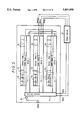
FIG. 1 shows a conventional linear sensor. The conventional linear sensor includes three rows 11 to 13 which are arranged in the vertical direction (V-direction). Each of the sensor rows has a predetermined number of pixels one-dimensionally arranged in the horizontal direction (H-direction). Analog shift registers (hereinafter, called the HCCDs) 21 to 23 are formed of CCDs (Charge Coupled Devices) for transferring signal charges in the H-direction. Shift gates 31 to 33 are formed for shifting the signal charges accumulated in the pixels of the sensor rows 11 to 13 to the HCCDs 21 to 23.
The signal charges transferred by the HCCDs 21 to 23 are converted (or reset) into a voltage by, for example, charge/voltage converter units 51 to 53 of a floating diffusion amplifier provided at the output of the HCCDs 21 to 23. Switches SW1 to SW3 are provided at the output sides of the charge/voltage converter units 51 to 53. These switches SW1 to SW3 are controlled to be sequentially changed in their positions, so that the signals are output from the rows in order.
FIG. 2 shows a timing chart of two different-phase horizontal clocks Φ1, Φ2, read-out pulses Φrog1 to Φrog3 for shift gates 31 to 33 and an output signal Vout, which are indicated in FIG. 1. The period tint is the signal charge accumulating time for each row.
As described above, in the conventional three-row linear sensor in which the output signals from the rows are output from one place, the switches SW1 to SW3 must provided at the output sides of the HCCDs 21 to 23 and to switch the output signals from the rows. Therefore, when the output signals are to be continuously read, it is necessary to shift the sampling times for the optical signals on the rows. The image information on the three rows cannot be two-dimensionally sampled at substantially a same time.
FIG. 3 shows another conventional linear sensor. As shown this figure, several to several tens of pixels of each row are shaded to be optical black (OPB). The outputs from the OPB pixels are used to clamp for the black level correction.
FIG. 4 shows a timing chart of two different-phase horizontal clocks Φ1, Φ2, read-out pulses Φrog1 to Φrog3 for shift gates 31 to 33 and an output signal Vout, which are indicated in FIG. 3. The period tint is the signal charge accumulating time for each row.
When the number of pixels of each row is large, or when the transfer speed is slow, however, the HCCDs 21 to 23 cause undesirable dark current components. The signals from the pixels more separated from the OPB pixels in the horizontal direction have lower S/N ratios due to the dark current components.
SUMMARY OF THE INVENTION
In view of the circumstances mentioned, it is an object of the present invention to provide an improved linear sensor which is capable of sampling image signals on a plurality of rows substantially at a same time.
It is another object of the present invention to provide an improved linear sensor capable of improving the S/N ratio of the image signals.
In one aspect of the present invention, a linear sensor for sampling signals produced by vertically opposed pixels of sensor rows substantially at a same time includes a plurality of sensor rows which are vertically arranged, a plurality of horizontal transfer registers which are provided to opposed sensor rows, a plurality of shift gates for transferring accumulated signal charges to the horizontal transfer registers, a vertical transfer register which is provided at one end of the horizontal transfer registers, a charge/voltage converter unit which is provided at the output of the vertical transfer register, and driver means for driving the shift gates, the horizontal transfer registers and the vertical transfer register.
In another aspect of the present invention, the linear sensor mentioned above further includes at least one sensor row of the plurality of sensor rows which is provided at the output side of the vertical transfer register and is optically shielded.
In still another aspect of the present invention, a linear sensor for sampling signals produced by vertically opposed pixels of sensor rows substantially at a time includes a plurality of sensor rows which are vertically arranged, a plurality of horizontal transfer registers which are provided to opposed sensor rows, a plurality of shift gates for transferring accumulated signal charges to the horizontal transfer registers, a plurality of charge/voltage converter units which are provide at the outputs of the each horizontal transfer register, driver means for driving the shift gates and the horizontal transfer registers, at least one sensor row of the plurality of sensor rows which is optically shielded, and a plurality of switch means which are provided at the outputs of the each charge/voltage converter.
In accordance with the present invention, the vertical transfer register is provided at one end of the horizontal transfer registers, and the signal charges of the pixels of the sensor rows are simultaneously read-out and transferred to the horizontal transfer registers by the shift gates at the trailing edges of the read-out pulse ΦROG. Thus, the vertically opposite pixels of the rows arranged in the vertical direction can be sampled at substantially a same time, and hence the signal charges of all the pixels of the rows can be two-dimensionally sampled at a time.
In addition, the charge/voltage converter unit is provided at the output of the vertical transfer register and the charge/voltage converter unit is shared by the respective rows. So, there is no need to provide the charge/voltage converter units at the rows, respectively. Therefore, it is possible to reduce the irregularity of the signal levels among the rows which is caused by the unequal characteristics of the charge/voltage converter units.
BRIEF DESCRIPTION OF THE DRAWINGS
The invention will be more readily understood with reference to the accompanying drawings, wherein:
FIG. 1 shows a construction diagram of a conventional linear sensor;
FIG. 2 shows a timing chart for explaining the operation of the conventional linear sensor;
FIG. 3 shows a construction diagram of another conventional linear sensor;
FIG. 4 shows a timing chart for explaining the operation of the another conventional linear sensor;
FIG. 5 shows a construction diagram of a first embodiment representing a linear sensor of the present invention;
FIG. 6 shows a timing chart for explaining the operation of the first embodiment of the present invention;
FIG. 7 shows a construction diagram of a second embodiment representing a linear sensor of the present invention;
FIG. 8 shows a timing chart for explaining the operation of the second embodiment of the present invention;
FIG. 9 shows a construction diagram of a third embodiment representing a linear sensor of the present invention;
FIG. 10 shows a block diagram of a modification of the resent invention;
FIG. 11 shows a construction diagram of a linear sensor showing a color coding of each row.
DETAILED DESCRIPTION OF THE PREFERRED EMBODIMENTS
The preferred embodiments of the present invention will be described in detail by referring to FIGS. 5 to 11. In these drawings, the same reference numerals are utilized as shown in FIGS. 1 to 4 so far as the same portions are referred.
FIG. 5 shows the construction diagram of a first embodiment representing a linear sensor of the present invention. In this embodiment, three rows 11 to 13 are arranged in the vertical direction (V-direction). Each of the sensor rows has a predetermined number of pixels one-dimensionally arranged in the horizontal direction (H-direction). Analog shift registers (hereinafter, called the HCCDs) 21 to 23 are formed of CCDs (Charge Coupled Devices) for transferring signal charges in the H-direction. Shift gates 31 to 33 are formed for shifting the signal charges accumulated in the pixels of the sensor rows 11 to 13 to the HCCDs 21 to 23. An analog vertical shift register (hereinafter, called the VCCD) 4 is provided at one end of the HCCDs 21 to 23 so that signal charges transferred by the HCCDs 21 to 23 can be sequentially transferred in the V-direction by the VCCD.
The signal charge transferred by the VCCD 4 is converted (or reset) into a voltage by, for example, a charge/voltage converter unit 5 of a floating diffusion amplifier provided at the output of the VCCD 4. The output voltage from the charge/voltage converter unit 5 is output at the outside as a sensor output Vout from the three rows.
Moreover, a drive circuit 6 including a timing generator (not shown) is provided to drive the HCCDs 21 to 23, shift gates 31 to 33, and VCCD 4. This drive circuit 6 supplies a plurality of horizontal transfer clocks of different phases (two phases in this embodiment), ΦH1, ΦH2, to all the three HCCDs 21 to 23, a read-out gate pulse ΦROG to all the three shift gates 31 to 33, and a plurality of vertical transfer clocks of different phases (two different phases in this embodiment), ΦV1, ΦV2, to the VCCD 4.
The frequency of the vertical transfer clocks ΦV1, ΦV2 is set to be higher than that of the horizontal transfer clocks ΦH1, ΦH2.
The operation of the three-row linear sensor of the above construction will be described with reference to the timing chart of FIG. 6.
First, the signal charge accumulated in the pixels of the three sensor rows 11 to 13 are simultaneously transferred to the HCCDs 21 to 23 by the shift gates 31 to 33 at the trailing edges of the read-out pulse ΦROG. Thus, the signal charges of all the pixels of the three rows are two-dimensionally sampled at substantially a same time.
When the signal charges have been completely transferred to the HCCDs 21 to 23 at substantially a same time, the signal charges are sequentially transferred to the VCCD 4 by the HCCDs 21 to 23 in response to the two horizontal transfer clocks ΦH1, ΦH2 of different phases. The signal charges of the VCCD 4 are vertically transferred by the two different-phase vertical transfer clocks ΦV1, ΦV2 of a higher frequency than the horizontal transfer clocks ΦH1, ΦH2.
Then, the vertically transferred charges are converted into a voltage by the charge/voltage converter unit 5 and produced as the output Vout. In this case, the signal of the leftmost pixel (D1-1) of the first row is produced first, and then the signal of the leftmost pixel (D2-1) of the second row is produced, followed by the signal charge of the leftmost pixel (D3-1) of the third row.
Then, the signal of the second pixel (D1-2) of the first row, when counting from the left end, is produced, followed by the signal of the second pixel (D2-2) of the second row, and the signal of the second pixel (D3-2) of the third row.
Similarly, the signals of the pixels of the vertically arranged rows are sequentially produced in a repetitive manner.
FIG. 7 shows the construction diagram of a second embodiment representing a linear sensor of the present invention. In comparison with the foregoing linear sensor of FIG. 5, this embodiment is different in that a sensor row 10, a HCCD 20 and a shift gate 30 are formed at the output of the VCCD 4. Other structures are the same. The sensor row 10 is formed of a black row optically shielded by an Aluminum-shading film or the like. The image signal from the black row is used for the black level correction. While one black row is provided in this embodiment, a plurality of black rows may be naturally provided.
As shown in FIG. 8, the vertically transferred charges are converted into a voltage by the charge/voltage converter unit 5 and produced as the output Vout. In this case, the signal of the leftmost pixel (B1) of the black row is produced first, and then the signal of the leftmost pixel (D1-1) of the first row is produced, followed by the signal charge of the leftmost pixel (D2-1) of the second row and the signal of the leftmost pixel (D3-1) of the third row.
Then, the signal of the second pixel (B2) of the black row, when counting from the left end, is produced, followed by the signal of the second pixel (D1-2) of the first row, the signal of the second pixel (D2-2) of the second row, and the signal of the second pixel (D3-2) of the third row.
Similarly, the signals of the pixels of the vertically arranged rows are sequentially produced in a repetitive manner.
As it is obvious from the waveform of the output Vout shown in FIG. 8, since the optically shielded sensor row 10 is provided at the output of the VCCD 4, the signal of the black row is produced before the signals of the pixels of the vertically arranged rows. Thus the black level correction can be performed on the basis of this black signal. When the black row signal is output, each black signal contains different dark current component which depend on the charge transfer time difference of the pixels of the black row. Since the charge of the pixel closer to the right end of the black row has the longer transfer time, the dark current component is large. Therefore, by clamping the black signal produced from each pixel, it is possible to more precisely correct the black level, and improve the S/N ratio of the image signal. The clamping for the black level correction may be made either within the sensor chip or in the outside.
FIG. 9 shows the construction diagram of a third embodiment representing a linear sensor of the present invention. In this embodiment, as in the second embodiment, sensor rows 10 to 13 are arranged in the vertical direction. HCCDs 20 to 23 are formed for transferring signal charges in the H-direction. Shift gates 30 to 33 are formed for shifting the signal charges accumulated in the pixels of the sensor rows 10 to 13 to the HCCDs 20 to 23. Of the four sensor rows 10 to 13, the top sensor row 10 is optically shielded to be the black line for the black level correction.
The signal charges transferred by the HCCDs 20 to 23 of the rows are converted into voltages by the charge/voltage converter units 50 to 53 which are provided at the outputs of the HCCDs 20 to 23. The output voltage from the charge/voltage converter units 50 to 53 are output as the output Vout by switches SW0 to SW3.
According to this construction, the black signal of one row can be output. So, the black output can be clamped for black level correction at each pixel corresponding vertically to each rows. Thus, as is similar to the second embodiment, even if difference of the dark current components depend on the horizontal transfer time difference, the black level correction can be more accurately carried out. Therefore, the S/N ratio of the image signal can be improved.
While only one black row is provided in this embodiment, a plurality of black rows may be of course provided. In addition, while the black row is provided on the top in FIG. 9, it may be provided between the three rows for image information. In this case, since the black signal is used as a reference for the black level correction, the switches SW0 to SW3 must be controlled to operate so that the black signal can be produced before the outputs from the other three rows.
According to the above constructions, as will be obvious from the waveforms of the output Vout shown in FIGS. 6 and 8, the image signals from the respective rows are alternately produced.
As shown in FIG. 10, a sampling circuit 7 may be provided as an external circuit. The sampling circuit 7 samples the output Vout at predetermined intervals, and rearranges the pixel signals at each row, converting them into a television signal.
In addition, the linear sensor of the present invention can be used as a color linear sensor. In this case, each of the three sensor rows 11 to 13 has trios of primary color dots (R, G, B) arranged in a dot-sequential manner so that the same color dots are aligned in the V-direction as shown in FIG. 11. Thus, the same color pixel signals of the three rows can be produced together as the output Vout.
While specific embodiments of the invention have been shown and disclosed, it is to be understood that numerous changes and modifications may be made by those skilled in the art without departing from the scope and intent of the invention.

Claims (7)

What is claimed is:
1. A sensor for sampling pixels of a plurality of vertically arranged sensor rows substantially at a same time comprising:
a plurality of sensor rows vertically arranged, each sensor row having a plurality of horizontally arranged pixels;
a plurality of horizontal transfer registers provided to oppose said plurality of sensor rows for transferring signal charges in the horizontal direction;
a plurality of shift gates for transferring said signal charges accumulated in the pixels of said plurality of sensor rows to said plurality of horizontal transfer registers substantially at a same time;
a charge/voltage converter unit provided at the output of each horizontal transfer register;
drive means for driving said shift gates, and said horizontal transfer registers;
at least one sensor row of said plurality of sensor rows, being optically shielded; and
a switch means provided at the output of each charge/voltage converter, wherein said switch means are controlled to operate so that said signal charges accumulated in said vertically opposed pixels of said plurality of vertically arranged sensor rows are sequentially output in a repetitive manner.
2. A linear sensor according to claim 1, wherein said switch means are controlled to operate so that said signal charge of said at least one optically shielded sensor row are output before the outputs from the other rows.
3. A linear sensor according to claim 1, wherein said sensor rows, said horizontal transfer registers and said shift registers are each provided for four rows.
4. A linear sensor according to claim 1, wherein each of the plurality of sensor rows except for said at least one optically shielded sensor row has primary color dot trios arranged in a dot-sequential manner.
5. A linear sensor according to claim 1, wherein the outputs from said each charge/voltage converter unit are sampled to produce a television signal for said plurality of sensor rows.
6. A linear sensor according to claim 1, wherein said plurality of shift gates are used to read-out said signal charges accumulated in all the pixels of said plurality of sensor rows and transfer said signal charges to said plurality of horizontal transfer registers at a time.
7. The sensor of claim 1, further comprising means for correcting a signal level of said pixels by adjusting said signal level with reference to a level from a charge of a corresponding pixel from the at least one shielded row.
US08/677,471 1992-03-19 1996-07-10 Linear sensor having a plurality of sensor rows Expired - Lifetime US5801850A (en)

Priority Applications (1)

Application Number Priority Date Filing Date Title
US08/677,471 US5801850A (en) 1992-03-19 1996-07-10 Linear sensor having a plurality of sensor rows

Applications Claiming Priority (6)

Application Number Priority Date Filing Date Title
JP4093386A JPH05268524A (en) 1992-03-19 1992-03-19 Solid-state image pickup device
JP4-093387 1992-03-19
JP4-093386 1992-03-19
JP4093387A JP3064657B2 (en) 1992-03-19 1992-03-19 Solid-state imaging device
US08/033,364 US5539536A (en) 1992-03-19 1993-03-18 Linear imaging sensor having improved charged transfer circuitry
US08/677,471 US5801850A (en) 1992-03-19 1996-07-10 Linear sensor having a plurality of sensor rows

Related Parent Applications (1)

Application Number Title Priority Date Filing Date
US08/033,364 Division US5539536A (en) 1992-03-19 1993-03-18 Linear imaging sensor having improved charged transfer circuitry

Publications (1)

Publication Number Publication Date
US5801850A true US5801850A (en) 1998-09-01

Family

ID=26434768

Family Applications (2)

Application Number Title Priority Date Filing Date
US08/033,364 Expired - Lifetime US5539536A (en) 1992-03-19 1993-03-18 Linear imaging sensor having improved charged transfer circuitry
US08/677,471 Expired - Lifetime US5801850A (en) 1992-03-19 1996-07-10 Linear sensor having a plurality of sensor rows

Family Applications Before (1)

Application Number Title Priority Date Filing Date
US08/033,364 Expired - Lifetime US5539536A (en) 1992-03-19 1993-03-18 Linear imaging sensor having improved charged transfer circuitry

Country Status (1)

Country Link
US (2) US5539536A (en)

Cited By (12)

* Cited by examiner, † Cited by third party
Publication number Priority date Publication date Assignee Title
US5969830A (en) * 1996-05-30 1999-10-19 Nec Corporation Color linear image sensor and driving method therefor
US6400404B2 (en) * 1996-07-12 2002-06-04 Sony Corporation Solid-state imaging device and camera using the same
US20020154231A1 (en) * 1998-07-17 2002-10-24 Steven Decker Image sensor using multiple array readout lines
US6476941B1 (en) * 1997-04-02 2002-11-05 Canon Kabushiki Kaisha Solid-state image sensing device and operation method thereof
US6480228B1 (en) * 1995-07-10 2002-11-12 Sony Corporation Solid-state image sensing device
US6570615B1 (en) * 1998-07-14 2003-05-27 Analog Devices, Inc. Pixel readout scheme for image sensors
US20030103152A1 (en) * 2000-09-26 2003-06-05 Rohm Co., Ltd. Image reading device
US20040119857A1 (en) * 2002-09-12 2004-06-24 Andreas Loew Method for the correction of video signals
US20040130642A1 (en) * 2002-12-20 2004-07-08 Matsushita Electric Industrial Co., Ltd. Solid-state image pickup device, drive method therefor and camera
US6924840B1 (en) * 1998-06-24 2005-08-02 Seiko Epson Corporation Color image capturing device and image reader using the color image capturing device
KR100528691B1 (en) * 1998-12-16 2006-02-28 엘지.필립스 엘시디 주식회사 Apparatus for Taking Image
US20060227234A1 (en) * 2003-03-21 2006-10-12 Atmel Grenoble Image sensor with rapid read cycle

Families Citing this family (7)

* Cited by examiner, † Cited by third party
Publication number Priority date Publication date Assignee Title
US5539536A (en) * 1992-03-19 1996-07-23 Sony Corporation Linear imaging sensor having improved charged transfer circuitry
JP2870454B2 (en) * 1995-06-16 1999-03-17 日本電気株式会社 Color linear image sensor
US6169576B1 (en) * 1996-06-18 2001-01-02 Kabushiki Kaisha Toshiba Solid state image sensing device having variable resolution and color linear image sensor having variable resolution and control method thereof
JPH10233883A (en) * 1996-12-20 1998-09-02 Seiko Epson Corp Ccd image pickup device and image reader
JP3899627B2 (en) * 1998-01-06 2007-03-28 富士ゼロックス株式会社 Linear image sensor, image reading apparatus, and charge transfer method
JP4450941B2 (en) * 2000-04-12 2010-04-14 富士通マイクロエレクトロニクス株式会社 Solid-state imaging device, image processing apparatus, and image processing method
JP4341177B2 (en) * 2000-12-15 2009-10-07 ソニー株式会社 Solid-state imaging device, driving method thereof, and image reading device

Citations (4)

* Cited by examiner, † Cited by third party
Publication number Priority date Publication date Assignee Title
US4641183A (en) * 1982-07-16 1987-02-03 Canon Kabushiki Kaisha Image pick-up apparatus
US4996600A (en) * 1988-06-08 1991-02-26 Nippon Hoso Kyokai Two dimensional solid state image sensing device
US5539536A (en) * 1992-03-19 1996-07-23 Sony Corporation Linear imaging sensor having improved charged transfer circuitry
US5648667A (en) * 1994-06-14 1997-07-15 Nec Corporation Image pickup device with and image pickup method by use of two-dimensionally arranged sensors having sensitivities different in certain direction of arrangement

Family Cites Families (9)

* Cited by examiner, † Cited by third party
Publication number Priority date Publication date Assignee Title
JPS5930376A (en) * 1982-08-13 1984-02-17 Olympus Optical Co Ltd Solid-state image pickup device
US4758734A (en) * 1984-03-13 1988-07-19 Nec Corporation High resolution image sensor array using amorphous photo-diodes
DE3615342A1 (en) * 1985-05-08 1986-11-13 Fuji Photo Film Co., Ltd., Minami-Ashigara, Kanagawa COLOR IMAGE SENSOR
JPS6238677A (en) * 1985-08-13 1987-02-19 Mitsubishi Electric Corp Solid-state image pickup device
GB2186149B (en) * 1985-12-23 1989-10-18 Dr John Gordon Rushbrooke Improvements in and relating to x-ray analysis systems
JP2656475B2 (en) * 1986-10-01 1997-09-24 株式会社日立製作所 Solid-state imaging device
EP0419118B1 (en) * 1989-09-14 1995-07-12 Sony Corporation Charge coupled device imager with horizontal charge transfer sections in an imaging section
JP2873046B2 (en) * 1990-05-01 1999-03-24 チノン株式会社 Image signal processing device
JP3065396B2 (en) * 1991-10-07 2000-07-17 ローム株式会社 Image sensor

Patent Citations (4)

* Cited by examiner, † Cited by third party
Publication number Priority date Publication date Assignee Title
US4641183A (en) * 1982-07-16 1987-02-03 Canon Kabushiki Kaisha Image pick-up apparatus
US4996600A (en) * 1988-06-08 1991-02-26 Nippon Hoso Kyokai Two dimensional solid state image sensing device
US5539536A (en) * 1992-03-19 1996-07-23 Sony Corporation Linear imaging sensor having improved charged transfer circuitry
US5648667A (en) * 1994-06-14 1997-07-15 Nec Corporation Image pickup device with and image pickup method by use of two-dimensionally arranged sensors having sensitivities different in certain direction of arrangement

Cited By (30)

* Cited by examiner, † Cited by third party
Publication number Priority date Publication date Assignee Title
US20090278972A1 (en) * 1995-07-10 2009-11-12 Sony Corporation Solid-state image sensing device
US6480228B1 (en) * 1995-07-10 2002-11-12 Sony Corporation Solid-state image sensing device
US20070052828A1 (en) * 1995-07-10 2007-03-08 Sony Corporation Solid-state image sensing device
US20060250512A1 (en) * 1995-07-10 2006-11-09 Sony Corporation Solid-state image sensing device
US20090256944A1 (en) * 1995-07-10 2009-10-15 Sony Corporation Solid-State Image Sensing Device
US7893982B2 (en) 1995-07-10 2011-02-22 Sony Corporation Solid-state image sensing device
US20030030736A1 (en) * 1995-07-10 2003-02-13 Satoshi Yoshihara Solid-state image sensing device
US7589776B2 (en) 1995-07-10 2009-09-15 Sony Corporation Solid-state image sensing device
US8159590B2 (en) 1995-07-10 2012-04-17 Sony Corporation Solid-state image sensing device
US7535507B2 (en) 1995-07-10 2009-05-19 Sony Corporation Solid-state image sensing device
US7071977B2 (en) * 1995-07-10 2006-07-04 Sony Corporation Solid-state image sensing device
US20050151865A1 (en) * 1995-07-10 2005-07-14 Sony Corporation Solid-state image sensing device
US7573521B2 (en) 1995-07-10 2009-08-11 Sony Corporation Solid-state image sensing device
US5969830A (en) * 1996-05-30 1999-10-19 Nec Corporation Color linear image sensor and driving method therefor
US6400404B2 (en) * 1996-07-12 2002-06-04 Sony Corporation Solid-state imaging device and camera using the same
US6476941B1 (en) * 1997-04-02 2002-11-05 Canon Kabushiki Kaisha Solid-state image sensing device and operation method thereof
US6924840B1 (en) * 1998-06-24 2005-08-02 Seiko Epson Corporation Color image capturing device and image reader using the color image capturing device
US6570615B1 (en) * 1998-07-14 2003-05-27 Analog Devices, Inc. Pixel readout scheme for image sensors
US7242428B2 (en) 1998-07-17 2007-07-10 Analog Devices, Inc. Image sensor using multiple array readout lines
US6512546B1 (en) 1998-07-17 2003-01-28 Analog Devices, Inc. Image sensor using multiple array readout lines
US20020154231A1 (en) * 1998-07-17 2002-10-24 Steven Decker Image sensor using multiple array readout lines
KR100528691B1 (en) * 1998-12-16 2006-02-28 엘지.필립스 엘시디 주식회사 Apparatus for Taking Image
US7298403B2 (en) * 2000-09-26 2007-11-20 Rohm Co., Ltd. Image reading device
US20030103152A1 (en) * 2000-09-26 2003-06-05 Rohm Co., Ltd. Image reading device
US7508435B2 (en) * 2002-09-12 2009-03-24 Thomson Licensing Method for the correction of video signals
US20040119857A1 (en) * 2002-09-12 2004-06-24 Andreas Loew Method for the correction of video signals
US20040130642A1 (en) * 2002-12-20 2004-07-08 Matsushita Electric Industrial Co., Ltd. Solid-state image pickup device, drive method therefor and camera
US7701498B2 (en) * 2002-12-20 2010-04-20 Panasonic Corporation Solid-state image pickup device, drive method therefor and camera
US7471323B2 (en) * 2003-03-21 2008-12-30 Atmel Grenoble Image sensor with rapid read cycle
US20060227234A1 (en) * 2003-03-21 2006-10-12 Atmel Grenoble Image sensor with rapid read cycle

Also Published As

Publication number Publication date
US5539536A (en) 1996-07-23

Similar Documents

Publication Publication Date Title
US5801850A (en) Linear sensor having a plurality of sensor rows
US7430006B2 (en) Charge transfer device and a driving method thereof and a driving method for solid-state image sensing device
US4837630A (en) Solid-state imaging apparatus with a plurality of CCD storage sections
US4598321A (en) CCD imagers with registers partitioned for simultaneous charge transfers in opposing directions
US4635122A (en) Image pickup device of the frame transfer type and image pickup arrangement using the same
US7289150B2 (en) Solid-state image apparatus including a plurality of horizontal transfer registers for transferring image signals from an imaging area
US5340977A (en) Solid-state image pickup device
US5043817A (en) Image pick-up apparatus with electronic zooming-in
JPS60187187A (en) Solid-state image pickup device and its driving method
US5796432A (en) Method of and apparatus for solid state imaging device
US4244003A (en) Charge proportional opto-electronic converter providing enhanced blue color signal
US7697048B2 (en) Solid state imaging apparatus and driving method of the solid state imaging apparatus using four pixel addition
US5500675A (en) Method of driving solid-state image sensing device
US4866528A (en) Image pickup apparatus providing lessened flicker in electronic still cameras and the like
US4853786A (en) CSD image sensor and method of decreasing smear by the user thereof
KR100248616B1 (en) Linear sensor having a plurality of sensor rows
US5523787A (en) Solid-state imaging device adapted for an interlaced scanning and a non-interlaced scanning and method for driving same
US4791307A (en) Method for reading out charges in solid-state image pickup unit
JP2544341B2 (en) Driving method for solid-state imaging device
JP3064657B2 (en) Solid-state imaging device
KR100262288B1 (en) Solid state image pick-up device and its driving method
JP3481822B2 (en) Solid-state imaging device and color linear image sensor
JPH09205520A (en) Three-line linear sensor
JPH0370375A (en) Driving method for solid-stage pickup element
JP2666398B2 (en) Solid-state imaging device and driving method thereof

Legal Events

Date Code Title Description
STCF Information on status: patent grant

Free format text: PATENTED CASE

FEPP Fee payment procedure

Free format text: PAT HOLDER CLAIMS SMALL ENTITY STATUS, ENTITY STATUS SET TO SMALL (ORIGINAL EVENT CODE: LTOS); ENTITY STATUS OF PATENT OWNER: LARGE ENTITY

FPAY Fee payment

Year of fee payment: 4

REFU Refund

Free format text: REFUND - SURCHARGE, PETITION TO ACCEPT PYMT AFTER EXP, UNINTENTIONAL (ORIGINAL EVENT CODE: R2551); ENTITY STATUS OF PATENT OWNER: LARGE ENTITY

FEPP Fee payment procedure

Free format text: PETITION RELATED TO MAINTENANCE FEES FILED (ORIGINAL EVENT CODE: PMFP); ENTITY STATUS OF PATENT OWNER: LARGE ENTITY

FEPP Fee payment procedure

Free format text: PETITION RELATED TO MAINTENANCE FEES GRANTED (ORIGINAL EVENT CODE: PMFG); ENTITY STATUS OF PATENT OWNER: LARGE ENTITY

PRDP Patent reinstated due to the acceptance of a late maintenance fee

Effective date: 20030623

FEPP Fee payment procedure

Free format text: PAT HOLDER NO LONGER CLAIMS SMALL ENTITY STATUS, ENTITY STATUS SET TO UNDISCOUNTED (ORIGINAL EVENT CODE: STOL); ENTITY STATUS OF PATENT OWNER: LARGE ENTITY

REFU Refund

Free format text: REFUND - PAYMENT OF MAINTENANCE FEE, 8TH YR, SMALL ENTITY (ORIGINAL EVENT CODE: R2552); ENTITY STATUS OF PATENT OWNER: LARGE ENTITY

FPAY Fee payment

Year of fee payment: 8

FEPP Fee payment procedure

Free format text: PAYOR NUMBER ASSIGNED (ORIGINAL EVENT CODE: ASPN); ENTITY STATUS OF PATENT OWNER: LARGE ENTITY

Free format text: PAYER NUMBER DE-ASSIGNED (ORIGINAL EVENT CODE: RMPN); ENTITY STATUS OF PATENT OWNER: LARGE ENTITY

FPAY Fee payment

Year of fee payment: 12