US5808708A - Lighting apparatus - Google Patents
Lighting apparatus Download PDFInfo
- Publication number
- US5808708A US5808708A US08/573,498 US57349895A US5808708A US 5808708 A US5808708 A US 5808708A US 57349895 A US57349895 A US 57349895A US 5808708 A US5808708 A US 5808708A
- Authority
- US
- United States
- Prior art keywords
- light
- section
- light source
- light emitting
- lighting apparatus
- Prior art date
- Legal status (The legal status is an assumption and is not a legal conclusion. Google has not performed a legal analysis and makes no representation as to the accuracy of the status listed.)
- Expired - Lifetime
Links
Images


Classifications
-
- G—PHYSICS
- G02—OPTICS
- G02F—OPTICAL DEVICES OR ARRANGEMENTS FOR THE CONTROL OF LIGHT BY MODIFICATION OF THE OPTICAL PROPERTIES OF THE MEDIA OF THE ELEMENTS INVOLVED THEREIN; NON-LINEAR OPTICS; FREQUENCY-CHANGING OF LIGHT; OPTICAL LOGIC ELEMENTS; OPTICAL ANALOGUE/DIGITAL CONVERTERS
- G02F1/00—Devices or arrangements for the control of the intensity, colour, phase, polarisation or direction of light arriving from an independent light source, e.g. switching, gating or modulating; Non-linear optics
- G02F1/01—Devices or arrangements for the control of the intensity, colour, phase, polarisation or direction of light arriving from an independent light source, e.g. switching, gating or modulating; Non-linear optics for the control of the intensity, phase, polarisation or colour
- G02F1/13—Devices or arrangements for the control of the intensity, colour, phase, polarisation or direction of light arriving from an independent light source, e.g. switching, gating or modulating; Non-linear optics for the control of the intensity, phase, polarisation or colour based on liquid crystals, e.g. single liquid crystal display cells
- G02F1/133—Constructional arrangements; Operation of liquid crystal cells; Circuit arrangements
- G02F1/1333—Constructional arrangements; Manufacturing methods
- G02F1/1335—Structural association of cells with optical devices, e.g. polarisers or reflectors
-
- G—PHYSICS
- G02—OPTICS
- G02B—OPTICAL ELEMENTS, SYSTEMS OR APPARATUS
- G02B6/00—Light guides; Structural details of arrangements comprising light guides and other optical elements, e.g. couplings
- G02B6/0001—Light guides; Structural details of arrangements comprising light guides and other optical elements, e.g. couplings specially adapted for lighting devices or systems
- G02B6/0011—Light guides; Structural details of arrangements comprising light guides and other optical elements, e.g. couplings specially adapted for lighting devices or systems the light guides being planar or of plate-like form
- G02B6/0013—Means for improving the coupling-in of light from the light source into the light guide
- G02B6/0015—Means for improving the coupling-in of light from the light source into the light guide provided on the surface of the light guide or in the bulk of it
- G02B6/0018—Redirecting means on the surface of the light guide
-
- G—PHYSICS
- G02—OPTICS
- G02B—OPTICAL ELEMENTS, SYSTEMS OR APPARATUS
- G02B6/00—Light guides; Structural details of arrangements comprising light guides and other optical elements, e.g. couplings
- G02B6/24—Coupling light guides
- G02B6/42—Coupling light guides with opto-electronic elements
- G02B6/4298—Coupling light guides with opto-electronic elements coupling with non-coherent light sources and/or radiation detectors, e.g. lamps, incandescent bulbs, scintillation chambers
-
- G—PHYSICS
- G02—OPTICS
- G02B—OPTICAL ELEMENTS, SYSTEMS OR APPARATUS
- G02B6/00—Light guides; Structural details of arrangements comprising light guides and other optical elements, e.g. couplings
- G02B6/0001—Light guides; Structural details of arrangements comprising light guides and other optical elements, e.g. couplings specially adapted for lighting devices or systems
- G02B6/0011—Light guides; Structural details of arrangements comprising light guides and other optical elements, e.g. couplings specially adapted for lighting devices or systems the light guides being planar or of plate-like form
- G02B6/0013—Means for improving the coupling-in of light from the light source into the light guide
- G02B6/0015—Means for improving the coupling-in of light from the light source into the light guide provided on the surface of the light guide or in the bulk of it
- G02B6/002—Means for improving the coupling-in of light from the light source into the light guide provided on the surface of the light guide or in the bulk of it by shaping at least a portion of the light guide, e.g. with collimating, focussing or diverging surfaces
-
- G—PHYSICS
- G02—OPTICS
- G02F—OPTICAL DEVICES OR ARRANGEMENTS FOR THE CONTROL OF LIGHT BY MODIFICATION OF THE OPTICAL PROPERTIES OF THE MEDIA OF THE ELEMENTS INVOLVED THEREIN; NON-LINEAR OPTICS; FREQUENCY-CHANGING OF LIGHT; OPTICAL LOGIC ELEMENTS; OPTICAL ANALOGUE/DIGITAL CONVERTERS
- G02F1/00—Devices or arrangements for the control of the intensity, colour, phase, polarisation or direction of light arriving from an independent light source, e.g. switching, gating or modulating; Non-linear optics
- G02F1/01—Devices or arrangements for the control of the intensity, colour, phase, polarisation or direction of light arriving from an independent light source, e.g. switching, gating or modulating; Non-linear optics for the control of the intensity, phase, polarisation or colour
- G02F1/13—Devices or arrangements for the control of the intensity, colour, phase, polarisation or direction of light arriving from an independent light source, e.g. switching, gating or modulating; Non-linear optics for the control of the intensity, phase, polarisation or colour based on liquid crystals, e.g. single liquid crystal display cells
- G02F1/133—Constructional arrangements; Operation of liquid crystal cells; Circuit arrangements
- G02F1/1333—Constructional arrangements; Manufacturing methods
- G02F1/1335—Structural association of cells with optical devices, e.g. polarisers or reflectors
- G02F1/1336—Illuminating devices
- G02F1/133615—Edge-illuminating devices, i.e. illuminating from the side
-
- Y—GENERAL TAGGING OF NEW TECHNOLOGICAL DEVELOPMENTS; GENERAL TAGGING OF CROSS-SECTIONAL TECHNOLOGIES SPANNING OVER SEVERAL SECTIONS OF THE IPC; TECHNICAL SUBJECTS COVERED BY FORMER USPC CROSS-REFERENCE ART COLLECTIONS [XRACs] AND DIGESTS
- Y10—TECHNICAL SUBJECTS COVERED BY FORMER USPC
- Y10S—TECHNICAL SUBJECTS COVERED BY FORMER USPC CROSS-REFERENCE ART COLLECTIONS [XRACs] AND DIGESTS
- Y10S385/00—Optical waveguides
- Y10S385/901—Illuminating or display apparatus
Definitions
- the present invention relates to a display device such as a liquid crystal display device having a light transmitting display screen and a lighting apparatus which is to be incorporated into the display device so as to light the display screen from the back, and more particularly to an edge-light type lighting apparatus having a light source arranged at an end section of a light guiding plate.
- a direct lighting apparatus having a plurality of light sources at the back of the liquid crystal panel and an edge-light type lighting apparatus having a light source at an end of a light guiding plate are known.
- the direct lighting apparatus has smaller outside dimensions than the edge-light type lighting apparatus, but suffers from such drawbacks that (1) reducing the thickness is difficult, (2) luminance spots tend to appear, and (3) the structure is complicated. For this reason, in recent years, the edge-light type lighting apparatus is used more than the direct lighting apparatus.
- the edge-light type lighting apparatus includes a light guiding plate 102, and light sources 101 which are disposed on both ends of the light guiding plate 102. Therefore, light emitted by the light source 101 strikes light-incidence end surface 102a and enters into the light guiding plate 102. The incident light is guided into the light guiding plate 102 while being reflected by a reflecting sheet 104 which is placed on the back surface of the light guiding plate 102, and is emitted toward a liquid crystal display panel (not shown) through a diffusing sheet 103 placed on the top surface of the light guiding plate 102.
- An area indicated by the arrows in FIG. 27 shows a region of the liquid crystal display panel where data is displayed.
- data display space R This region is hereinafter referred to as data display space R. Additionally, a portion of the light guiding plate 102 which irradiates light on the data display space R is a data display space corresponding section (hereinafter simply referred to as the corresponding section) 102b.
- the edge-light type lighting apparatus if the light source 101 and the light guiding plate 102 are disposed close to each other, the end portion of the light guiding plate 102 and the vicinity thereof are irradiated more strongly and become brighter than the central portion. This may cause luminance spots.
- a lighting apparatus which prevents the luminance spots from appearing on the light guiding plate 102 is disclosed in Japanese Publication for Unexamined Patent Application No. 88166/1993 (Tokukaihei 5-88166).
- the light-incidence end surface 102a of the light guiding plate 102 is made a convex surface having a curved profile like an arc of circle, and light that moves toward the vicinity of the end portion of the light guiding plate 102 is refracted using the effect of a convex lens so that the light moves toward the center portion.
- the lighting apparatus can prevent the end portion of the light guiding plate 102 from becoming brighter than the central portion with the irradiation of the light from the light source 101, and luminance spots from being generated.
- this structure shortens the distance between the light source 101 and the corresponding section 102b of the light guiding plate 102 to some degrees.
- the light sources 101 and the light guiding plate 102 are arranged on the same plane, the outside dimensions of the whole lighting apparatus become larger than the dimensions of the liquid crystal display panel (not shown) by an amount corresponding to the sizes of the light sources 101. Consequently, if such a lighting apparatus is incorporated into a liquid crystal display device, it becomes difficult to decrease the outside dimensions of the liquid crystal display device with respect to the area of the data display space to a desired level.
- Japanese Publication for Unexamined Patent Application No. 53111/1993 discloses a liquid crystal display device.
- the plate thickness of the corresponding section 102b of the light guiding plate 102 is thinner than that of the light-incidence end surface 102a, and the plate thickness of the light-incidence end surface 102a is substantially equal to the tube diameter of the light source 101.
- Japanese Publication for Unexamined Patent Application No. 249459/1993 discloses a liquid crystal display device. In the structure of this liquid crystal display device, as illustrated in FIG.
- each of the light sources 101 is disposed on the front surface of the end portion of the light guiding plate 102 and the liquid crystal display panel 106 is buried in a recessed portion 102c of the light guiding plate 102 so as to prevent the light from the light source 101 from affecting the area of the plane of incidence even when the thickness of the light guiding plate 102 is reduced.
- a lighting apparatus of the present invention includes:
- a light emitting section in the shape of a flat plate having a light emitting surface on one side, the light emitting section being made from a light transmitting material;
- a light source disposed on a side of the light emitting section opposite to the light emitting surface
- a light guiding section for guiding light from the light source into the light emitting section through a side surface of the light emitting section.
- the light guiding section can guide the light from the light source disposed on the back surface of the light emitting section to the side surface of the light emitting section and make the light incident on the light emitting section through the side surface. Namely, by disposing the light source, which is arranged along the side surface of the light emitting section in a prior art, on the back surface of the light emitting section, it is possible to reduce the area of the entire apparatus with respect to the area of the light emitting section. As a result, a lighting apparatus in which the ratio of the area of the light emitting section to the total area of the apparatus is high can be provided.
- the light guiding section includes:
- a light transmitting section formed by a light transmitting material so as to lie in a bent shape from the side surface of the light emitting section to a position facing the light source;
- the light-incidence end surface at a position of the light guiding section facing the light source, the light-incidence end surface being a plane substantially perpendicular to a surface opposite to the light emitting surface of the light emitting section but slightly tilts with respect to the surface opposite to the light emitting surface so that the plane is separated from the light source by a greater distance at a more distant point from the surface opposite to the light emitting surface.
- a display device having a light-transmitting-type image display panel and a lighting apparatus for irradiating the image display panel from the back includes:
- a light guiding member including a light emitting section in the shape of a flat plate having a surface whose size is substantially equal to the size of an image display space of the image display panel, and a light guiding section for guiding light from the light source to be incident on a side surface of the light emitting section,
- the light source is disposed on the back surface of the light emitting section of the light guiding member with respect to the image display panel so that at least a part of the light source is located in a position closer to the center of the light emitting section than to an edge of the light emitting section.
- the light source By disposing the light source on the back surface of the light emitting section in the shape of a flat plate having a surface whose size is substantially equal to the size of the image display panel and by causing the light guiding section to guide the light from the light source to the side surface of the light emitting section for emitting the light, it is possible to reduce the area of portions other than the image display space with respect to the total area of the device.
- FIG. 1 is a schematic cross section showing the structure of a liquid crystal display device incorporating a lighting apparatus according to one embodiment of the present invention.
- FIG. 2 is a perspective view showing the outer appearance of the lighting apparatus.
- FIG. 3 is a schematic cross section showing the structure of a liquid crystal display device incorporating a lighting apparatus as a modified example of the liquid crystal display device of FIG. 1.
- FIG. 4 is a schematic cross section showing the structure of a liquid crystal display device incorporating a lighting apparatus as another modified example of the liquid crystal display device of FIG. 1.
- FIG. 5 is a schematic cross section showing the structure of a liquid crystal display device incorporating a lighting apparatus as still another modified example of the liquid crystal display device of FIG. 1.
- FIG. 6 is a schematic cross section showing the structure of a liquid crystal display device incorporating a lighting apparatus according to another embodiment of the present invention.
- FIG. 7 is a perspective view showing the outer appearance of the lighting apparatus.
- FIG. 8 is a schematic cross section showing the structure of a liquid crystal display device incorporating a lighting apparatus as a modified example of the liquid crystal display device of FIG. 6.
- FIG. 9(a) is a view explaining the movement of light in a lighting apparatus as a comparable example of the present invention, in which a reflector is formed along the periphery of a bent section of a light guiding plate
- FIG. 9(b) is a view explaining the movement of light in the lighting apparatus of the present invention, in which a space is formed between a reflector and a bent section of a light guiding plate.
- FIG. 10 is a schematic cross section of the lighting apparatus as the comparable example of the present invention.
- FIG. 11 is a schematic cross section of a liquid crystal display device incorporating a lighting apparatus according to still another embodiment of the present invention.
- FIG. 12 is a perspective view showing the outer appearance of the lighting apparatus of FIG. 11.
- FIG. 13 is a schematic cross section of a lighting apparatus as a comparable example of the present invention.
- FIG. 14(a) shows the movement of light in the comparable lighting apparatus of FIG. 13
- FIG. 14(b) shows the movement of light in the lighting apparatus of FIG. 11.
- FIG. 15 is a schematic cross section of a liquid crystal display device incorporating a lighting apparatus as a modified example of the liquid crystal display device of FIG. 11.
- FIG. 16(a) shows the movement of light in the comparable lighting apparatus of FIG. 13
- FIG. 16(b) shows the movement of light in the lighting apparatus of FIG. 15.
- FIG. 17 is a schematic cross section of a liquid crystal display device incorporating a lighting apparatus as another modified example of the liquid crystal display device of FIG. 11.
- FIG. 18(a) shows the movement of light in the comparable lighting apparatus of FIG. 13
- FIG. 18(b) shows the movement of light in the lighting apparatus of FIG. 17.
- FIG. 19 is a schematic cross section of a liquid crystal display device incorporating a lighting apparatus according to yet another embodiment of the present invention.
- FIG. 20 is a perspective view showing the outer appearance of the lighting apparatus of FIG. 19.
- FIG. 21(a) shows the movement of light in a lighting apparatus as a comparable example of the present invention
- FIG. 21(b) shows the movement of light in the lighting apparatus of FIG. 19.
- FIG. 22 is a schematic cross section of a liquid crystal display device incorporating a lighting apparatus as a modified example of the lighting apparatus of FIG. 19.
- FIG. 23(a) shows the movement of light in the lighting apparatus as the comparable example of the present invention
- FIG. 23(b) shows the movement of light in the lighting apparatus of FIG. 22.
- FIG. 24 is a schematic cross section of a liquid crystal display device incorporating a lighting apparatus as another modified example of the liquid crystal display device of FIG. 19.
- FIG. 25(a) shows the movement of light in a lighting apparatus as the comparable example of the present invention
- FIG. 25(b) shows the movement of light in the lighting apparatus of FIG. 24.
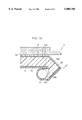
- FIG. 26 is a view schematically showing the structure of a conventional edge-light type lighting apparatus.
- FIG. 27 is a view schematically showing the structure of a conventional edge-light type lighting apparatus.
- FIG. 28 is a view schematically showing the structure of a conventional edge-light type lighting apparatus.
- FIG. 29 is a view schematically showing the structure of a conventional edge-light type lighting apparatus.
- a flat light source device 1 as a lighting apparatus of this embodiment for use in a liquid crystal display device is disposed behind the back surface of the flat liquid crystal display panel 2, and irradiates the liquid crystal display panel 2 from the back.
- the flat light source device 1 has an outer appearance shown in FIG. 2, and mainly includes two light sources 3, a light guiding plate 4 for guiding light from the light sources 3, and two reflectors 5.
- the reflector 5 reflects the light from the light source 3 so that the light falls on the light guiding plate 4 efficiently.
- the light source 3 is a linear light source, for example, a fluorescent tube, which is similar to a light source used in a conventional edge-light type lighting apparatus for a liquid crystal display device.
- the light guiding plate 4 is formed into the shape of a substantially flat plate by a material having high transmissivity with respect to every range of wavelength, for example, a transparent acrylic resin. As illustrated in FIGS. 1 and 2, an end portion of the light guiding plate 4 near the light source 3 is curved downward so as to have a substantially semicircular profile. The position at which the end portion is bent is located outside of the data display space R of the light crystal display panel 2 above the light guiding plate 4.
- a flat plate portion corresponding to the data display space R is a data display space corresponding section (hereinafter just referred to as the corresponding section) 4a.
- the bent end portion is a non-data-display space corresponding section (hereinafter referred to as the non-corresponding section) 4b.
- the bent portion of the non-corresponding section 4b has a light-incidence end surface 4c perpendicular to the liquid crystal display panel 2.
- the light source 3 is disposed behind the back surface of the light guiding plate 4 to face the light-incidence end surface 4c. Consequently, the light from the light source 3 falls on the light guiding plate 4 through the light-incidence end surface 4c.
- the non-corresponding section 4b of the light guiding plate 4 near the light source 3 it may have a substantially trapezoid profile as shown in FIG. 4.
- the non-corresponding section 4b may be simply bent downward so that the light-incidence end surface 4c becomes parallel to the liquid crystal display panel 2.
- the non-corresponding section 4b is preferably formed into such a shape that efficiently guides the light from the light source 3 behind the back surface of the liquid crystal display panel 2 to the corresponding section 4a of the light guiding plate 4.
- the reflector 5 is formed by a metal, or film or plastic on which a metal is deposited.
- the reflector 5 extends to a position just before the data display space R of the liquid crystal display panel 2 and is fixed on the light guiding plate 4 so as to cover the periphery of the light source 3 except a side facing the light-incidence end surface 4c of the light guiding plate 4, and the non-corresponding section 4b of the light guiding plate 4.
- Electrode holding members 6 shown in FIG. 2 are integrally formed on both ends of the reflector 5 in its longitudinal direction.
- the light source 3 is fixed to the electrode holding members 6 by silicon holders 9 which are fitted into the electrode sections on both ends of the light source 3.
- a back reflector 7 is disposed on the back surface of the light guiding plate 4, and a diffusing sheet 8 is placed between the light guiding plate 4 and the liquid crystal display panel 2.
- the back reflector 7 reflects leakage light from the back surface of the light guiding plate 4 back into the light guiding plate 4.
- the light emitted by the light source 3 goes through the light-incidence end surface 4c of the light guiding plate 4 and enters into the corresponding section 4b thereof.
- the light incident at an incident angle not smaller than a critical angle (42.1 degrees in this embodiment) moves toward the corresponding section 4a of the light guiding plate 4 through the non-corresponding section 4b while being totally reflected repeatedly.
- the light incident at an incident angle smaller than the critical angle is once emitted from the light guiding plate 4 through the non-corresponding section 4b. Therefore, in order to return the light into the light guiding plate 4, it is necessary to provide, for example, a reflecting film.
- the reflector 5 of the light source 3 extends to the periphery of the non-corresponding section 4b of the light guiding plate 4, there is no need to newly provide a reflecting film.
- the reflector 5 covers the periphery of the light source 3 except a portion facing the light-incidence end surface 4c, and thereby functioning as the light blocking film.
- the light which has reached the corresponding section 4a of the light guiding plate 4 is emitted from a light emitting surface 4d of the corresponding section 4a by total reflection in the light guiding plate 4 and reflection on the back reflector 7 disposed on the back surface of the light guiding plate 4.
- the light emitted from the light emitting surface 4d is diffused by the diffusing sheet 8 and uniformly irradiates the liquid crystal display panel 2.
- the reflector 5 when the reflector 5 is formed by a metal, it is possible to produce a radiating effect in the electrode sections, and reduce the number of members and the cost by forming the reflector 5 using the same material as the electrode holding members 6 of the light source 3. In addition, when the amount of heat generated in the electrode sections of the light source 3 is small, the efficiency of using the light can be easily improved by making the reflector 5 from a highly reflective white-color resin such as a titanium-containing synthetic resin and polycarbonate.
- a plane light source device 11 as a lighting apparatus of this embodiment for use in a liquid crystal display device is disposed behind the back surface of the flat liquid crystal panel 2 as shown in FIG. 6 to irradiate the liquid crystal panel 2 from the back.
- the plane light source device 11 has an outer appearance shown in FIG. 7, and mainly includes two light sources 3, a light guiding plate 14 for guiding light from the light sources 3, and two reflectors 15. Each reflector 15 reflects the light from each light source 3 so that the light falls on the light guiding plate 14 efficiently.
- the light source 3 is a linear light source, for example, a fluorescent tube, which is similar to a light source used in a conventional edge-light type lighting apparatus for a liquid crystal display device.
- the light guiding plate 14 is formed into the shape of a substantially flat plate by a material having high transmissivity with respect to every range of wavelength, for example, a transparent acrylic resin. As illustrated in FIGS. 6 and 7, each of the end portions of the light guiding plate 14 near the light sources 3 is bent downward so as to have a substantially triangular profile. The position at which the end portion is bent is located outside of the data display space R of the liquid crystal display panel 2 above the light guiding plate 14.
- an inner flat plate portion corresponding to the data display space R is a data display space corresponding section (hereinafter just referred to as the corresponding section) 14a.
- the bent end portion is a non-data-display space corresponding section (hereinafter referred to as the non-corresponding section) 14b.
- the inner end surface of the bent portion of the non-corresponding section 14b is a light-incidence end surface 14c of the light guiding plate 14.
- the light source 3 is arranged on the back surface of the light guiding plate 14 to face the light-incidence end surface 14c.
- the light-incidence end surface 14c is perpendicular to the corresponding section 14a in the shape of a flat plate.
- the light guiding plate 14 is formed so that the thickness of the flat plate portion as the corresponding section 14a is thicker than that of a portion having the light-incidence end surface 14c of the non-corresponding section 14b is formed.
- the thickness of the latter portion is preferably substantially equal to the tube diameter of the light source 3 from the viewpoint of the effective use of the light from the light source 3.
- the bent portion of the non-corresponding section 14b has the shape of a substantially isosceles triangle with outer end surfaces 14e as two equal sides in profile.
- the angle between the outer end surfaces 14e (the vertical angle of the isosceles triangle) is about 90 degrees.
- the reflector 15 is formed by a metal, and extends to a position just before the data display space R of the liquid crystal display panel 2 and is fixed on the light guiding plate 14 so as to cover the periphery of the light source 3 except a side facing the light-incidence end surface 14c of the light guiding plate 14, and the non-corresponding section 14b thereof. Formed between the outer end surfaces 14e of the non-corresponding section 14b and the reflector 15 are spatial sections 10.
- the interior angle of the portion of the reflector 15 where the spatial section 10 is formed is arranged to be about 90 degrees. With this arrangement, it is possible to reflect the light emitted from the non-corresponding section 14b of the light guiding plate 14 in a direction parallel to the incident direction by the reflecting surface of the reflector 15 without changing the angle of incidence and reflection. It is thus possible to reduce the light from being directly reflected by the reflector 15. Consequently, it is possible to reduce light which produces bright lines. Since it is possible to reduce the light from falling on the vicinity of the boundary section between the light emitting surface 14d and the non-corresponding section 14b of the light guiding plate 14 at an angle less than the critical angle, the light from the light source 3 can be effectively guided into the light guiding plate 14.
- Electrode holding members 6 shown in FIG. 7 are integrally formed on both ends of the reflector 15 in its longitudinal direction.
- the light source 3 is fixed to the electrode holding members 6 by the silicon holders 9 which are fitted into the electrode sections on both ends of the light source 3.
- the back reflector 7 is disposed on the back surface of the light guiding plate 14 as shown in FIG. 6.
- the diffusing sheet 8 for diffusing the light emitted from the light emitting surface 14d is placed on the light emitting surface 14d of the light guiding plate 14.
- the light emitted by the light source 3 goes through the light-incidence end surface 14c of the light guiding plate 14 and enters into the inside surface of the outer end surface 14e of the non-corresponding section 14b thereof.
- the light incident at an incident angle not smaller than a critical angle moves toward the corresponding section 14a from the non-corresponding section 14b while being totally reflected repeatedly.
- the light incident on the outer end surface 14e at an incident angle smaller than the critical angle goes through the outer end surface 14e and is once emitted to the spatial section 10 with a refractive index which is different from the refractive index of the light guiding plate 14. Subsequently, the light is reflected by the reflector 15, moved back into the light guiding plate 14, and advances toward the corresponding section 14a.
- the light which has reached the corresponding section 14a of the light guiding plate 14 is emitted from the light emitting surface 14d of the corresponding section 14a by total reflection in the light guiding plate 14 and reflection on the back reflector 7 disposed on the back surface of the light guiding plate 14.
- the light emitted from the light emitting surface 14d is diffused by the diffusing sheet 8 placed between the liquid crystal display panel 2 and the light guiding plate 14, and substantially uniformly irradiates the liquid crystal display panel 2.
- both the end portions of the light guiding plate 14 are bent toward the side opposite to the light emitting surface 14d.
- the inner end surface of the bent portion of the light guiding plate 14 is made the light-incidence end surface 14c, and the light source 3 is arranged along the light-incidence end surface 14c.
- the light source (light source 3) which causes an increase in the area of portions other than the portion corresponding to the data display space in a conventional lighting apparatus, is disposed on the back surface of the light guiding plate 14. It is thus possible to provide a lighting apparatus in which the ratio of the area occupied by the data display space corresponding section (corresponding section 14a) to the total area is high.
- the outside dimensions of the display device with respect to the area of the data display space of the display device can be decreased.
- the display device can have smaller outside dimensions compared to a conventional display device having a data display space of the same area.
- a plane light source device 11' shown in FIG. 10 will be given as a comparable example.
- the plane light source device 11' uses a reflector 15' instead of the reflector 15 in the plane light source device 11 shown in FIG. 6.
- the reflector 15' is formed along the outer end surface 14e of the non-corresponding section 14b with no space like the spatial section 10 between the outer end surface 14e and the reflector 15'.
- FIG. 9(b) shows the light path of light L which has been incident on the outer end surface 14e at the same angle as the light L' and been once emitted from the outer end surface 14e of the non-corresponding section 14b.
- the course thereof is changed by the spatial section 10 and the reflector 15, and the light L moves toward the corresponding section 14a through a light path which is different from the light path of the light L' which is directly reflected by the outer end surface 14e.
- the plane light source device 11 can reduce the light from falling on the light emitting surface 14d at the boundary section between the corresponding section 14a and the non-corresponding section 14b at an incident angle smaller than the critical angle. Namely, it is possible to reduce the bright lines on the boundary section between the corresponding section 14a and the non-corresponding section 14b of the light guiding plate 14.
- the plane light source device 11 can reduce the light from being emitted from the boundary section between the corresponding section 14a of the light emitting surface 14d and the non-corresponding section 14b of the light guiding plate 14, and can effectively guide the light to the corresponding section 14a. It is thus possible to improve the brightness of the corresponding section 14a of the light guiding plate 14.
- the in-plane brightness is made uniform, and the display quality of the liquid crystal display device incorporating the plane light source device 11 is improved.
- the allowable level of the bright lines is arranged similar to that in a prior art, since a portion which requires blocking of light in the prior art is usable as the corresponding section, the area of the corresponding section 14a shown in FIG. 6 can further be increased. It is therefore possible to further reduce the outside dimensions of the liquid crystal display device with respect to the area of the data display space R.
- the reflector 15 is formed to cover the periphery of the light source 3 except a portion facing the light-incidence end surface 14c of the light guiding plate 14, and the non-corresponding section 14b of the light guiding plate 14. Since the upper part of the light source 3 is covered with the reflector 15, it is possible to prevent the light emitted from the upper part of the light source 3 from directly falling on the corresponding section 14a of the light guiding plate 14.
- the reflector 15 extends to cover the outer end surface 14e of the non-corresponding section 14b, the light which has fallen on the bent portion 14b of the light-incidence end surface 14c at an incident angle smaller than the critical angle and been emitted once from the outer end surface 14e, is reflected by the reflector 15 through the spatial section 10 and moved back into the light guiding plate 14. It is therefore possible to prevent the appearance of luminance spots due to the direct incidence of light on the corresponding section 14a of the light guiding plate 14, and eliminate the necessity of newly providing a reflecting film on the outer end surface 14e of the bent portion.
- the plate thickness of the corresponding section 14a of the light guiding plate 14 is smaller than the height of a portion of the non-corresponding section 14b which protrudes downward from the flat plate portion of the corresponding section 14a.
- the height is preferably substantially equal to the tube diameter of the light source 3.
- the bent portion of the non-corresponding section 14b of the light guiding plate 14 is arranged to have a substantially triangular profile with a vertical angle of about 90 degrees.
- the space on the back surface of the light guiding plate 14 can be effectively used, thereby reducing the thickness of the liquid crystal display device.
- the reflectance of the reflector 15 is not particularly mentioned.
- the reflector 15 by forming the reflector 15 from a highly reflecting mirror surface, light irradiated on the reflector 15 is not diffused when reflected. This arrangement eliminates the leakage of light from the boundary surface between the light guiding plate 14 and the reflector 15. As a result, the light from the light source can be efficiently guided to the light guiding plate 14.
- a plane light source device 21 as a lighting apparatus of this embodiment is used in a liquid crystal display device. Namely, as illustrated in FIG. 11, the plane light source device 21 is disposed behind the back surface of the flat liquid crystal panel 2 to irradiate the liquid crystal panel 2 from the back.
- the plane light source device 21 has an outer appearance shown in the perspective view of FIG. 12, and mainly includes two light sources 3, a light guiding plate 24 for guiding light from the light sources 3, and two reflectors 25. Each reflector 25 reflects the light from each light sources 3 so that the light efficiently falls on the light guiding plate 24.
- the light source 3 is a linear light source, for example, a fluorescent tube, which is used in a conventional edge-light type lighting apparatus for a liquid crystal display device.
- the light guiding plate 24 is formed into the shape of a substantially flat plate by a material having high transmissivity with respect to every range of wavelength, for example, a transparent acrylic resin. As illustrated in FIGS. 11 and 12, each of the end portions of the light guiding plate 24 near the light sources 3 is bent downward so as to have a substantially triangular profile. The position at which the end portion is bent is located outside the data display space R of the light crystal display panel 2 above the light guiding plate 24.
- the center portion, i.e., flat plate portion, that corresponds to the data display space R is a data display space corresponding section (hereinafter just referred to as the corresponding section) 24a.
- the end portion, i.e., bent portion, of the light guiding plate 24 is a non-data-display space corresponding section (hereinafter referred to as the non-corresponding section) 24b.
- Light falls on the light guiding plate 24 through the light-incidence end surface 24c of the bent portion of the non-corresponding section 24b.
- the light source 3 is disposed behind the back surface of the light guiding plate 24 to face the light-incidence end surface 24c.
- the light-incidence end surface 24c is not perpendicular to the flat-panel-like corresponding section 24a, i.e., the liquid crystal display panel 2 arranged parallel to the corresponding section 24a. Namely, the light-incidence end surface 24c tilts at an angle of X. The reason for this will be discussed later.
- the bent portion of the non-corresponding section 24b has a substantially triangular profile with a vertical angle of about 90 degrees.
- the reflector 25 is formed by a metal, or film or plastic on which a metal is deposited.
- the reflector 25 extends to a position just before the data display space R of the liquid crystal display panel 2, and is fixed to the light guiding plate 24 so as to cover the periphery of each light source 3 except a portion facing the light-incidence end surface 24c of the light guiding plate 24, and the whole non-corresponding section 24b of the light guiding plate 24.
- electrode holding members 6 are integrally formed at both ends of each reflector 25 in its longitudinal direction.
- the light source 3 is fixed to the electrode holding members 6 by the silicon holders 9 which are fitted into the electrode sections on both ends of the light source 3.
- the back reflector 7 is disposed on the back surface of the light guiding plate 24 as shown in FIG. 11 so as to reflect leakage light from the back surface of the light guiding plate 24 back into the light guiding plate 24.
- the diffusing sheet 8 is placed over a light emitting surface 24d of the light guiding plate 24 so as to diffuse the light emitted from the light emitting surface 24d.
- the light emitted by the light source 3 goes through the light-incidence end surface 24c of the light guiding plate 24, enters into the bent portion of the non-corresponding section 24b, and reaches the inside surface of the outer end surface 24e of the bent portion.
- light which has fallen on the inside surface of the outer end surface 24e at an incident angle not smaller than the critical angle (42.1 degrees in this embodiment) goes through the non-corresponding section 24b while being totally reflected repeatedly and moves toward the corresponding section 24a of the light guiding plate 24.
- light which has fallen on the inside surface of the outer end surface 24e at an incident angle smaller than the critical angle is separated into light to be reflected and light to be once emitted from the light guiding plate 24.
- the light emitted from the light guiding plate 24 is reflected by the reflector 25 arranged along the outer end surface 24e, moved back into the light guiding plate 24, and advances toward the corresponding section 24a of the light guiding plate 24 in the manner mentioned above.
- the light which has reached the corresponding section 24a is emitted from the light emitting surface 24d of the corresponding section 24a by total reflection in the light guiding plate 24 or by reflection on the back reflector 7 disposed on the back surface of the light guiding plate 24.
- the light emitted from the light emitting surface 24d is diffused by the diffusing sheet 8 and uniformly irradiates the liquid crystal display panel 2.
- a plane light source device 51 may be constructed by arranging a light-incidence end surface 50c of the bent portion of a guiding plate 50 to be perpendicular to a corresponding section 50a in the shape of a flat plate.
- this plane light source device 51 a large amount of the light incident from an edge part of the light-incidence end surface 50c of the bent portion falls at an incident angle smaller than the critical angle on a light emitting surface 50d in the vicinity of the boundary section between a corresponding section 50a and a non-corresponding section 50b of the light guiding plate 50 when being guided from the non-corresponding section 50b to the corresponding section 50a like light L 1 shown in FIG. 14(a), for example.
- the light-incidence end surface 24c formed at the bent portion of the light guiding plate 24 tilts at an angle of X with respect to the corresponding section 24a in the shape of a flat plate, i.e., the liquid crystal display panel 2 which is parallel to the corresponding section 24a.
- the course of light like the light L 1 is changed as shown in FIG. 14(b), and the light moves toward the corresponding section 24a. It is therefore possible to reduce the light from falling on the light emitting surface 24d at the boundary section between the corresponding section 24a and the non-corresponding section 24b of the light guiding plate 24 at an angle smaller than the critical angle.
- a preferable range of angle X is between 2 to 10 degrees.
- an end portion of the light guiding plate 24 near the light source 3 is bent in a direction opposite to the light emitting surface 24d.
- the light source 3 is disposed along an inner end surface of the bent portion of the light guiding plate 24 (light-incidence end surface 24c). Namely, the light source 3, which causes an increase in the area of portions other than the corresponding section in a conventional lighting apparatus, is disposed on the back surface of the light guiding plate 24. It is thus possible to provide a lighting apparatus in which the ratio of the area occupied by the corresponding section 24a to the total area is high.
- the outside dimensions of the display device with respect to the area of the data display space R can be decreased.
- the display device can have smaller outside dimensions compared to a conventional display device having the data display space R of the same area.
- the light-incidence end surface 24c formed at the non-corresponding section 24b of the light guiding plate 24 is not perpendicular to the flat plate portion, i.e., the corresponding section 24a, and tilts. It is therefore possible to reduce light from being emitted from the boundary section between the corresponding section 24a and the non-corresponding section 24b of the light guiding plate 24, thereby decreasing the appearance of bright lines in the corresponding section 24a in the vicinity of the boundary section.
- the display quality of the liquid crystal display device is improved.
- the allowable level of the bright lines is arranged to be similar to that in a prior art, since a portion which requires blocking of light in the prior art is usable as the corresponding section, the range of the corresponding section 24a shown in FIG. 11 can further be increased. It is thus possible to further reduce the outside dimensions of the liquid crystal display device with respect to the area of the data display space R.
- the light-incidence end surface 24c is arranged to tilt at a predetermined angle X from a direction perpendicular to the corresponding section 24a, the emission of light from the light emitting surface 24d at the boundary section between the corresponding section 24a and the non-corresponding section 24b of the light guiding plate 24 is prevented. Namely, since the light is guided to the corresponding section 24a in the light guiding plate 24 and emitted, the brightness at the corresponding section 24a can be improved.
- the reflector 25 is formed so as to cover the periphery of the light source 3 except a portion facing the light-incidence end surface 24c, and the non-corresponding section 24b of the light guiding plate 24. Since the upper part of the light source 3 is covered with the reflector 25, it is possible to prevent the light emitted from the upper part of the light source 3 from directly falling on the corresponding section 24a of the light guiding plate 24. It is therefore possible to prevent the appearance of luminance spots which are caused by the direct incidence of light on the corresponding section 24a of the light guiding plate 24 without newly providing, for example, a light blocking film on the upper part of the light source 3.
- the outer end surface 24e of the bent portion of the light guiding plate 24 is covered with the reflector 25, among the light which has fallen on the light-incidence end surface 24c of the light guiding plate 24, light which has fallen on the inside surface of the outer end surface 24e at an incident angle smaller than the critical angle and been once emitted from the outer end surface 24e is brought back into the light guiding plate 24 by the reflector 25. Consequently, there is no need to newly provide, for example, a reflecting film on the outer end surface 24c of the bent portion, thereby preventing an increase in the number of members. It is thus possible to reduce the cost.
- the thickness of a portion of the non-corresponding section 24b where the light-incidence end surface 24c is formed i.e., the thickness of a portion protruding downward from the lower surface of the corresponding section 24a is thicker than that of the flat plate portion as the corresponding section 24a.
- the thickness of the portion where the light-incidence end surface 24c is formed is substantially equal to the tube diameter of the light source 3.
- the bent portion of the non-corresponding section 24b of the light guiding plate 24 has a triangular profile.
- the bent portion it is also possible to arrange the bent portion to have a substantially trapezoid profile or a semi-circular profile.
- the light-incidence end surface 24c of the non-corresponding section 24b is formed by a single plane which tilts at the predetermined angle X in a direction opposite to the light source 3 with respect to a plane perpendicular to the corresponding section 24a.
- the light guiding plate 24 may be constructed to have the structures of light guiding plates 30 and 31 shown in FIGS. 15 and 17, respectively.
- light-incidence end surface 30c of a non-corresponding section 30b of the light guiding plate 30 is formed by a plurality of planes. More specifically, as illustrated in FIG. 15, a predetermined portion of the light-incidence end surface 30c, which extends downward from the bent position of a lower surface of the light guiding plate 30 is perpendicular to a corresponding section 30a. A portion of the light-incidence end surface 30c which is located lower than the predetermined portion tilts at an angle of Y in a direction opposite to the light source 3 with respect a plane perpendicular to the corresponding section 30a.
- the tilt angle Y is preferably within the range of from 2 to 10 degrees for the same reason as mentioned above in explaining the structure of the light guiding plate 24.
- the portion perpendicular to the corresponding section 30a is not involved in the generation of bright lines, while the portion tilting at an angle of Y generates bright lines if it is a plane perpendicular to the corresponding section 30a.
- a light-incidence end surface 50c is formed by a single plane perpendicular to a corresponding section 50a
- light L 1 which is incident at an incident angle smaller than the critical angle on a light emitting surface 50d at the boundary section between the corresponding section 50a and the non-corresponding section 50b of the light guiding plate 50 changes its course and moves toward the corresponding section 30a as shown in FIG. 16(b), thereby reducing the appearance of bright lines.
- the portion which is not involved in the generation of bright lines can effectively use the light from the light source, it is possible to reduce the generation of bright lines by more effectively using the light from the light source compared to the structure shown in FIG. 11.
- An advantage of the light guiding plate 24 having the structure of FIG. 11 is that it is more easily fabricated than the light guiding plate 30.
- a light-incidence end surface 31c is curved so that it is separated from the normal line of a light emitting surface 31 by a greater distance at a more distant point in a downward direction from the bent position of a lower surface of a corresponding section 31a.
- the shape of the surface of the light-incidence end surface 31c it is desirable to have the shape of an arc of circle or a multidimensional curve in profile.
- the light-incidence end surface 50c is formed by a single plane perpendicular to the corresponding section 50a
- the light L 1 which has fallen on a light emitting surface 50d at the boundary section between the corresponding section 50a and the non-corresponding section 50b of the light guiding plate 50 at an angle smaller than the critical angle, changes its course and moves toward the corresponding section 50a as shown in FIG. 18(b), thereby reducing the generation of bright lines.
- the light incident section is designed to have the most efficient structure for the incidence of light while reducing the generation of bright lines, it is possible to reduce the generation of bright lines by using the light from the light source more effectively than in the structure shown in FIG. 11.
- a plane light source device of this embodiment has a combined structure of the light guiding plate 24, 30 or 31 in the plane light source device of Embodiment 3 and the reflector 15 in the plane light source device 11 of Embodiment 2.
- FIG. 20 is a perspective view showing the outer appearance of the plane light source device formed by a combination of the light guiding plate 24 and the reflector 15.
- spatial sections 10 are formed by a layer of air between the non-corresponding section 24b of the light guiding plate 24 and the reflector 15.
- the light which has fallen on the outer end surface 50e of the non-corresponding section 50b of the light guiding plate 50 at an angle smaller than the critical angle and been once emitted from the light guiding plate 50 is reflected by the reflector 5 disposed along the outer end surface 50e at an angle which is substantially equal to an angle at which the light is reflected by the outer end surface 50e.
- the light which has fallen on the outer end surface 14e of the non-corresponding section 14b of the light guiding plate 14 at an angle smaller than the critical angle and been once emitted from the light guiding plate 14 is reflected by the reflector 15 through the spatial sections 10.
- the light which has been emitted from the light guiding plate 14, gone through the spatial section 10 and been reflected by the reflector 15 falls on the corresponding section 14a through a light path which is different from a light path along which the light reflected by the outer end surface 14e moves.
- the light L 2 changes its course and moves toward the corresponding section 24a, 30a and 31a as shown in FIGS. 21(b), 23(b) and 25(b), respectively.
Abstract
A lighting apparatus for irradiating a liquid crystal display panel from the back includes a light guiding plate having at least an end which is bent in a direction opposite to the liquid crystal display panel, and a light source disposed on the back surface of the light guiding plate with respect to the liquid crystal display panel. Light from the light source is incident on the bent section of the light guiding plate, reflected by a reflector covering the outside surface of the bent section, and then falls on a section corresponding to a data display space of the liquid crystal display panel. This structure enables an increase in the ratio of the area of a light emitting section to the area of the entire lighting apparatus.
Description
The present invention relates to a display device such as a liquid crystal display device having a light transmitting display screen and a lighting apparatus which is to be incorporated into the display device so as to light the display screen from the back, and more particularly to an edge-light type lighting apparatus having a light source arranged at an end section of a light guiding plate.
Regarding a lighting apparatus which irradiates a liquid crystal display panel from the back in a liquid crystal display device, a direct lighting apparatus having a plurality of light sources at the back of the liquid crystal panel and an edge-light type lighting apparatus having a light source at an end of a light guiding plate are known.
In general, the direct lighting apparatus has smaller outside dimensions than the edge-light type lighting apparatus, but suffers from such drawbacks that (1) reducing the thickness is difficult, (2) luminance spots tend to appear, and (3) the structure is complicated. For this reason, in recent years, the edge-light type lighting apparatus is used more than the direct lighting apparatus.
As illustrated in FIG. 26, the edge-light type lighting apparatus includes a light guiding plate 102, and light sources 101 which are disposed on both ends of the light guiding plate 102. Therefore, light emitted by the light source 101 strikes light-incidence end surface 102a and enters into the light guiding plate 102. The incident light is guided into the light guiding plate 102 while being reflected by a reflecting sheet 104 which is placed on the back surface of the light guiding plate 102, and is emitted toward a liquid crystal display panel (not shown) through a diffusing sheet 103 placed on the top surface of the light guiding plate 102. An area indicated by the arrows in FIG. 27 shows a region of the liquid crystal display panel where data is displayed. This region is hereinafter referred to as data display space R. Additionally, a portion of the light guiding plate 102 which irradiates light on the data display space R is a data display space corresponding section (hereinafter simply referred to as the corresponding section) 102b.
In the above-mentioned structure of the edge-light type lighting apparatus, if the light source 101 and the light guiding plate 102 are disposed close to each other, the end portion of the light guiding plate 102 and the vicinity thereof are irradiated more strongly and become brighter than the central portion. This may cause luminance spots.
In order to prevent the luminance spots from spreading to the corresponding section 102b, it is necessary to ensure a distance between the light source 101 and the corresponding section 102b to be not less than 3 mm.
However, if such a lighting apparatus in which the light source 101 and the corresponding section 102b of the light guiding plate 102 are disposed distantly is incorporated into a liquid crystal display device, the area of portions other than the portion irradiating the data display space R of the liquid crystal display panel becomes larger. This causes a problem that the outside area of the liquid crystal display device with respect to the area of the data display space R becomes larger.
Meanwhile, for example, a lighting apparatus which prevents the luminance spots from appearing on the light guiding plate 102 is disclosed in Japanese Publication for Unexamined Patent Application No. 88166/1993 (Tokukaihei 5-88166). In this lighting apparatus, as illustrated in FIG. 27, the light-incidence end surface 102a of the light guiding plate 102 is made a convex surface having a curved profile like an arc of circle, and light that moves toward the vicinity of the end portion of the light guiding plate 102 is refracted using the effect of a convex lens so that the light moves toward the center portion. With this arrangement, the lighting apparatus can prevent the end portion of the light guiding plate 102 from becoming brighter than the central portion with the irradiation of the light from the light source 101, and luminance spots from being generated.
Compared to the former structure, this structure shortens the distance between the light source 101 and the corresponding section 102b of the light guiding plate 102 to some degrees. However, since the light sources 101 and the light guiding plate 102 are arranged on the same plane, the outside dimensions of the whole lighting apparatus become larger than the dimensions of the liquid crystal display panel (not shown) by an amount corresponding to the sizes of the light sources 101. Consequently, if such a lighting apparatus is incorporated into a liquid crystal display device, it becomes difficult to decrease the outside dimensions of the liquid crystal display device with respect to the area of the data display space to a desired level.
In addition, for example, Japanese Publication for Unexamined Patent Application No. 53111/1993 (Tokukaihei 5-53111) discloses a liquid crystal display device. In this liquid crystal display device, as illustrated in FIG. 28, the plate thickness of the corresponding section 102b of the light guiding plate 102 is thinner than that of the light-incidence end surface 102a, and the plate thickness of the light-incidence end surface 102a is substantially equal to the tube diameter of the light source 101. Furthermore, Japanese Publication for Unexamined Patent Application No. 249459/1993 (Tokukaihei 5-249459) discloses a liquid crystal display device. In the structure of this liquid crystal display device, as illustrated in FIG. 29, each of the light sources 101 is disposed on the front surface of the end portion of the light guiding plate 102 and the liquid crystal display panel 106 is buried in a recessed portion 102c of the light guiding plate 102 so as to prevent the light from the light source 101 from affecting the area of the plane of incidence even when the thickness of the light guiding plate 102 is reduced.
However, although the structures of these disclosed liquid crystal display devices enable a decrease in the thickness of the liquid crystal display device by reducing the thickness of the light guiding plate 102, it is impossible to decrease the outside dimensions of the liquid crystal display device with respect to the area of data display space.
An object of the present invention is to provide a lighting apparatus in which the ratio of the area of a light emitting section to the total area of the apparatus is high. Another object of the present invention is to reduce the outside dimensions of the entire apparatus with respect to the area of a data display space of a display device by incorporating such a lighting apparatus into the display device.
In order to achieve the above objects, a lighting apparatus of the present invention includes:
a light emitting section in the shape of a flat plate having a light emitting surface on one side, the light emitting section being made from a light transmitting material;
a light source disposed on a side of the light emitting section opposite to the light emitting surface; and
a light guiding section for guiding light from the light source into the light emitting section through a side surface of the light emitting section.
With this structure, the light guiding section can guide the light from the light source disposed on the back surface of the light emitting section to the side surface of the light emitting section and make the light incident on the light emitting section through the side surface. Namely, by disposing the light source, which is arranged along the side surface of the light emitting section in a prior art, on the back surface of the light emitting section, it is possible to reduce the area of the entire apparatus with respect to the area of the light emitting section. As a result, a lighting apparatus in which the ratio of the area of the light emitting section to the total area of the apparatus is high can be provided.
Moreover, in this lighting apparatus, the light guiding section includes:
a light transmitting section formed by a light transmitting material so as to lie in a bent shape from the side surface of the light emitting section to a position facing the light source; and
a light-incidence end surface at a position of the light guiding section facing the light source, the light-incidence end surface being a plane substantially perpendicular to a surface opposite to the light emitting surface of the light emitting section but slightly tilts with respect to the surface opposite to the light emitting surface so that the plane is separated from the light source by a greater distance at a more distant point from the surface opposite to the light emitting surface.
With this structure, it is possible to reduce the light from the light source disposed on the back surface of the light emitting section from being emitted from the vicinity of an end section of the light emitting section near the light source, thereby decreasing the generation of bright lines. As a result, since a portion which is shielded from light in the prior art for the bright lines can be used as the light emitting section, it is possible to provide a lighting apparatus in which the ratio of the area of the light emitting section with respect to the total area of the apparatus is high.
Furthermore, a display device having a light-transmitting-type image display panel and a lighting apparatus for irradiating the image display panel from the back, includes:
a light source; and
a light guiding member including a light emitting section in the shape of a flat plate having a surface whose size is substantially equal to the size of an image display space of the image display panel, and a light guiding section for guiding light from the light source to be incident on a side surface of the light emitting section,
wherein the light source is disposed on the back surface of the light emitting section of the light guiding member with respect to the image display panel so that at least a part of the light source is located in a position closer to the center of the light emitting section than to an edge of the light emitting section.
By disposing the light source on the back surface of the light emitting section in the shape of a flat plate having a surface whose size is substantially equal to the size of the image display panel and by causing the light guiding section to guide the light from the light source to the side surface of the light emitting section for emitting the light, it is possible to reduce the area of portions other than the image display space with respect to the total area of the device.
For a fuller understanding of the nature and advantages of the invention, reference should be made to the ensuing detailed description taken in conjunction with the accompanying drawings.
FIG. 1 is a schematic cross section showing the structure of a liquid crystal display device incorporating a lighting apparatus according to one embodiment of the present invention.
FIG. 2 is a perspective view showing the outer appearance of the lighting apparatus.
FIG. 3 is a schematic cross section showing the structure of a liquid crystal display device incorporating a lighting apparatus as a modified example of the liquid crystal display device of FIG. 1.
FIG. 4 is a schematic cross section showing the structure of a liquid crystal display device incorporating a lighting apparatus as another modified example of the liquid crystal display device of FIG. 1.
FIG. 5 is a schematic cross section showing the structure of a liquid crystal display device incorporating a lighting apparatus as still another modified example of the liquid crystal display device of FIG. 1.
FIG. 6 is a schematic cross section showing the structure of a liquid crystal display device incorporating a lighting apparatus according to another embodiment of the present invention.
FIG. 7 is a perspective view showing the outer appearance of the lighting apparatus.
FIG. 8 is a schematic cross section showing the structure of a liquid crystal display device incorporating a lighting apparatus as a modified example of the liquid crystal display device of FIG. 6.
FIG. 9(a) is a view explaining the movement of light in a lighting apparatus as a comparable example of the present invention, in which a reflector is formed along the periphery of a bent section of a light guiding plate, and FIG. 9(b) is a view explaining the movement of light in the lighting apparatus of the present invention, in which a space is formed between a reflector and a bent section of a light guiding plate.
FIG. 10 is a schematic cross section of the lighting apparatus as the comparable example of the present invention.
FIG. 11 is a schematic cross section of a liquid crystal display device incorporating a lighting apparatus according to still another embodiment of the present invention.
FIG. 12 is a perspective view showing the outer appearance of the lighting apparatus of FIG. 11.
FIG. 13 is a schematic cross section of a lighting apparatus as a comparable example of the present invention.
FIG. 14(a) shows the movement of light in the comparable lighting apparatus of FIG. 13, and FIG. 14(b) shows the movement of light in the lighting apparatus of FIG. 11.
FIG. 15 is a schematic cross section of a liquid crystal display device incorporating a lighting apparatus as a modified example of the liquid crystal display device of FIG. 11.
FIG. 16(a) shows the movement of light in the comparable lighting apparatus of FIG. 13, and FIG. 16(b) shows the movement of light in the lighting apparatus of FIG. 15.
FIG. 17 is a schematic cross section of a liquid crystal display device incorporating a lighting apparatus as another modified example of the liquid crystal display device of FIG. 11.
FIG. 18(a) shows the movement of light in the comparable lighting apparatus of FIG. 13, and FIG. 18(b) shows the movement of light in the lighting apparatus of FIG. 17.
FIG. 19 is a schematic cross section of a liquid crystal display device incorporating a lighting apparatus according to yet another embodiment of the present invention.
FIG. 20 is a perspective view showing the outer appearance of the lighting apparatus of FIG. 19.
FIG. 21(a) shows the movement of light in a lighting apparatus as a comparable example of the present invention, and FIG. 21(b) shows the movement of light in the lighting apparatus of FIG. 19.
FIG. 22 is a schematic cross section of a liquid crystal display device incorporating a lighting apparatus as a modified example of the lighting apparatus of FIG. 19.
FIG. 23(a) shows the movement of light in the lighting apparatus as the comparable example of the present invention, and FIG. 23(b) shows the movement of light in the lighting apparatus of FIG. 22.
FIG. 24 is a schematic cross section of a liquid crystal display device incorporating a lighting apparatus as another modified example of the liquid crystal display device of FIG. 19.
FIG. 25(a) shows the movement of light in a lighting apparatus as the comparable example of the present invention, and FIG. 25(b) shows the movement of light in the lighting apparatus of FIG. 24.
FIG. 26 is a view schematically showing the structure of a conventional edge-light type lighting apparatus.
FIG. 27 is a view schematically showing the structure of a conventional edge-light type lighting apparatus.
FIG. 28 is a view schematically showing the structure of a conventional edge-light type lighting apparatus.
FIG. 29 is a view schematically showing the structure of a conventional edge-light type lighting apparatus.
The following description will discuss one embodiment of the present invention with reference to FIGS. 1 to 5.
As illustrated in FIG. 1, a flat light source device 1 as a lighting apparatus of this embodiment for use in a liquid crystal display device is disposed behind the back surface of the flat liquid crystal display panel 2, and irradiates the liquid crystal display panel 2 from the back.
The flat light source device 1 has an outer appearance shown in FIG. 2, and mainly includes two light sources 3, a light guiding plate 4 for guiding light from the light sources 3, and two reflectors 5. The reflector 5 reflects the light from the light source 3 so that the light falls on the light guiding plate 4 efficiently.
The light source 3 is a linear light source, for example, a fluorescent tube, which is similar to a light source used in a conventional edge-light type lighting apparatus for a liquid crystal display device.
The light guiding plate 4 is formed into the shape of a substantially flat plate by a material having high transmissivity with respect to every range of wavelength, for example, a transparent acrylic resin. As illustrated in FIGS. 1 and 2, an end portion of the light guiding plate 4 near the light source 3 is curved downward so as to have a substantially semicircular profile. The position at which the end portion is bent is located outside of the data display space R of the light crystal display panel 2 above the light guiding plate 4. In the light guiding plate 4, a flat plate portion corresponding to the data display space R is a data display space corresponding section (hereinafter just referred to as the corresponding section) 4a. Similarly, the bent end portion is a non-data-display space corresponding section (hereinafter referred to as the non-corresponding section) 4b.
The bent portion of the non-corresponding section 4b has a light-incidence end surface 4c perpendicular to the liquid crystal display panel 2. The light source 3 is disposed behind the back surface of the light guiding plate 4 to face the light-incidence end surface 4c. Consequently, the light from the light source 3 falls on the light guiding plate 4 through the light-incidence end surface 4c.
With respect to the shape of the non-corresponding section 4b of the light guiding plate 4 near the light source 3, it may have a substantially trapezoid profile as shown in FIG. 4. Alternatively, as illustrated in FIG. 5, the non-corresponding section 4b may be simply bent downward so that the light-incidence end surface 4c becomes parallel to the liquid crystal display panel 2. Namely, the non-corresponding section 4b is preferably formed into such a shape that efficiently guides the light from the light source 3 behind the back surface of the liquid crystal display panel 2 to the corresponding section 4a of the light guiding plate 4.
The reflector 5 is formed by a metal, or film or plastic on which a metal is deposited. The reflector 5 extends to a position just before the data display space R of the liquid crystal display panel 2 and is fixed on the light guiding plate 4 so as to cover the periphery of the light source 3 except a side facing the light-incidence end surface 4c of the light guiding plate 4, and the non-corresponding section 4b of the light guiding plate 4.
In order to effectively irradiate the liquid crystal display panel 2, a back reflector 7 is disposed on the back surface of the light guiding plate 4, and a diffusing sheet 8 is placed between the light guiding plate 4 and the liquid crystal display panel 2. The back reflector 7 reflects leakage light from the back surface of the light guiding plate 4 back into the light guiding plate 4.
The following description will discuss the movement of the light in the light guiding plate 4.
The light emitted by the light source 3 goes through the light-incidence end surface 4c of the light guiding plate 4 and enters into the corresponding section 4b thereof. At this time, the light incident at an incident angle not smaller than a critical angle (42.1 degrees in this embodiment) moves toward the corresponding section 4a of the light guiding plate 4 through the non-corresponding section 4b while being totally reflected repeatedly. On the other hand, the light incident at an incident angle smaller than the critical angle is once emitted from the light guiding plate 4 through the non-corresponding section 4b. Therefore, in order to return the light into the light guiding plate 4, it is necessary to provide, for example, a reflecting film. In this embodiment, however, since the reflector 5 of the light source 3 extends to the periphery of the non-corresponding section 4b of the light guiding plate 4, there is no need to newly provide a reflecting film.
In order to prevent the appearance of luminance spots, it is necessary to use, for example, a light blocking film for blocking light among the light emitted by the light source, which directly moves toward the corresponding section 4a of the light guiding plate 4. In this embodiment, the reflector 5 covers the periphery of the light source 3 except a portion facing the light-incidence end surface 4c, and thereby functioning as the light blocking film.
The light which has reached the corresponding section 4a of the light guiding plate 4 is emitted from a light emitting surface 4d of the corresponding section 4a by total reflection in the light guiding plate 4 and reflection on the back reflector 7 disposed on the back surface of the light guiding plate 4. The light emitted from the light emitting surface 4d is diffused by the diffusing sheet 8 and uniformly irradiates the liquid crystal display panel 2.
In this embodiment, when the reflector 5 is formed by a metal, it is possible to produce a radiating effect in the electrode sections, and reduce the number of members and the cost by forming the reflector 5 using the same material as the electrode holding members 6 of the light source 3. In addition, when the amount of heat generated in the electrode sections of the light source 3 is small, the efficiency of using the light can be easily improved by making the reflector 5 from a highly reflective white-color resin such as a titanium-containing synthetic resin and polycarbonate.
Furthermore, it is possible to reduce the thickness of the panel by disposing a driving circuit of liquid crystals and a light source control circuit 16 on the back surface of the light guiding plate 4 as illustrated in FIG. 3.
The following description will discuss another embodiment of the present invention with reference to FIGS. 6 to 10. The structures having the same function as in Embodiment 1 will be designated by the same code and their description will be omitted.
A plane light source device 11 as a lighting apparatus of this embodiment for use in a liquid crystal display device is disposed behind the back surface of the flat liquid crystal panel 2 as shown in FIG. 6 to irradiate the liquid crystal panel 2 from the back.
The plane light source device 11 has an outer appearance shown in FIG. 7, and mainly includes two light sources 3, a light guiding plate 14 for guiding light from the light sources 3, and two reflectors 15. Each reflector 15 reflects the light from each light source 3 so that the light falls on the light guiding plate 14 efficiently.
The light source 3 is a linear light source, for example, a fluorescent tube, which is similar to a light source used in a conventional edge-light type lighting apparatus for a liquid crystal display device.
The light guiding plate 14 is formed into the shape of a substantially flat plate by a material having high transmissivity with respect to every range of wavelength, for example, a transparent acrylic resin. As illustrated in FIGS. 6 and 7, each of the end portions of the light guiding plate 14 near the light sources 3 is bent downward so as to have a substantially triangular profile. The position at which the end portion is bent is located outside of the data display space R of the liquid crystal display panel 2 above the light guiding plate 14. In the light guiding plate 14, an inner flat plate portion corresponding to the data display space R is a data display space corresponding section (hereinafter just referred to as the corresponding section) 14a. Similarly, the bent end portion is a non-data-display space corresponding section (hereinafter referred to as the non-corresponding section) 14b.
The inner end surface of the bent portion of the non-corresponding section 14b is a light-incidence end surface 14c of the light guiding plate 14. The light source 3 is arranged on the back surface of the light guiding plate 14 to face the light-incidence end surface 14c. The light-incidence end surface 14c is perpendicular to the corresponding section 14a in the shape of a flat plate.
The light guiding plate 14 is formed so that the thickness of the flat plate portion as the corresponding section 14a is thicker than that of a portion having the light-incidence end surface 14c of the non-corresponding section 14b is formed. The thickness of the latter portion is preferably substantially equal to the tube diameter of the light source 3 from the viewpoint of the effective use of the light from the light source 3.
As illustrated in FIG. 6, the bent portion of the non-corresponding section 14b has the shape of a substantially isosceles triangle with outer end surfaces 14e as two equal sides in profile. The angle between the outer end surfaces 14e (the vertical angle of the isosceles triangle) is about 90 degrees. With this arrangement, since the light which has fallen on the light-incidence end surface 14c at a right angle from the light source 3 strikes the inside surface of the outer end surface 14e at an incident angle of substantially 45 degrees, it is totally reflected and guided to the non-corresponding section 14b. Thus, among the light emitted by the light source 3, more light is totally reflected by the non-corresponding section 14b of the light guiding plate 14, thereby improving the efficiency of guiding light to the light guiding plate 14.
The reflector 15 is formed by a metal, and extends to a position just before the data display space R of the liquid crystal display panel 2 and is fixed on the light guiding plate 14 so as to cover the periphery of the light source 3 except a side facing the light-incidence end surface 14c of the light guiding plate 14, and the non-corresponding section 14b thereof. Formed between the outer end surfaces 14e of the non-corresponding section 14b and the reflector 15 are spatial sections 10.
The interior angle of the portion of the reflector 15 where the spatial section 10 is formed is arranged to be about 90 degrees. With this arrangement, it is possible to reflect the light emitted from the non-corresponding section 14b of the light guiding plate 14 in a direction parallel to the incident direction by the reflecting surface of the reflector 15 without changing the angle of incidence and reflection. It is thus possible to reduce the light from being directly reflected by the reflector 15. Consequently, it is possible to reduce light which produces bright lines. Since it is possible to reduce the light from falling on the vicinity of the boundary section between the light emitting surface 14d and the non-corresponding section 14b of the light guiding plate 14 at an angle less than the critical angle, the light from the light source 3 can be effectively guided into the light guiding plate 14.
In order to reflect the leakage light from the back surface of the light guiding plate 14, the back reflector 7 is disposed on the back surface of the light guiding plate 14 as shown in FIG. 6. The diffusing sheet 8 for diffusing the light emitted from the light emitting surface 14d is placed on the light emitting surface 14d of the light guiding plate 14.
Referring now to FIG. 6, the following description will discuss the movement of the light in the light guiding plate 14 of the above-mentioned plane light source device 11.
The light emitted by the light source 3 goes through the light-incidence end surface 14c of the light guiding plate 14 and enters into the inside surface of the outer end surface 14e of the non-corresponding section 14b thereof. At this time, the light incident at an incident angle not smaller than a critical angle (for example, 42.1 degrees) moves toward the corresponding section 14a from the non-corresponding section 14b while being totally reflected repeatedly. On the other hand, the light incident on the outer end surface 14e at an incident angle smaller than the critical angle goes through the outer end surface 14e and is once emitted to the spatial section 10 with a refractive index which is different from the refractive index of the light guiding plate 14. Subsequently, the light is reflected by the reflector 15, moved back into the light guiding plate 14, and advances toward the corresponding section 14a.
The light which has reached the corresponding section 14a of the light guiding plate 14 is emitted from the light emitting surface 14d of the corresponding section 14a by total reflection in the light guiding plate 14 and reflection on the back reflector 7 disposed on the back surface of the light guiding plate 14. The light emitted from the light emitting surface 14d is diffused by the diffusing sheet 8 placed between the liquid crystal display panel 2 and the light guiding plate 14, and substantially uniformly irradiates the liquid crystal display panel 2.
As described above, in the plane light source device 11, both the end portions of the light guiding plate 14 are bent toward the side opposite to the light emitting surface 14d. Moreover, the inner end surface of the bent portion of the light guiding plate 14 is made the light-incidence end surface 14c, and the light source 3 is arranged along the light-incidence end surface 14c. Namely, the light source (light source 3), which causes an increase in the area of portions other than the portion corresponding to the data display space in a conventional lighting apparatus, is disposed on the back surface of the light guiding plate 14. It is thus possible to provide a lighting apparatus in which the ratio of the area occupied by the data display space corresponding section (corresponding section 14a) to the total area is high.
Consequently, by incorporating such a lighting apparatus into a display device, for example, a liquid crystal display device, the outside dimensions of the display device with respect to the area of the data display space of the display device can be decreased. Namely, the display device can have smaller outside dimensions compared to a conventional display device having a data display space of the same area.
The following description will discuss the effect produced by the spatial sections 10 with reference to a comparable example.
As a lighting apparatus which enables a reduction in the outside dimensions of the display device by bending the non-corresponding section 14b of the light guiding plate 14, a plane light source device 11' shown in FIG. 10 will be given as a comparable example. The plane light source device 11' uses a reflector 15' instead of the reflector 15 in the plane light source device 11 shown in FIG. 6. The reflector 15' is formed along the outer end surface 14e of the non-corresponding section 14b with no space like the spatial section 10 between the outer end surface 14e and the reflector 15'.
However, in the structure of the plane light source device 11', as illustrated in FIG. 9(a), light L' which falls on the light emitting surface 14d of the light guiding plate 14 in the vicinity of the boundary between the corresponding section 14a and the non-corresponding section 14b at an incident angle smaller than the critical angle is present. As a result, the end portion of the data display space R near the light source 3 becomes brighter than other portions. In other words, a bright line appears at the end portion of the data display space R near the light source 3.
By contrast, in the plane light source device 11 of this embodiment, spatial sections 10 formed by a layer of air is present between the reflector 15 and the light guiding plate 14. FIG. 9(b) shows the light path of light L which has been incident on the outer end surface 14e at the same angle as the light L' and been once emitted from the outer end surface 14e of the non-corresponding section 14b. As illustrated in FIG. 9(b), after the light L was emitted from the non-corresponding section 14b, the course thereof is changed by the spatial section 10 and the reflector 15, and the light L moves toward the corresponding section 14a through a light path which is different from the light path of the light L' which is directly reflected by the outer end surface 14e. Therefore, compared to the plane light source device 11', the plane light source device 11 can reduce the light from falling on the light emitting surface 14d at the boundary section between the corresponding section 14a and the non-corresponding section 14b at an incident angle smaller than the critical angle. Namely, it is possible to reduce the bright lines on the boundary section between the corresponding section 14a and the non-corresponding section 14b of the light guiding plate 14.
As a result, the difference in the brightness between the center section of the corresponding section 14a and the boundary section between the corresponding section 14a and the non-corresponding section 14b is reduced, thereby unifying the in-plane brightness of the corresponding section 14a of the light guiding plate 14.
Moreover, as described above, the plane light source device 11 can reduce the light from being emitted from the boundary section between the corresponding section 14a of the light emitting surface 14d and the non-corresponding section 14b of the light guiding plate 14, and can effectively guide the light to the corresponding section 14a. It is thus possible to improve the brightness of the corresponding section 14a of the light guiding plate 14.
Accordingly, by reducing the bright lines in the plane light source device 11, the in-plane brightness is made uniform, and the display quality of the liquid crystal display device incorporating the plane light source device 11 is improved. In addition, if the allowable level of the bright lines is arranged similar to that in a prior art, since a portion which requires blocking of light in the prior art is usable as the corresponding section, the area of the corresponding section 14a shown in FIG. 6 can further be increased. It is therefore possible to further reduce the outside dimensions of the liquid crystal display device with respect to the area of the data display space R.
Moreover, in the plane light source device 11, the reflector 15 is formed to cover the periphery of the light source 3 except a portion facing the light-incidence end surface 14c of the light guiding plate 14, and the non-corresponding section 14b of the light guiding plate 14. Since the upper part of the light source 3 is covered with the reflector 15, it is possible to prevent the light emitted from the upper part of the light source 3 from directly falling on the corresponding section 14a of the light guiding plate 14. Additionally, since the reflector 15 extends to cover the outer end surface 14e of the non-corresponding section 14b, the light which has fallen on the bent portion 14b of the light-incidence end surface 14c at an incident angle smaller than the critical angle and been emitted once from the outer end surface 14e, is reflected by the reflector 15 through the spatial section 10 and moved back into the light guiding plate 14. It is therefore possible to prevent the appearance of luminance spots due to the direct incidence of light on the corresponding section 14a of the light guiding plate 14, and eliminate the necessity of newly providing a reflecting film on the outer end surface 14e of the bent portion.
Alternatively, it is possible to arrange the plate thickness of the corresponding section 14a of the light guiding plate 14 to be smaller than the height of a portion of the non-corresponding section 14b which protrudes downward from the flat plate portion of the corresponding section 14a. The height is preferably substantially equal to the tube diameter of the light source 3. With this arrangement, it is possible to make the light from the light source 3 efficiently incident on the light guiding plate 14 and reduce the thickness of the device.
In this embodiment, the bent portion of the non-corresponding section 14b of the light guiding plate 14 is arranged to have a substantially triangular profile with a vertical angle of about 90 degrees. However, it is also possible to have a trapezoid or substantially semi-circular profile.
Moreover, as illustrated in FIG. 8, by disposing a driving circuit of liquid crystals and the control circuit 16 for controlling the light source 3 on the back surface of the light guiding plate 14, the space on the back surface of the light guiding plate 14 can be effectively used, thereby reducing the thickness of the liquid crystal display device. Furthermore, in this embodiment, the reflectance of the reflector 15 is not particularly mentioned. However, by forming the reflector 15 from a highly reflecting mirror surface, light irradiated on the reflector 15 is not diffused when reflected. This arrangement eliminates the leakage of light from the boundary surface between the light guiding plate 14 and the reflector 15. As a result, the light from the light source can be efficiently guided to the light guiding plate 14.
The following description will discuss another embodiment of the present invention with reference to FIGS. 11 to 18. The members having the same function as in the above-mentioned embodiments will be designated by the same code and their description will be omitted.
A plane light source device 21 as a lighting apparatus of this embodiment is used in a liquid crystal display device. Namely, as illustrated in FIG. 11, the plane light source device 21 is disposed behind the back surface of the flat liquid crystal panel 2 to irradiate the liquid crystal panel 2 from the back.
The plane light source device 21 has an outer appearance shown in the perspective view of FIG. 12, and mainly includes two light sources 3, a light guiding plate 24 for guiding light from the light sources 3, and two reflectors 25. Each reflector 25 reflects the light from each light sources 3 so that the light efficiently falls on the light guiding plate 24.
The light source 3 is a linear light source, for example, a fluorescent tube, which is used in a conventional edge-light type lighting apparatus for a liquid crystal display device.
The light guiding plate 24 is formed into the shape of a substantially flat plate by a material having high transmissivity with respect to every range of wavelength, for example, a transparent acrylic resin. As illustrated in FIGS. 11 and 12, each of the end portions of the light guiding plate 24 near the light sources 3 is bent downward so as to have a substantially triangular profile. The position at which the end portion is bent is located outside the data display space R of the light crystal display panel 2 above the light guiding plate 24. In the light guiding plate 24, the center portion, i.e., flat plate portion, that corresponds to the data display space R is a data display space corresponding section (hereinafter just referred to as the corresponding section) 24a. Similarly, the end portion, i.e., bent portion, of the light guiding plate 24 is a non-data-display space corresponding section (hereinafter referred to as the non-corresponding section) 24b.
Light falls on the light guiding plate 24 through the light-incidence end surface 24c of the bent portion of the non-corresponding section 24b. The light source 3 is disposed behind the back surface of the light guiding plate 24 to face the light-incidence end surface 24c.
In this embodiment, the light-incidence end surface 24c is not perpendicular to the flat-panel-like corresponding section 24a, i.e., the liquid crystal display panel 2 arranged parallel to the corresponding section 24a. Namely, the light-incidence end surface 24c tilts at an angle of X. The reason for this will be discussed later.
Moreover, in this embodiment, the bent portion of the non-corresponding section 24b has a substantially triangular profile with a vertical angle of about 90 degrees.
The reflector 25 is formed by a metal, or film or plastic on which a metal is deposited. The reflector 25 extends to a position just before the data display space R of the liquid crystal display panel 2, and is fixed to the light guiding plate 24 so as to cover the periphery of each light source 3 except a portion facing the light-incidence end surface 24c of the light guiding plate 24, and the whole non-corresponding section 24b of the light guiding plate 24.
As illustrated in FIG. 12, electrode holding members 6 are integrally formed at both ends of each reflector 25 in its longitudinal direction. The light source 3 is fixed to the electrode holding members 6 by the silicon holders 9 which are fitted into the electrode sections on both ends of the light source 3.
The back reflector 7 is disposed on the back surface of the light guiding plate 24 as shown in FIG. 11 so as to reflect leakage light from the back surface of the light guiding plate 24 back into the light guiding plate 24. Moreover, the diffusing sheet 8 is placed over a light emitting surface 24d of the light guiding plate 24 so as to diffuse the light emitted from the light emitting surface 24d.
The following description will discuss the movement of the light in the light guiding plate 24 according to the structure of the plane light source device 21.
The light emitted by the light source 3 goes through the light-incidence end surface 24c of the light guiding plate 24, enters into the bent portion of the non-corresponding section 24b, and reaches the inside surface of the outer end surface 24e of the bent portion. At this time, light which has fallen on the inside surface of the outer end surface 24e at an incident angle not smaller than the critical angle (42.1 degrees in this embodiment) goes through the non-corresponding section 24b while being totally reflected repeatedly and moves toward the corresponding section 24a of the light guiding plate 24. On the other hand, light which has fallen on the inside surface of the outer end surface 24e at an incident angle smaller than the critical angle is separated into light to be reflected and light to be once emitted from the light guiding plate 24. The light emitted from the light guiding plate 24 is reflected by the reflector 25 arranged along the outer end surface 24e, moved back into the light guiding plate 24, and advances toward the corresponding section 24a of the light guiding plate 24 in the manner mentioned above.
Thus, the light which has reached the corresponding section 24a is emitted from the light emitting surface 24d of the corresponding section 24a by total reflection in the light guiding plate 24 or by reflection on the back reflector 7 disposed on the back surface of the light guiding plate 24. The light emitted from the light emitting surface 24d is diffused by the diffusing sheet 8 and uniformly irradiates the liquid crystal display panel 2.
For instance, as a structure in which a light incident end portion where a light source of the light guiding plate is positioned is simply bent, as illustrated in FIG. 13, a plane light source device 51 may be constructed by arranging a light-incidence end surface 50c of the bent portion of a guiding plate 50 to be perpendicular to a corresponding section 50a in the shape of a flat plate.
However, in this plane light source device 51, a large amount of the light incident from an edge part of the light-incidence end surface 50c of the bent portion falls at an incident angle smaller than the critical angle on a light emitting surface 50d in the vicinity of the boundary section between a corresponding section 50a and a non-corresponding section 50b of the light guiding plate 50 when being guided from the non-corresponding section 50b to the corresponding section 50a like light L1 shown in FIG. 14(a), for example. This causes such a phenomenon that an end portion of the corresponding section 50a near the light source 3 becomes brighter than other portions, i.e., bright lines appear.
On the other hand, in the above-mentioned plane light source device 21 of this embodiment, as described above, the light-incidence end surface 24c formed at the bent portion of the light guiding plate 24 tilts at an angle of X with respect to the corresponding section 24a in the shape of a flat plate, i.e., the liquid crystal display panel 2 which is parallel to the corresponding section 24a. As a result, the course of light like the light L1 is changed as shown in FIG. 14(b), and the light moves toward the corresponding section 24a. It is therefore possible to reduce the light from falling on the light emitting surface 24d at the boundary section between the corresponding section 24a and the non-corresponding section 24b of the light guiding plate 24 at an angle smaller than the critical angle. Namely, it is possible to reduce the bright lines from appearing at an end portion of the corresponding section 24a near the light source 3. With respect to the range of angle X, if the tilt angle is too small, effects cannot be obtained. Whereas if the tilt angle is too large, the efficiency of incidence deteriorates. Thus, a preferable range of angle X is between 2 to 10 degrees.
As described above, in the plane light source device 21 of this embodiment, an end portion of the light guiding plate 24 near the light source 3 is bent in a direction opposite to the light emitting surface 24d. Moreover, the light source 3 is disposed along an inner end surface of the bent portion of the light guiding plate 24 (light-incidence end surface 24c). Namely, the light source 3, which causes an increase in the area of portions other than the corresponding section in a conventional lighting apparatus, is disposed on the back surface of the light guiding plate 24. It is thus possible to provide a lighting apparatus in which the ratio of the area occupied by the corresponding section 24a to the total area is high.
Consequently, by incorporating such a plane light source device as a lighting apparatus into a liquid crystal display device, the outside dimensions of the display device with respect to the area of the data display space R can be decreased. Namely, the display device can have smaller outside dimensions compared to a conventional display device having the data display space R of the same area.
Moreover, the light-incidence end surface 24c formed at the non-corresponding section 24b of the light guiding plate 24 is not perpendicular to the flat plate portion, i.e., the corresponding section 24a, and tilts. It is therefore possible to reduce light from being emitted from the boundary section between the corresponding section 24a and the non-corresponding section 24b of the light guiding plate 24, thereby decreasing the appearance of bright lines in the corresponding section 24a in the vicinity of the boundary section.
By decreasing the bright lines as mentioned above, it is possible to unify the in-plane brightness of the plane light source device. Therefore, if such a plane light source device is incorporated into a liquid crystal display device, the display quality of the liquid crystal display device is improved. In addition, if the allowable level of the bright lines is arranged to be similar to that in a prior art, since a portion which requires blocking of light in the prior art is usable as the corresponding section, the range of the corresponding section 24a shown in FIG. 11 can further be increased. It is thus possible to further reduce the outside dimensions of the liquid crystal display device with respect to the area of the data display space R.
Furthermore, since the light-incidence end surface 24c is arranged to tilt at a predetermined angle X from a direction perpendicular to the corresponding section 24a, the emission of light from the light emitting surface 24d at the boundary section between the corresponding section 24a and the non-corresponding section 24b of the light guiding plate 24 is prevented. Namely, since the light is guided to the corresponding section 24a in the light guiding plate 24 and emitted, the brightness at the corresponding section 24a can be improved.
Additionally, in the plane light source device 21, the reflector 25 is formed so as to cover the periphery of the light source 3 except a portion facing the light-incidence end surface 24c, and the non-corresponding section 24b of the light guiding plate 24. Since the upper part of the light source 3 is covered with the reflector 25, it is possible to prevent the light emitted from the upper part of the light source 3 from directly falling on the corresponding section 24a of the light guiding plate 24. It is therefore possible to prevent the appearance of luminance spots which are caused by the direct incidence of light on the corresponding section 24a of the light guiding plate 24 without newly providing, for example, a light blocking film on the upper part of the light source 3.
Moreover, since the outer end surface 24e of the bent portion of the light guiding plate 24 is covered with the reflector 25, among the light which has fallen on the light-incidence end surface 24c of the light guiding plate 24, light which has fallen on the inside surface of the outer end surface 24e at an incident angle smaller than the critical angle and been once emitted from the outer end surface 24e is brought back into the light guiding plate 24 by the reflector 25. Consequently, there is no need to newly provide, for example, a reflecting film on the outer end surface 24c of the bent portion, thereby preventing an increase in the number of members. It is thus possible to reduce the cost.
In order to reduce the thickness of the apparatus and effectively use the light of the light source 3, it is desirable that the thickness of a portion of the non-corresponding section 24b where the light-incidence end surface 24c is formed, i.e., the thickness of a portion protruding downward from the lower surface of the corresponding section 24a is thicker than that of the flat plate portion as the corresponding section 24a. In order to more effectively use the light of the light source 3, it is desirable that the thickness of the portion where the light-incidence end surface 24c is formed is substantially equal to the tube diameter of the light source 3.
In this embodiment, the bent portion of the non-corresponding section 24b of the light guiding plate 24 has a triangular profile. However, it is also possible to arrange the bent portion to have a substantially trapezoid profile or a semi-circular profile.
In the light guiding plate 24, the light-incidence end surface 24c of the non-corresponding section 24b is formed by a single plane which tilts at the predetermined angle X in a direction opposite to the light source 3 with respect to a plane perpendicular to the corresponding section 24a. Alternatively, the light guiding plate 24 may be constructed to have the structures of light guiding plates 30 and 31 shown in FIGS. 15 and 17, respectively.
In the plane light source device of FIG. 15, light-incidence end surface 30c of a non-corresponding section 30b of the light guiding plate 30 is formed by a plurality of planes. More specifically, as illustrated in FIG. 15, a predetermined portion of the light-incidence end surface 30c, which extends downward from the bent position of a lower surface of the light guiding plate 30 is perpendicular to a corresponding section 30a. A portion of the light-incidence end surface 30c which is located lower than the predetermined portion tilts at an angle of Y in a direction opposite to the light source 3 with respect a plane perpendicular to the corresponding section 30a. The tilt angle Y is preferably within the range of from 2 to 10 degrees for the same reason as mentioned above in explaining the structure of the light guiding plate 24.
The portion perpendicular to the corresponding section 30a is not involved in the generation of bright lines, while the portion tilting at an angle of Y generates bright lines if it is a plane perpendicular to the corresponding section 30a. Specifically, as illustrated in FIG. 16(a), when a light-incidence end surface 50c is formed by a single plane perpendicular to a corresponding section 50a, light L1 which is incident at an incident angle smaller than the critical angle on a light emitting surface 50d at the boundary section between the corresponding section 50a and the non-corresponding section 50b of the light guiding plate 50 changes its course and moves toward the corresponding section 30a as shown in FIG. 16(b), thereby reducing the appearance of bright lines. Moreover, since the portion which is not involved in the generation of bright lines can effectively use the light from the light source, it is possible to reduce the generation of bright lines by more effectively using the light from the light source compared to the structure shown in FIG. 11. An advantage of the light guiding plate 24 having the structure of FIG. 11 is that it is more easily fabricated than the light guiding plate 30.
In the structure of a light guiding plate 31 in a plane light source device shown in FIG. 17, a light-incidence end surface 31c is curved so that it is separated from the normal line of a light emitting surface 31 by a greater distance at a more distant point in a downward direction from the bent position of a lower surface of a corresponding section 31a. With respect to the shape of the surface of the light-incidence end surface 31c, it is desirable to have the shape of an arc of circle or a multidimensional curve in profile. However, in such a structure, as illustrated in FIG. 18(a), if the light-incidence end surface 50c is formed by a single plane perpendicular to the corresponding section 50a, the light L1, which has fallen on a light emitting surface 50d at the boundary section between the corresponding section 50a and the non-corresponding section 50b of the light guiding plate 50 at an angle smaller than the critical angle, changes its course and moves toward the corresponding section 50a as shown in FIG. 18(b), thereby reducing the generation of bright lines. Furthermore, since the light incident section is designed to have the most efficient structure for the incidence of light while reducing the generation of bright lines, it is possible to reduce the generation of bright lines by using the light from the light source more effectively than in the structure shown in FIG. 11.
Embodiment 4!
The following description will discuss another embodiment of the present invention with reference to FIGS. 19 to 26. The members having the same function as in the above-mentioned embodiment will be designated by the same code and their description will be omitted.
A plane light source device of this embodiment has a combined structure of the light guiding plate 24, 30 or 31 in the plane light source device of Embodiment 3 and the reflector 15 in the plane light source device 11 of Embodiment 2. FIG. 20 is a perspective view showing the outer appearance of the plane light source device formed by a combination of the light guiding plate 24 and the reflector 15. In this plane light source device, spatial sections 10 are formed by a layer of air between the non-corresponding section 24b of the light guiding plate 24 and the reflector 15.
For example, in the plane light source device shown in FIG. 13 which is described as a comparable example in Embodiment 3, the light which has fallen on the outer end surface 50e of the non-corresponding section 50b of the light guiding plate 50 at an angle smaller than the critical angle and been once emitted from the light guiding plate 50 is reflected by the reflector 5 disposed along the outer end surface 50e at an angle which is substantially equal to an angle at which the light is reflected by the outer end surface 50e.
On the other hand, in the plane light source device shown in FIG. 6 in Embodiment 2, the light which has fallen on the outer end surface 14e of the non-corresponding section 14b of the light guiding plate 14 at an angle smaller than the critical angle and been once emitted from the light guiding plate 14 is reflected by the reflector 15 through the spatial sections 10. Namely, as shown in FIGS. 9(a) and 9(b), the light which has been emitted from the light guiding plate 14, gone through the spatial section 10 and been reflected by the reflector 15, falls on the corresponding section 14a through a light path which is different from a light path along which the light reflected by the outer end surface 14e moves.
In this structure, even when the light reflected by the outer end surface 14e falls on the light emitting surface 14d at the boundary section between the corresponding section 14a and the non-corresponding section 14b at an angle smaller than the critical angle and is emitted from the light emitting surface 14d, the light which has gone through the light guiding plate 14 from the outer end surface 14e can never be emitted from the light emitting surface 14d along the substantially same light path, thereby reducing the bright lines in the boundary section.
However, even in such a structure, as illustrated in FIG. 21(a) (FIG. 23(a), FIG. 25(a)), it is impossible to change the light path of the light L2 which has been reflected by the outer end surface 14e, fallen on the light emitting surface 14d at the boundary section between the corresponding section 14a and the non-corresponding section 14b of the light guiding plate 14 at an incident angle not greater than the critical angle and been emitted from the light emitting surface 14d.
Whereas in the structures where the light guiding plates 24, 30 and 31 of the above-mentioned embodiments are used as shown in FIGS. 19, 22 and 24, the light L2 changes its course and moves toward the corresponding section 24a, 30a and 31a as shown in FIGS. 21(b), 23(b) and 25(b), respectively.
It is therefore possible to reduce light from falling on the light-incidence end surface 24d at the boundary section between the corresponding section 24a and the non-corresponding section 24b of the light guiding plate 24 at an angle smaller than the critical angle, and reduce the generation of bright lines in the vicinity of the boundary section. Similar effects can be obtained by the light guiding plates 30 and 31.
In short, by combining the structure of the light guiding plate 24, 30 or 31 and the reflector 15, the bright lines can be reduced more effectively than in the structures of Embodiments 2 and 3. Finally, the explanation of the effect produced by reducing the bright lines is omitted here because it is described in Embodiment 3.
The invention being thus described, it will be obvious that the same may be varied in many ways. Such variations are not to be regarded as a departure from the spirit and scope of the invention, and all such modifications as would be obvious to one skilled in the art are intended to be included within the scope of the following claims.
Claims (28)
1. A lighting apparatus comprising:
a light emitting section in the shape of a flat plate having a light emitting surface on one side, said light emitting section being made from a light transmitting material;
a light source disposed on an opposite side of said light emitting section with respect to said light emitting surface; and
a light guiding section for guiding light from said light source into said light emitting section through a side surface of said light emitting surface, said light guiding section including a light transmitting section lying in a bent shape from the side surface of said light emitting section, to a position facing said light source, said light transmitting section and said light emitting section being integrally formed from a single piece of said light transmitting material.
2. The lighting apparatus as set forth in claim 1,
wherein said light source is disposed so that at least a part of said light source is positioned on an inside position of the side edge section of said light emitting surface.
3. The lighting apparatus as set forth in claim 1,
wherein said light guiding section further includes a light reflecting section for covering an outside surface of said light transmitting section except at least a portion facing said light source.
4. The lighting apparatus as set forth in claim 3,
wherein said light source is a tube-like light source which is disposed so that an axis of said light source is parallel to a longitudinal direction of the side surface of said light emitting section,
said light transmitting section includes at the position facing said light source a light incident surface on which light from said light source is incident,
a width of said light incident surface in a direction orthogonal to a direction of the axis of said light source is substantially equal to a tube diameter of said light source, and
a thickness of said light emitting section is smaller than the width of said light incident surface.
5. The lighting apparatus as set forth in claim 3,
wherein a surface of said light reflecting section facing said light transmitting section is formed by a mirror surface having high reflectance.
6. The lighting apparatus as set forth in claim 3,
wherein said light source is a tube-like light source which is disposed so that an axis of said light source is parallel to a longitudinal direction of the side surface of said light emitting section, and
said light transmitting section is formed so that a profile perpendicular to the axis of said light source is substantially a semi-circle having the side surface of said light emitting section as a part of a chord of the semi-circle.
7. A lighting apparatus comprising:
a light emitting section in the shape of a flat plate having a light emitting surface on one side, said light emitting section being made from a light transmitting material;
a light source disposed on an opposite side of said light emitting section with respect to said light emitting surface; and
a light guiding section for guiding light from said light source into said light emitting section through a side surface of said light emitting surface,
wherein said light guiding section further includes a light reflecting section for covering an outside surface of said light transmitting section except at least a portion facing said light source,
wherein said light source is a tube-like light source which is disposed so that an axis of said light source is parallel to a longitudinal direction of the side surface of said light emitting section, and
said light transmitting section is formed so that a profile perpendicular to the axis of said light source is substantially a trapezoid having the side surface of said light emitting section as a part of a base of the trapezoid.
8. The lighting apparatus as set forth in claim 7,
wherein said light reflecting section has a reflecting corner with an interior angle of about 90 degrees at a position facing a non-parallel side of said light transmitting section having the substantially trapezoid profile.
9. The lighting apparatus as set forth in claim 8, further comprising a reflector for covering a periphery of said light source except a portion facing said light guiding section,
wherein said reflector and said light reflecting section are formed as a single unit by the same material.
10. The lighting apparatus as set forth in claim 3,
wherein said light source is a tube-like light source which is disposed so that an axis of said light source is parallel to a longitudinal direction of the side surface of said light emitting section, and
said light transmitting section is formed so that a profile perpendicular to the axis of said light source is a substantially triangle having the side surface of said light emitting section as a part of one side of the triangle.
11. The lighting apparatus as set forth in claim 10,
wherein said light reflecting section has a reflecting corner with an interior angle of about 90 degrees at a position facing either two equal sides of said light transmitting section having the substantially triangular profile.
12. The lighting apparatus as set forth in claim 11, further comprising a reflector for covering a periphery of said light source except a portion facing said light guiding section,
wherein said reflector and said light reflecting section are formed as a single unit by the same material.
13. The lighting apparatus as set forth in claim 10,
wherein said light transmitting section is formed so that a profile perpendicular to the axis of said light source is substantially an isosceles triangle having the side surface of said light emitting section as a part of a base of the isosceles triangle.
14. The lighting apparatus as set forth in claim 13,
wherein said light reflecting section has a reflecting corner with an interior angle of about 90 degrees at a position facing either two equal sides of said light transmitting section having the substantially isosceles triangular profile.
15. The lighting apparatus as set forth in claim 14, further comprising a reflector for covering a periphery of said light source except a portion facing said light guiding section,
wherein said reflector and said light reflecting section are formed as a single unit by the same material.
16. The lighting apparatus as set forth in claim 1,
wherein said light guiding section includes a light transmitting section formed by a light transmitting material so as to lie in a bent shape from a side surface of said light emitting section to a position facing said light source; and
a light-incidence end surface is formed at a position of said light transmitting section facing said light source, said light-incidence end surface being a plane which is substantially perpendicular to an opposite surface of said light emitting section with respect to said light emitting surface but slightly tilts with respect to the opposite surface in a direction going away from said light source.
17. The lighting apparatus as set forth in claim 16,
wherein a tilt angle of said light-incidence end surface with respect to a normal line of said light emitting surface is within a range of from 2 degrees to 10 degrees.
18. The lighting apparatus as set forth in claim 1,
wherein said light guiding section includes a light transmitting section formed by a light-transmitting material so as to lie in a bent shape from a side surface of said light emitting section to a position facing said light source, and
said light transmitting section comprises a light-incidence end surface in the shape of a convex surface on which light from said light source is incident at a position facing said light source.
19. The lighting apparatus as set forth in claim 1,
wherein said light guiding section includes a light transmitting section formed by a light-transmitting material so as to lie in a bent shape from a side surface of said light emitting section to a position facing said light source, and
a light-incidence end surface formed at a position of said light transmitting section facing said light source, said light-incidence end surface being formed by a perpendicular surface which is substantially perpendicular to an opposite surface of said light emitting section with respect to said light emitting surface and an incline surface which tilts slightly with respect to the opposite surface in a direction going away from said light source,
wherein said perpendicular surface is positioned closer to the opposite surface of said light emitting section than said inclined surface.
20. The lighting apparatus as set forth in claim 19,
wherein a tilt angle of said inclined surface with respect to said perpendicular surface is within a range of from 2 degrees to 10 degrees.
21. A lighting apparatus comprising:
a light emitting section in the shape of a flat plate having a light emitting surface on one side, said light emitting section being made from a light transmitting material;
a light source disposed on an opposite side of said light emitting section with respect to said light emitting surface;
a light guiding section for guiding light from said light source into said light emitting section through a side surface of said light emitting surface, and
a reflector for covering a periphery of said light source except a portion facing said light guiding section,
wherein said light guiding section includes:
a light transmitting section formed by a light transmitting material to extend from a side surface of said light emitting section to a position facing said light source; and
a light reflecting section for covering a periphery of said light transmitting section except at least a portion facing said light source, and
wherein said reflector and said light reflecting section are formed as a single unit by the same material.
22. The lighting apparatus as set forth in claim 21,
wherein said reflector is formed by a metal.
23. The lighting apparatus as set forth in claim 21,
wherein said reflector is formed by a resin having high reflectance.
24. The lighting apparatus as set forth in claim 21, further comprising an electrode holding member for holding an electrode section of said light source,
wherein said reflector and said electrode holding member are formed as a single unit.
25. The lighting apparatus as set forth in claim 1, further comprising a diffusing sheet, formed on said light emitting surface of said light emitting section, for diffusing light emitted from said light emitting surface.
26. A lighting apparatus comprising:
a light emitting section in the shape of a flat plate having a light emitting surface on one side, said light emitting section being made from a light transmitting material;
a light source disposed on an opposite side of said light emitting section with respect to said light emitting surface;
a light guiding section for guiding light from said light source into said light emitting section through a side surface of said light emitting surface, and
a reflecting sheet, formed on an opposite surface of said light emitting section with respect to said light emitting surface, for moving light emitted from said light emitting section back into said light emitting section.
27. A display device incorporating the lighting apparatus set forth in claim 1 and a light-transmitting-type image display panel placed on a light emitting side of the light emitting section of said lighting apparatus,
wherein said light source is disposed so that, when said light source is projected in a direction normal to the light emitting section, at least a portion of said light source is within a data display space R.
28. The display device as set forth in claim 27, further comprising at least one of a driving circuit for said image display panel and a control circuit for said light source, on a side of said light emitting section on which said light source is disposed.
Applications Claiming Priority (6)
| Application Number | Priority Date | Filing Date | Title |
|---|---|---|---|
| JP6-311574 | 1994-12-15 | ||
| JP31157494A JP3249698B2 (en) | 1994-12-15 | 1994-12-15 | Display device |
| JP7-012027 | 1995-01-27 | ||
| JP7012029A JPH08201810A (en) | 1995-01-27 | 1995-01-27 | Lighting system |
| JP7012027A JPH08201809A (en) | 1995-01-27 | 1995-01-27 | Lighting system |
| JP7-012029 | 1995-01-27 |
Publications (1)
| Publication Number | Publication Date |
|---|---|
| US5808708A true US5808708A (en) | 1998-09-15 |
Family
ID=27279677
Family Applications (1)
| Application Number | Title | Priority Date | Filing Date |
|---|---|---|---|
| US08/573,498 Expired - Lifetime US5808708A (en) | 1994-12-15 | 1995-12-14 | Lighting apparatus |
Country Status (3)
| Country | Link |
|---|---|
| US (1) | US5808708A (en) |
| KR (1) | KR100211607B1 (en) |
| TW (1) | TW373116B (en) |
Cited By (90)
| Publication number | Priority date | Publication date | Assignee | Title |
|---|---|---|---|---|
| WO2000032981A1 (en) * | 1998-11-27 | 2000-06-08 | Sharp Kabushiki Kaisha | Illuminator, illuminating device, front light, and liquid crystal display |
| US6273577B1 (en) * | 1997-10-31 | 2001-08-14 | Sanyo Electric Co., Ltd. | Light guide plate, surface light source using the light guide plate, and liquid crystal display using the surface light source |
| US20010035926A1 (en) * | 2000-02-29 | 2001-11-01 | Akira Yamaguchi | Light diffusing plate and display apparatus |
| US6375335B1 (en) * | 1996-12-19 | 2002-04-23 | Canon Kabushiki Kaisha | Illumination device and information processing apparatus |
| US6388722B1 (en) * | 1997-04-04 | 2002-05-14 | Hitachi, Ltd. | Back light system for minimizing non-display area of liquid crystal display device |
| US20020154256A1 (en) * | 2001-02-09 | 2002-10-24 | Fujitsu Limited | Liquid-crystal display and a lighting apparatus |
| EP1311805A1 (en) * | 2000-08-16 | 2003-05-21 | Motorola, Inc. | Display backlighting system |
| US6788358B1 (en) * | 1999-10-08 | 2004-09-07 | Lg. Philips Lcd Co., Ltd. | Light unit in liquid crystal display |
| US20040183774A1 (en) * | 1999-03-12 | 2004-09-23 | Seiji Manabe | Surface lighting device and portable terminal using the same |
| US20040239831A1 (en) * | 2003-06-02 | 2004-12-02 | Palumbo Perry A. | Display backlight device |
| US20050002176A1 (en) * | 2001-03-26 | 2005-01-06 | Guy-Ho Cha | Backlight assembly and liquid crystal display device having the same |
| US20050046766A1 (en) * | 2003-08-27 | 2005-03-03 | Nec Corporation | Liquid crystal display module, mobile communication device, and method of mounting liquid crystal display module |
| US6864930B2 (en) * | 1998-04-01 | 2005-03-08 | Yazaki Corporation | Liquid crystal display device |
| US20050243243A1 (en) * | 2004-04-23 | 2005-11-03 | Nobuyuki Koganezawa | Liquid crystal display device, display device and backlight device |
| US20050276075A1 (en) * | 2004-05-28 | 2005-12-15 | Wen-Ho Chen | BLU and module using the BLU |
| US20060050390A1 (en) * | 2002-12-10 | 2006-03-09 | Rohm Co., Ltd. | Optical conduction unit and image reader using the same |
| US20060232996A1 (en) * | 2002-12-12 | 2006-10-19 | Dong-Hoon Kim | Light guide plate with stepped edge and display device having the same |
| US20060244008A1 (en) * | 2005-04-28 | 2006-11-02 | Delta Electronics, Inc. | Light tunnel structure |
| US20060250544A1 (en) * | 1998-03-25 | 2006-11-09 | Shingo Ohkawa | Surface light source device of side light type and liquid crystal display |
| US20060268572A1 (en) * | 2005-05-30 | 2006-11-30 | Sharp Kabushiki Kaisha | Backlight device and liquid crystal display device |
| US20060275003A1 (en) * | 2005-06-02 | 2006-12-07 | Heng-Sheng Kuo | Light-guiding module |
| US20070091643A1 (en) * | 2005-10-25 | 2007-04-26 | Mitsubishi Electric Corporation | Planar light source device and liquid crystal display apparatus using the same |
| US7230659B2 (en) * | 2001-05-07 | 2007-06-12 | Samsung Electronics Co., Ltd. | Liquid crystal display device and method for assembling the same |
| US20080007972A1 (en) * | 2006-07-07 | 2008-01-10 | Innolux Display Corp. | Backlight module with buffering protrusions and liquid crystal display with same |
| US20080043491A1 (en) * | 2006-08-16 | 2008-02-21 | Gigno Technology Co., Ltd. | Light emitting unit and light guiding element thereof |
| US20080049447A1 (en) * | 2006-08-22 | 2008-02-28 | Hae-Ryong Jung | Edge lighted display system having multiple display faces |
| US20080101082A1 (en) * | 2006-10-26 | 2008-05-01 | Minebea Co., Ltd. | Spread illuminating apparatus of multiple panel type |
| US20090059566A1 (en) * | 2006-02-15 | 2009-03-05 | Bsh Bosch Und Siemens Hausgerate Gmbh | Device for Backlighting a Liquid-Crystal Display Facility for a Display and/or Control Unit, in Particular in a Household Appliance |
| US20090103009A1 (en) * | 2005-08-26 | 2009-04-23 | Tohoku University | Liquid crystal display and light guide plate |
| US20090147535A1 (en) * | 2007-12-07 | 2009-06-11 | Qualcomm Incorporated | Light illumination of displays with front light guide and coupling elements |
| CN101561579A (en) * | 2008-04-16 | 2009-10-21 | 霍尼韦尔国际公司 | Folded backlight systems for liquid crystal displays |
| US20090296194A1 (en) * | 2004-09-27 | 2009-12-03 | Idc, Llc | Optical films for directing light towards active areas of displays |
| US20100085774A1 (en) * | 2007-04-25 | 2010-04-08 | Hyu Wan Park | Lighting device using light guide plate |
| US20100118563A1 (en) * | 2008-11-12 | 2010-05-13 | Au Optronics (Suzhou) Corp | Light guide plate and display apparatus |
| US20100226146A1 (en) * | 2009-03-06 | 2010-09-09 | Chunghwa Picture Tubes, Ltd. | Backlight module |
| US7845841B2 (en) | 2006-08-28 | 2010-12-07 | Qualcomm Mems Technologies, Inc. | Angle sweeping holographic illuminator |
| US20100309103A1 (en) * | 2004-09-27 | 2010-12-09 | Qualcomm Mems Technologies, Inc. | Methods and devices for lighting displays |
| US7855827B2 (en) | 2006-10-06 | 2010-12-21 | Qualcomm Mems Technologies, Inc. | Internal optical isolation structure for integrated front or back lighting |
| US20100331686A1 (en) * | 2007-10-26 | 2010-12-30 | Hossack John A | System for Treatment and Imaging Using Ultrasonic Energy and Microbubbles and Related Method Thereof |
| US7864395B2 (en) | 2006-10-27 | 2011-01-04 | Qualcomm Mems Technologies, Inc. | Light guide including optical scattering elements and a method of manufacture |
| US7907319B2 (en) | 1995-11-06 | 2011-03-15 | Qualcomm Mems Technologies, Inc. | Method and device for modulating light with optical compensation |
| US7933475B2 (en) | 2006-02-17 | 2011-04-26 | Qualcomm Mems Technologies, Inc. | Method and apparatus for providing back-lighting in a display device |
| US20110182083A1 (en) * | 2007-08-09 | 2011-07-28 | Nec Lighting, Ltd. | Illuminating device |
| US8040589B2 (en) | 2008-02-12 | 2011-10-18 | Qualcomm Mems Technologies, Inc. | Devices and methods for enhancing brightness of displays using angle conversion layers |
| US8049951B2 (en) | 2008-04-15 | 2011-11-01 | Qualcomm Mems Technologies, Inc. | Light with bi-directional propagation |
| US8061882B2 (en) | 2006-10-06 | 2011-11-22 | Qualcomm Mems Technologies, Inc. | Illumination device with built-in light coupler |
| US8107155B2 (en) | 2006-10-06 | 2012-01-31 | Qualcomm Mems Technologies, Inc. | System and method for reducing visual artifacts in displays |
| US8172417B2 (en) | 2009-03-06 | 2012-05-08 | Qualcomm Mems Technologies, Inc. | Shaped frontlight reflector for use with display |
| US8231257B2 (en) | 2009-01-13 | 2012-07-31 | Qualcomm Mems Technologies, Inc. | Large area light panel and screen |
| US20120249921A1 (en) * | 2011-04-02 | 2012-10-04 | Shenzhen China Star Optoelectronics Technology Co., Ltd. | Light guide plate, liquid crystal display module and liquid crystal display |
| US8348489B2 (en) | 2008-01-30 | 2013-01-08 | Qualcomm Mems Technologies, Inc. | Thin illumination system |
| US8402647B2 (en) | 2010-08-25 | 2013-03-26 | Qualcomm Mems Technologies Inc. | Methods of manufacturing illumination systems |
| US20130235611A1 (en) * | 2012-03-09 | 2013-09-12 | Jeremy C. Franklin | Light Guide Structures for Display Backlights |
| WO2014023058A1 (en) * | 2012-08-08 | 2014-02-13 | 深圳市华星光电技术有限公司 | Edge-lit backlight module and liquid crystal display comprising same |
| US8654061B2 (en) | 2008-02-12 | 2014-02-18 | Qualcomm Mems Technologies, Inc. | Integrated front light solution |
| US8674616B2 (en) | 2008-10-10 | 2014-03-18 | Qualcomm Mems Technologies, Inc. | Distributed illumination system |
| US8721149B2 (en) | 2008-01-30 | 2014-05-13 | Qualcomm Mems Technologies, Inc. | Illumination device having a tapered light guide |
| US20140153279A1 (en) * | 2012-11-30 | 2014-06-05 | Andreas Weyer | Shelf Illumination Device |
| US8798425B2 (en) | 2007-12-07 | 2014-08-05 | Qualcomm Mems Technologies, Inc. | Decoupled holographic film and diffuser |
| US8820999B2 (en) | 2011-10-28 | 2014-09-02 | Kabushiki Kaisha Toshiba | Television and electronic apparatus having lightguide integrated as part of the housing and a method of making |
| WO2014169531A1 (en) * | 2013-04-19 | 2014-10-23 | 深圳市华星光电技术有限公司 | Backlight module |
| US8872085B2 (en) | 2006-10-06 | 2014-10-28 | Qualcomm Mems Technologies, Inc. | Display device having front illuminator with turning features |
| US8902484B2 (en) | 2010-12-15 | 2014-12-02 | Qualcomm Mems Technologies, Inc. | Holographic brightness enhancement film |
| US20150002786A1 (en) * | 2012-03-19 | 2015-01-01 | Shenzhen China Star Optoelectronics Technology Co., Ltd. | Backlight module and liquid crystal display apparatus |
| US8928967B2 (en) | 1998-04-08 | 2015-01-06 | Qualcomm Mems Technologies, Inc. | Method and device for modulating light |
| US8941631B2 (en) | 2007-11-16 | 2015-01-27 | Qualcomm Mems Technologies, Inc. | Simultaneous light collection and illumination on an active display |
| US20150049285A1 (en) * | 2013-08-13 | 2015-02-19 | Apple Inc. | Non-Planar Display Backlight Structures |
| US8971675B2 (en) | 2006-01-13 | 2015-03-03 | Qualcomm Mems Technologies, Inc. | Interconnect structure for MEMS device |
| US8979349B2 (en) | 2009-05-29 | 2015-03-17 | Qualcomm Mems Technologies, Inc. | Illumination devices and methods of fabrication thereof |
| CN104503136A (en) * | 2014-12-24 | 2015-04-08 | 青岛海信电器股份有限公司 | Display module and mobile terminal |
| US9019590B2 (en) | 2004-02-03 | 2015-04-28 | Qualcomm Mems Technologies, Inc. | Spatial light modulator with integrated optical compensation structure |
| US9019183B2 (en) | 2006-10-06 | 2015-04-28 | Qualcomm Mems Technologies, Inc. | Optical loss structure integrated in an illumination apparatus |
| US9025235B2 (en) | 2002-12-25 | 2015-05-05 | Qualcomm Mems Technologies, Inc. | Optical interference type of color display having optical diffusion layer between substrate and electrode |
| US20150138763A1 (en) * | 2012-06-11 | 2015-05-21 | Eveready Battery Company, Inc. | Lighting device construction |
| US20150160395A1 (en) * | 2013-12-06 | 2015-06-11 | Rambus Delaware Llc | Light guide with light input features |
| US9075175B2 (en) | 2012-02-03 | 2015-07-07 | Coretronic Corporation | Light source module |
| US9110289B2 (en) | 1998-04-08 | 2015-08-18 | Qualcomm Mems Technologies, Inc. | Device for modulating light with multiple electrodes |
| US9328897B2 (en) | 2012-08-08 | 2016-05-03 | Shenzhen China Star Optoelectronics Technology Co., Ltd. | Edge-illumination type backlight module and liquid crystal display using the same |
| US9361609B2 (en) | 2012-03-15 | 2016-06-07 | Apple Inc. | Backlight structures and backlight assemblies for electronic device displays |
| US20160327728A1 (en) * | 2014-01-10 | 2016-11-10 | Novomatic Ag | Lighting system |
| US20170285242A1 (en) * | 2016-03-30 | 2017-10-05 | Panasonic Liquid Crystal Display Co., Ltd. | Liquid crystal display device |
| US20170293070A1 (en) * | 2016-04-07 | 2017-10-12 | Omron Corporation | Light source device, lightguide element, and surface illumination device |
| US9845940B2 (en) | 2012-06-11 | 2017-12-19 | Energizer Brands, Llc | Lighting device and light panel construction |
| US10247870B2 (en) * | 2015-05-04 | 2019-04-02 | Himax Display, Inc. | Wearable display apparatus comprising an optical assembly having an optical integrator rod |
| US10551668B2 (en) * | 2018-05-18 | 2020-02-04 | Seamless Technology Inc. | Liquid crystal display panel with border areas of miniscule dimensions |
| US10690837B2 (en) | 2016-06-21 | 2020-06-23 | Apple Inc. | Backlist displays with bent light guide layers |
| US11022743B2 (en) * | 2018-05-25 | 2021-06-01 | Boe Technology Group Co., Ltd. | Backlight source comprising light guide plate and light bar, and display device comprising the backlight source |
| US20220096677A1 (en) * | 2020-09-28 | 2022-03-31 | The Boeing Company | Optical Disinfection Systems Having Side-Emitting Optical Fiber Coupled to High-Energy UV-C Laser Diode |
| US11709309B2 (en) | 2020-08-13 | 2023-07-25 | Beijing Boe Optoelectronics Technology Co., Ltd. | Edge-lit light source, backlight module and display devices |
| US11789314B2 (en) * | 2021-11-01 | 2023-10-17 | HKC Corporation Limited | Backlight module and liquid crystal display |
Families Citing this family (5)
| Publication number | Priority date | Publication date | Assignee | Title |
|---|---|---|---|---|
| KR20040050342A (en) * | 2002-12-10 | 2004-06-16 | 이상길 | Back light unit with enhanced light source position |
| KR100465619B1 (en) * | 2002-12-11 | 2005-01-13 | 주식회사 아탐스 | A high efficient superthin backlight |
| KR101229284B1 (en) * | 2005-08-26 | 2013-02-05 | 삼성디스플레이 주식회사 | Back-light assembly and display device having the same |
| CN202025105U (en) * | 2011-04-02 | 2011-11-02 | 深圳市华星光电技术有限公司 | Light guide panel and liquid crystal display module |
| CN113419370B (en) * | 2018-06-06 | 2022-10-18 | 上海中航光电子有限公司 | Liquid crystal display device having a plurality of pixel electrodes |
Citations (8)
| Publication number | Priority date | Publication date | Assignee | Title |
|---|---|---|---|---|
| US5064276A (en) * | 1988-07-01 | 1991-11-12 | Hitachi, Ltd. | Light source for planar illumination in liquid crystal device |
| JPH0553111A (en) * | 1991-08-23 | 1993-03-05 | Rohm Co Ltd | Light guiding plate structure of thin edge light type liquid crystal display device |
| JPH0588166A (en) * | 1991-09-30 | 1993-04-09 | Fujitsu Ltd | Backlight unit for display device |
| US5202950A (en) * | 1990-09-27 | 1993-04-13 | Compaq Computer Corporation | Backlighting system with faceted light pipes |
| JPH05249320A (en) * | 1992-03-04 | 1993-09-28 | Nisshin Hightech Kk | Optical waveguide device for surface illumination |
| JPH05249459A (en) * | 1992-03-06 | 1993-09-28 | Sharp Corp | Liquid crystal display |
| US5489999A (en) * | 1993-07-27 | 1996-02-06 | Sharp Kabushiki Kaisha | Liquid crystal display device having a circuit board disposed at a recess of a light guide plate |
| US5561539A (en) * | 1992-02-13 | 1996-10-01 | Hitachi, Ltd. | Color liquid crystal display having a bent tape carrier package |
-
1995
- 1995-10-30 TW TW084111467A patent/TW373116B/en not_active IP Right Cessation
- 1995-12-06 KR KR1019950048167A patent/KR100211607B1/en not_active IP Right Cessation
- 1995-12-14 US US08/573,498 patent/US5808708A/en not_active Expired - Lifetime
Patent Citations (8)
| Publication number | Priority date | Publication date | Assignee | Title |
|---|---|---|---|---|
| US5064276A (en) * | 1988-07-01 | 1991-11-12 | Hitachi, Ltd. | Light source for planar illumination in liquid crystal device |
| US5202950A (en) * | 1990-09-27 | 1993-04-13 | Compaq Computer Corporation | Backlighting system with faceted light pipes |
| JPH0553111A (en) * | 1991-08-23 | 1993-03-05 | Rohm Co Ltd | Light guiding plate structure of thin edge light type liquid crystal display device |
| JPH0588166A (en) * | 1991-09-30 | 1993-04-09 | Fujitsu Ltd | Backlight unit for display device |
| US5561539A (en) * | 1992-02-13 | 1996-10-01 | Hitachi, Ltd. | Color liquid crystal display having a bent tape carrier package |
| JPH05249320A (en) * | 1992-03-04 | 1993-09-28 | Nisshin Hightech Kk | Optical waveguide device for surface illumination |
| JPH05249459A (en) * | 1992-03-06 | 1993-09-28 | Sharp Corp | Liquid crystal display |
| US5489999A (en) * | 1993-07-27 | 1996-02-06 | Sharp Kabushiki Kaisha | Liquid crystal display device having a circuit board disposed at a recess of a light guide plate |
Cited By (139)
| Publication number | Priority date | Publication date | Assignee | Title |
|---|---|---|---|---|
| US7907319B2 (en) | 1995-11-06 | 2011-03-15 | Qualcomm Mems Technologies, Inc. | Method and device for modulating light with optical compensation |
| US6375335B1 (en) * | 1996-12-19 | 2002-04-23 | Canon Kabushiki Kaisha | Illumination device and information processing apparatus |
| US6388722B1 (en) * | 1997-04-04 | 2002-05-14 | Hitachi, Ltd. | Back light system for minimizing non-display area of liquid crystal display device |
| US6273577B1 (en) * | 1997-10-31 | 2001-08-14 | Sanyo Electric Co., Ltd. | Light guide plate, surface light source using the light guide plate, and liquid crystal display using the surface light source |
| US20060250544A1 (en) * | 1998-03-25 | 2006-11-09 | Shingo Ohkawa | Surface light source device of side light type and liquid crystal display |
| US6864930B2 (en) * | 1998-04-01 | 2005-03-08 | Yazaki Corporation | Liquid crystal display device |
| US8928967B2 (en) | 1998-04-08 | 2015-01-06 | Qualcomm Mems Technologies, Inc. | Method and device for modulating light |
| US9110289B2 (en) | 1998-04-08 | 2015-08-18 | Qualcomm Mems Technologies, Inc. | Device for modulating light with multiple electrodes |
| WO2000032981A1 (en) * | 1998-11-27 | 2000-06-08 | Sharp Kabushiki Kaisha | Illuminator, illuminating device, front light, and liquid crystal display |
| CN1877191B (en) * | 1998-11-27 | 2011-08-17 | 夏普株式会社 | Illuminator |
| CN100349052C (en) * | 1998-11-27 | 2007-11-14 | 夏普株式会社 | Illuminator, lighting component, head light and LCD |
| US6940570B1 (en) | 1998-11-27 | 2005-09-06 | Sharp Kabushiki Kaisha | Lighting element for liquid crystal display |
| EP1698918A1 (en) * | 1998-11-27 | 2006-09-06 | Sharp Kabushiki Kaisha | Illuminator, illuminating device, front light and liquid crystal display |
| US7492346B2 (en) * | 1999-03-12 | 2009-02-17 | Panasonic Corporation | Surface lighting device and portable terminal using the same |
| US8144088B2 (en) | 1999-03-12 | 2012-03-27 | Panasonic Corporation | Surface lighting device and portable terminal using the same |
| US20040183774A1 (en) * | 1999-03-12 | 2004-09-23 | Seiji Manabe | Surface lighting device and portable terminal using the same |
| US6788358B1 (en) * | 1999-10-08 | 2004-09-07 | Lg. Philips Lcd Co., Ltd. | Light unit in liquid crystal display |
| US20090009701A1 (en) * | 2000-02-29 | 2009-01-08 | Akira Yamaguchi | Light Diffusing Plate and Display Apparatus |
| US20010035926A1 (en) * | 2000-02-29 | 2001-11-01 | Akira Yamaguchi | Light diffusing plate and display apparatus |
| EP1311805A4 (en) * | 2000-08-16 | 2005-08-03 | Motorola Inc | Display backlighting system |
| EP1311805A1 (en) * | 2000-08-16 | 2003-05-21 | Motorola, Inc. | Display backlighting system |
| US6847424B2 (en) * | 2001-02-09 | 2005-01-25 | Fujitsu Display Technologies Corporation | Liquid-crystal display and a lighting apparatus |
| US20020154256A1 (en) * | 2001-02-09 | 2002-10-24 | Fujitsu Limited | Liquid-crystal display and a lighting apparatus |
| US20050002176A1 (en) * | 2001-03-26 | 2005-01-06 | Guy-Ho Cha | Backlight assembly and liquid crystal display device having the same |
| US7220043B2 (en) * | 2001-03-26 | 2007-05-22 | Samsung Electronics Co., Ltd. | Backlight assembly and liquid crystal display device having the same |
| US7771105B2 (en) * | 2001-05-07 | 2010-08-10 | Samsung Electronics Co., Ltd. | Liquid crystal display device and method for assembling the same |
| US7230659B2 (en) * | 2001-05-07 | 2007-06-12 | Samsung Electronics Co., Ltd. | Liquid crystal display device and method for assembling the same |
| US20070217223A1 (en) * | 2001-05-07 | 2007-09-20 | Jin-Ho Ha | Liquid Crystal Display Device and Method for Assembling the Same |
| US20060050390A1 (en) * | 2002-12-10 | 2006-03-09 | Rohm Co., Ltd. | Optical conduction unit and image reader using the same |
| US7419274B2 (en) * | 2002-12-10 | 2008-09-02 | Rohm Co., Ltd. | Optical conduction unit and image reader using the same |
| US20060232996A1 (en) * | 2002-12-12 | 2006-10-19 | Dong-Hoon Kim | Light guide plate with stepped edge and display device having the same |
| US9025235B2 (en) | 2002-12-25 | 2015-05-05 | Qualcomm Mems Technologies, Inc. | Optical interference type of color display having optical diffusion layer between substrate and electrode |
| US20040239831A1 (en) * | 2003-06-02 | 2004-12-02 | Palumbo Perry A. | Display backlight device |
| US7403242B2 (en) * | 2003-08-27 | 2008-07-22 | Nec Corporation | Liquid crystal display module, mobile communication device, and method of mounting liquid crystal display module |
| US20050046766A1 (en) * | 2003-08-27 | 2005-03-03 | Nec Corporation | Liquid crystal display module, mobile communication device, and method of mounting liquid crystal display module |
| US9019590B2 (en) | 2004-02-03 | 2015-04-28 | Qualcomm Mems Technologies, Inc. | Spatial light modulator with integrated optical compensation structure |
| US20050243243A1 (en) * | 2004-04-23 | 2005-11-03 | Nobuyuki Koganezawa | Liquid crystal display device, display device and backlight device |
| US7188988B2 (en) * | 2004-04-23 | 2007-03-13 | Hitachi Displays, Ltd. | Liquid crystal display device, display device and backlight device |
| US7080933B2 (en) * | 2004-05-28 | 2006-07-25 | J. S. Technology Co., Ltd. | BLU and module using the BLU |
| US20050276075A1 (en) * | 2004-05-28 | 2005-12-15 | Wen-Ho Chen | BLU and module using the BLU |
| US8013831B2 (en) | 2004-09-27 | 2011-09-06 | Qualcomm Mems Technologies, Inc. | Methods and devices for lighting displays |
| US7986451B2 (en) | 2004-09-27 | 2011-07-26 | Qualcomm Mems Technologies, Inc. | Optical films for directing light towards active areas of displays |
| US20090296194A1 (en) * | 2004-09-27 | 2009-12-03 | Idc, Llc | Optical films for directing light towards active areas of displays |
| US20100309103A1 (en) * | 2004-09-27 | 2010-12-09 | Qualcomm Mems Technologies, Inc. | Methods and devices for lighting displays |
| US8411026B2 (en) | 2004-09-27 | 2013-04-02 | Qualcomm Mems Technologies, Inc. | Methods and devices for lighting displays |
| US20060244008A1 (en) * | 2005-04-28 | 2006-11-02 | Delta Electronics, Inc. | Light tunnel structure |
| US20060268572A1 (en) * | 2005-05-30 | 2006-11-30 | Sharp Kabushiki Kaisha | Backlight device and liquid crystal display device |
| US7609337B2 (en) * | 2005-05-30 | 2009-10-27 | Sharp Kabushiki Kaisha | Backlight device comprising a reflector comprising a protruding part provided in a portion where a holding member is attached and liquid crystal display device having the same |
| US20060275003A1 (en) * | 2005-06-02 | 2006-12-07 | Heng-Sheng Kuo | Light-guiding module |
| US7187836B2 (en) * | 2005-06-02 | 2007-03-06 | Heng-Sheng Kuo | Light-guiding module |
| US8130340B2 (en) * | 2005-08-26 | 2012-03-06 | Tohoku University | Liquid crystal display and light guide plate |
| US20090103009A1 (en) * | 2005-08-26 | 2009-04-23 | Tohoku University | Liquid crystal display and light guide plate |
| US20070091643A1 (en) * | 2005-10-25 | 2007-04-26 | Mitsubishi Electric Corporation | Planar light source device and liquid crystal display apparatus using the same |
| US7563014B2 (en) * | 2005-10-25 | 2009-07-21 | Mitsubishi Electric Corporation | Planar light source device with heat spreader sheet |
| US8971675B2 (en) | 2006-01-13 | 2015-03-03 | Qualcomm Mems Technologies, Inc. | Interconnect structure for MEMS device |
| US20090059566A1 (en) * | 2006-02-15 | 2009-03-05 | Bsh Bosch Und Siemens Hausgerate Gmbh | Device for Backlighting a Liquid-Crystal Display Facility for a Display and/or Control Unit, in Particular in a Household Appliance |
| US7959340B2 (en) * | 2006-02-15 | 2011-06-14 | Bsh Bosch Und Siemens Hausgeraete Gmbh | Device for backlighting a liquid-crystal display facility for a display and/or control unit, in particular in a household appliance |
| US7933475B2 (en) | 2006-02-17 | 2011-04-26 | Qualcomm Mems Technologies, Inc. | Method and apparatus for providing back-lighting in a display device |
| US20080007972A1 (en) * | 2006-07-07 | 2008-01-10 | Innolux Display Corp. | Backlight module with buffering protrusions and liquid crystal display with same |
| US7575361B2 (en) * | 2006-07-07 | 2009-08-18 | Innolux Display Corp. | Backlight module with buffering protrusions and liquid crystal display with same |
| US20080043491A1 (en) * | 2006-08-16 | 2008-02-21 | Gigno Technology Co., Ltd. | Light emitting unit and light guiding element thereof |
| US20080049447A1 (en) * | 2006-08-22 | 2008-02-28 | Hae-Ryong Jung | Edge lighted display system having multiple display faces |
| US7845841B2 (en) | 2006-08-28 | 2010-12-07 | Qualcomm Mems Technologies, Inc. | Angle sweeping holographic illuminator |
| US8061882B2 (en) | 2006-10-06 | 2011-11-22 | Qualcomm Mems Technologies, Inc. | Illumination device with built-in light coupler |
| US9019183B2 (en) | 2006-10-06 | 2015-04-28 | Qualcomm Mems Technologies, Inc. | Optical loss structure integrated in an illumination apparatus |
| US7855827B2 (en) | 2006-10-06 | 2010-12-21 | Qualcomm Mems Technologies, Inc. | Internal optical isolation structure for integrated front or back lighting |
| US8872085B2 (en) | 2006-10-06 | 2014-10-28 | Qualcomm Mems Technologies, Inc. | Display device having front illuminator with turning features |
| US8107155B2 (en) | 2006-10-06 | 2012-01-31 | Qualcomm Mems Technologies, Inc. | System and method for reducing visual artifacts in displays |
| US7588364B2 (en) * | 2006-10-26 | 2009-09-15 | Minebea Co., Ltd. | Spread illuminating apparatus of multiple panel type |
| US20080101082A1 (en) * | 2006-10-26 | 2008-05-01 | Minebea Co., Ltd. | Spread illuminating apparatus of multiple panel type |
| US7864395B2 (en) | 2006-10-27 | 2011-01-04 | Qualcomm Mems Technologies, Inc. | Light guide including optical scattering elements and a method of manufacture |
| US8714803B2 (en) * | 2007-04-25 | 2014-05-06 | Hyu Wan Park | Lighting device using light guide plate |
| US20100085774A1 (en) * | 2007-04-25 | 2010-04-08 | Hyu Wan Park | Lighting device using light guide plate |
| US20110182083A1 (en) * | 2007-08-09 | 2011-07-28 | Nec Lighting, Ltd. | Illuminating device |
| US20100331686A1 (en) * | 2007-10-26 | 2010-12-30 | Hossack John A | System for Treatment and Imaging Using Ultrasonic Energy and Microbubbles and Related Method Thereof |
| US8941631B2 (en) | 2007-11-16 | 2015-01-27 | Qualcomm Mems Technologies, Inc. | Simultaneous light collection and illumination on an active display |
| US7949213B2 (en) * | 2007-12-07 | 2011-05-24 | Qualcomm Mems Technologies, Inc. | Light illumination of displays with front light guide and coupling elements |
| US8798425B2 (en) | 2007-12-07 | 2014-08-05 | Qualcomm Mems Technologies, Inc. | Decoupled holographic film and diffuser |
| US20090147535A1 (en) * | 2007-12-07 | 2009-06-11 | Qualcomm Incorporated | Light illumination of displays with front light guide and coupling elements |
| US9448353B2 (en) | 2008-01-30 | 2016-09-20 | Qualcomm Mems Technologies, Inc. | Illumination device having a tapered light guide |
| US9244212B2 (en) | 2008-01-30 | 2016-01-26 | Qualcomm Mems Technologies, Inc. | Illumination device having a tapered light guide |
| US9395479B2 (en) | 2008-01-30 | 2016-07-19 | Qualcomm Mems Technologies, Inc. | Illumination device having a tapered light guide |
| US8348489B2 (en) | 2008-01-30 | 2013-01-08 | Qualcomm Mems Technologies, Inc. | Thin illumination system |
| US8740439B2 (en) | 2008-01-30 | 2014-06-03 | Qualcomm Mems Technologies, Inc. | Thin illumination system |
| US8721149B2 (en) | 2008-01-30 | 2014-05-13 | Qualcomm Mems Technologies, Inc. | Illumination device having a tapered light guide |
| US8040589B2 (en) | 2008-02-12 | 2011-10-18 | Qualcomm Mems Technologies, Inc. | Devices and methods for enhancing brightness of displays using angle conversion layers |
| US8654061B2 (en) | 2008-02-12 | 2014-02-18 | Qualcomm Mems Technologies, Inc. | Integrated front light solution |
| US8049951B2 (en) | 2008-04-15 | 2011-11-01 | Qualcomm Mems Technologies, Inc. | Light with bi-directional propagation |
| CN101561579A (en) * | 2008-04-16 | 2009-10-21 | 霍尼韦尔国际公司 | Folded backlight systems for liquid crystal displays |
| US20090262283A1 (en) * | 2008-04-16 | 2009-10-22 | Honeywell International Inc. | Folded backlight systems for liquid crystal displays |
| US8085359B2 (en) * | 2008-04-16 | 2011-12-27 | Honeywell International Inc. | Folded backlight systems having low index regions that prevent light failing to meet total internal reflection conditions from entering a plate portion and liquid crystal displays using the same |
| US8674616B2 (en) | 2008-10-10 | 2014-03-18 | Qualcomm Mems Technologies, Inc. | Distributed illumination system |
| US20100118563A1 (en) * | 2008-11-12 | 2010-05-13 | Au Optronics (Suzhou) Corp | Light guide plate and display apparatus |
| US8162525B2 (en) * | 2008-11-12 | 2012-04-24 | Au Optronics (Suzhou) Corp | Light guide plate and display apparatus |
| US8231257B2 (en) | 2009-01-13 | 2012-07-31 | Qualcomm Mems Technologies, Inc. | Large area light panel and screen |
| US8439546B2 (en) | 2009-01-13 | 2013-05-14 | Qualcomm Mems Technologies, Inc. | Large area light panel and screen |
| US20100226146A1 (en) * | 2009-03-06 | 2010-09-09 | Chunghwa Picture Tubes, Ltd. | Backlight module |
| US8210700B2 (en) * | 2009-03-06 | 2012-07-03 | Chunghwa Picture Tubes, Ltd. | Backlight module |
| US8172417B2 (en) | 2009-03-06 | 2012-05-08 | Qualcomm Mems Technologies, Inc. | Shaped frontlight reflector for use with display |
| US8979349B2 (en) | 2009-05-29 | 2015-03-17 | Qualcomm Mems Technologies, Inc. | Illumination devices and methods of fabrication thereof |
| US9121979B2 (en) | 2009-05-29 | 2015-09-01 | Qualcomm Mems Technologies, Inc. | Illumination devices and methods of fabrication thereof |
| US8402647B2 (en) | 2010-08-25 | 2013-03-26 | Qualcomm Mems Technologies Inc. | Methods of manufacturing illumination systems |
| US8902484B2 (en) | 2010-12-15 | 2014-12-02 | Qualcomm Mems Technologies, Inc. | Holographic brightness enhancement film |
| US20120249921A1 (en) * | 2011-04-02 | 2012-10-04 | Shenzhen China Star Optoelectronics Technology Co., Ltd. | Light guide plate, liquid crystal display module and liquid crystal display |
| US8820999B2 (en) | 2011-10-28 | 2014-09-02 | Kabushiki Kaisha Toshiba | Television and electronic apparatus having lightguide integrated as part of the housing and a method of making |
| TWI557477B (en) * | 2012-02-03 | 2016-11-11 | 中強光電股份有限公司 | Light source module |
| US9075175B2 (en) | 2012-02-03 | 2015-07-07 | Coretronic Corporation | Light source module |
| US20130235611A1 (en) * | 2012-03-09 | 2013-09-12 | Jeremy C. Franklin | Light Guide Structures for Display Backlights |
| US9805630B2 (en) * | 2012-03-09 | 2017-10-31 | Apple Inc. | Light guide structures for display backlights |
| US9361609B2 (en) | 2012-03-15 | 2016-06-07 | Apple Inc. | Backlight structures and backlight assemblies for electronic device displays |
| US8994895B2 (en) * | 2012-03-19 | 2015-03-31 | Shenzhen China Star Optoelectronics Technology Co., Ltd. | Backlight module and liquid crystal display apparatus |
| US20150002786A1 (en) * | 2012-03-19 | 2015-01-01 | Shenzhen China Star Optoelectronics Technology Co., Ltd. | Backlight module and liquid crystal display apparatus |
| US9976724B2 (en) * | 2012-06-11 | 2018-05-22 | Energizer Brands, Llc | Lighting device construction |
| US20150138763A1 (en) * | 2012-06-11 | 2015-05-21 | Eveready Battery Company, Inc. | Lighting device construction |
| US9845940B2 (en) | 2012-06-11 | 2017-12-19 | Energizer Brands, Llc | Lighting device and light panel construction |
| US9328897B2 (en) | 2012-08-08 | 2016-05-03 | Shenzhen China Star Optoelectronics Technology Co., Ltd. | Edge-illumination type backlight module and liquid crystal display using the same |
| WO2014023058A1 (en) * | 2012-08-08 | 2014-02-13 | 深圳市华星光电技术有限公司 | Edge-lit backlight module and liquid crystal display comprising same |
| US20140153279A1 (en) * | 2012-11-30 | 2014-06-05 | Andreas Weyer | Shelf Illumination Device |
| US9679503B2 (en) * | 2012-11-30 | 2017-06-13 | Andreas Weyer | Shelf illumination device |
| WO2014169531A1 (en) * | 2013-04-19 | 2014-10-23 | 深圳市华星光电技术有限公司 | Backlight module |
| US20150049285A1 (en) * | 2013-08-13 | 2015-02-19 | Apple Inc. | Non-Planar Display Backlight Structures |
| US20150160395A1 (en) * | 2013-12-06 | 2015-06-11 | Rambus Delaware Llc | Light guide with light input features |
| US10338301B2 (en) | 2014-01-10 | 2019-07-02 | Novomatic Ag | Lighting system |
| US20160327728A1 (en) * | 2014-01-10 | 2016-11-10 | Novomatic Ag | Lighting system |
| US9939574B2 (en) * | 2014-01-10 | 2018-04-10 | Novomatic Ag | Lighting system |
| CN104503136A (en) * | 2014-12-24 | 2015-04-08 | 青岛海信电器股份有限公司 | Display module and mobile terminal |
| US20160187571A1 (en) * | 2014-12-24 | 2016-06-30 | Hisense Electric Co., Ltd. | Display module and mobile terminal |
| US9759858B2 (en) * | 2014-12-24 | 2017-09-12 | Hisense Electric Co., Ltd. | Display module and mobile terminal |
| CN104503136B (en) * | 2014-12-24 | 2017-07-28 | 青岛海信电器股份有限公司 | A kind of display module and mobile terminal |
| US10247870B2 (en) * | 2015-05-04 | 2019-04-02 | Himax Display, Inc. | Wearable display apparatus comprising an optical assembly having an optical integrator rod |
| US20170285242A1 (en) * | 2016-03-30 | 2017-10-05 | Panasonic Liquid Crystal Display Co., Ltd. | Liquid crystal display device |
| US10754084B2 (en) * | 2016-04-07 | 2020-08-25 | Omron Corporation | Light source device, lightguide element, and surface illumination device |
| US20170293070A1 (en) * | 2016-04-07 | 2017-10-12 | Omron Corporation | Light source device, lightguide element, and surface illumination device |
| US10690837B2 (en) | 2016-06-21 | 2020-06-23 | Apple Inc. | Backlist displays with bent light guide layers |
| US10551668B2 (en) * | 2018-05-18 | 2020-02-04 | Seamless Technology Inc. | Liquid crystal display panel with border areas of miniscule dimensions |
| US11022743B2 (en) * | 2018-05-25 | 2021-06-01 | Boe Technology Group Co., Ltd. | Backlight source comprising light guide plate and light bar, and display device comprising the backlight source |
| US11709309B2 (en) | 2020-08-13 | 2023-07-25 | Beijing Boe Optoelectronics Technology Co., Ltd. | Edge-lit light source, backlight module and display devices |
| US20220096677A1 (en) * | 2020-09-28 | 2022-03-31 | The Boeing Company | Optical Disinfection Systems Having Side-Emitting Optical Fiber Coupled to High-Energy UV-C Laser Diode |
| US11789314B2 (en) * | 2021-11-01 | 2023-10-17 | HKC Corporation Limited | Backlight module and liquid crystal display |
Also Published As
| Publication number | Publication date |
|---|---|
| KR100211607B1 (en) | 1999-08-02 |
| TW373116B (en) | 1999-11-01 |
| KR960024568A (en) | 1996-07-20 |
Similar Documents
| Publication | Publication Date | Title |
|---|---|---|
| US5808708A (en) | Lighting apparatus | |
| KR101318497B1 (en) | Liquid crystal display device | |
| JP2692025B2 (en) | Planar light emitter device | |
| JP4075000B2 (en) | Surface lighting device | |
| JP2003150073A (en) | Image display unit and front light | |
| JP2000011723A (en) | Sheet-like lighting system | |
| JPH06118246A (en) | Surface light source unit | |
| JP4274239B2 (en) | Planar light source device, display device, and planar illumination method | |
| JPH1196822A (en) | Surface lighting system and display device using the same | |
| KR19980069863A (en) | Light guide, manufacturing method of light guide, and surface light source | |
| JP2006351354A (en) | Light guide plate, edge light type surface light source using it and liquid crystal display device | |
| JPH02208631A (en) | Surface light emission body device for lighting liquid crystal display element | |
| JP3512133B2 (en) | Light guide plate and side light type surface light source device | |
| KR101201306B1 (en) | Back light unit | |
| JP4848511B2 (en) | Backlight unit for LCD | |
| JP3249698B2 (en) | Display device | |
| US8147112B2 (en) | Backlight assembly and liquid crystal display having the same | |
| JPH08304607A (en) | Backlight | |
| JP5179563B2 (en) | Lighting structure, lighting method, and portable computer | |
| JPH09258029A (en) | Illuminating device | |
| JPH10208529A (en) | Sheet type light source device | |
| JPH08201810A (en) | Lighting system | |
| JPH08201809A (en) | Lighting system | |
| JP3338800B2 (en) | Flat lighting device | |
| JP3023026B2 (en) | Surface lighting device |
Legal Events
| Date | Code | Title | Description |
|---|---|---|---|
| FEPP | Fee payment procedure |
Free format text: PAYOR NUMBER ASSIGNED (ORIGINAL EVENT CODE: ASPN); ENTITY STATUS OF PATENT OWNER: LARGE ENTITY |
|
| STCF | Information on status: patent grant |
Free format text: PATENTED CASE |
|
| FPAY | Fee payment |
Year of fee payment: 4 |
|
| FPAY | Fee payment |
Year of fee payment: 8 |
|
| FPAY | Fee payment |
Year of fee payment: 12 |