US5822364A - Receiving apparatus for spectrum spread system - Google Patents
Receiving apparatus for spectrum spread system Download PDFInfo
- Publication number
- US5822364A US5822364A US08/824,833 US82483397A US5822364A US 5822364 A US5822364 A US 5822364A US 82483397 A US82483397 A US 82483397A US 5822364 A US5822364 A US 5822364A
- Authority
- US
- United States
- Prior art keywords
- signal
- phase
- circuit
- delayed waveform
- delayed
- Prior art date
- Legal status (The legal status is an assumption and is not a legal conclusion. Google has not performed a legal analysis and makes no representation as to the accuracy of the status listed.)
- Expired - Lifetime
Links
Images


Classifications
-
- H—ELECTRICITY
- H04—ELECTRIC COMMUNICATION TECHNIQUE
- H04B—TRANSMISSION
- H04B1/00—Details of transmission systems, not covered by a single one of groups H04B3/00 - H04B13/00; Details of transmission systems not characterised by the medium used for transmission
- H04B1/69—Spread spectrum techniques
- H04B1/707—Spread spectrum techniques using direct sequence modulation
- H04B1/7073—Synchronisation aspects
- H04B1/7085—Synchronisation aspects using a code tracking loop, e.g. a delay-locked loop
Definitions
- the present invention relates to a mobile radio receiving apparatus which employs a pilot coherent detections scheme with interpolation spectrum spread system.
- Azuma et al. have proposed a coherent detection scheme with interpolation using pilot symbol spectrum spread system (RCS94-98 "performance of Coherent Rake Detection using interpolation on DS/CDMA").
- the coherent detection scheme with interpolation using pilot symbol employs a frame structure, as illustrated in FIG. 8, which comprises an information signal 111, and first and second known signals tr1 and tr2 cyclically inserted into the information signal 111.
- a transmission path which varies due to multipath Reyleigh fading is estimated from the periods of the known signals tr1 and tr2.
- coefficient Z(k) which is an estimate of a transmission path at the kth symbol of N symbol of the information signal 111 can be obtained by primary interpolation of Z1 and Z2 in the following Equation (1).
- demodulated data S k at the kth symbol obtained after completion of pilot coherent detection scheme with interpolation is expressed as follows: ##EQU1## where "p" designates the number of delayed waveforms to be subjected to RAKE; Z* i ,k designates a complex conjugate of the interpolatively estimated phase of the ith delayed waveform; and r i ,k designates a received signal of the ith delayed waveform.
- FIG. 9 illustrates the configuration of a conventional detection circuit employing a pilot coherent detection scheme with interpolation RAKE method in which there are three delay taps.
- a despread received signal 112 enters a delay tap 113 having taps arranged at chip intervals
- a switch 120 is turned on during the periods of first and second known signals 114 and 115 which are similar to the previously described known signals.
- a phase estimation circuit 123 estimates a transmission path which varies due to multipath Reyleigh fading according to an adaptive algorithm (e.g., an RLS algorithm or the like) for each delayed waveform.
- an adaptive algorithm e.g., an RLS algorithm or the like
- Adder 126 add up outputs of multipliers 116 and the known signal 114 or 115 which is switched by a switch 125, thereby producing error signals 121.
- Weighting coefficients 122 of the multipliers 116 are controlled so as to minimize the square of the sum of error signals 121.
- the switch 120 is turned off, and the weighting coefficients 122 estimated from the first and second known signals 114 and 115 are subjected to the primary interpolation performed by phase update sections 124 using Equation (1).
- the weighting coefficients 122 are updated, and optimum weights are assigned by the multipliers 116.
- an adder 117 adds up the results of the multipliers 116, and it is determined whether an output of the adder 117 is positive or negative, thereby reproducing data 119 with fewer errors.
- FIG. 10 is a block diagram illustrating the schematic configuration of a pilot coherent detection scheme with interpolation spectrum spread receiver.
- a signal received by a receiver antenna 201 is amplified by a receiving circuit 202.
- the thus digitally-converted signal is subjected to detection of correlation by a first despreading circuit 204.
- the received signal is further averaged by a delay profile measurement instrument 205.
- a searcher circuit 206 selects several higher-level sampled delayed waveforms having high receiving levels and outputs the thus-selected delayed waveforms to a second despreading circuit 207.
- the second despreading circuit 207 despreads the digital data signal converted by the A/D converter circuit 203 thereby to produce received data.
- the received data is demodulated by a demodulation circuit 209 through pilot coherent detection scheme with interpolation for each of the delayed waveforms selected by the searcher circuit 206, and the thus-demodulated delayed waveforms are subjected to RAKE synthesis. Desired information is obtained by dividing the thus-composed signal into a control signal and a sound signal or data.
- a timing control circuit 208 controls all timing and sequences of the spectrum spread receiver.
- the state of delayed waveforms changes moment by moment in mobile communications environment, and delayed waveforms to be demodulated change.
- the state of delayed waveforms changes moment by moment and delayed waveforms to be demodulated change. Therefore, the conventional spectrum spread receiver as described above has a problem to reduce the receiving quality, because when the delayed waveforms to be subjected to interpolation is switched, the phase estimated from the first half known signal may be inverted with respect to the phase estimated from the second half known signal, and if the thus-estimated phases are interpolated, it will become impossible to correctly estimate the phase of the received signal.
- It is an object of the present invention is to provide a superior spectrum spread receiver capable of preventing degradation of a received signal even if the delayed waveform is changed.
- a receiving apparatus for the spectrum spread system of the present invention determines whether or not a delayed waveform is in phase with the previously detected delayed waveform. If the delayed waveform is switched, a first half signal is demodulated by use of a phase estimated from the first known signal and a second half signal is demodulated by use of a phase estimated from the second known signal as a boundary is a received signal at which a delayed waveform switch signal is turned on, without interpolating a phase estimated from known signals contained in both ends of an information signal.
- the received signal is prevented from becoming degraded even if the phase of the delayed waveform is switched.
- FIG. 1 is a block diagram illustrating the configuration of a spectrum spread receiver according to a first embodiment of the present invention
- FIG. 2 is a block diagram illustrating the configuration of a demodulation circuit (having a delay tap 3) used in the first embodiment of the present invention
- FIG. 3 is a schematic representation illustrating an example of operation of the demodulation circuit of the first embodiment
- FIG. 4 is a block diagram illustrating the configuration of a demodulation circuit (having a delay tap 3) used in a second embodiment of the present invention
- FIG. 5 is a block diagram illustrating the configuration of a spectrum spread receiver according to a third embodiment of the present invention.
- FIG. 6 is a block diagram illustrating the configuration of a demodulation circuit (having a delay tap 3) used in the third embodiment of the present invention.
- FIG. 7 is a block diagram illustrating the configuration of a demodulation circuit (having a delay tap 3) used in a fourth embodiment of the present invention.
- FIG. 8 is a frame structure employed in a spectrum spread method
- FIG. 9 is a block diagram illustrating the configuration of a conventional demodulation circuit (having a delay tap 3).
- FIG. 10 is a block diagram illustrating the configuration of a conventional spectrum spread receiver.
- a receiving apparatus for a spectrum spread system includes first and second despreading circuit, a delay profile measurement instrument, a searcher circuit, a delayed waveform phase determination circuit and a demodulation circuit.
- the first and second despreading circuits receives the predetermined number of bits of a digital signal oversampled by an A/D converter circuit, and despread the thus-received signal.
- the delay profile measurement instrument averages the profile of each chip phase of the signal despread by the first despreading circuit.
- the searcher circuit detects a delayed waveform of the predetermined number of higher-level samples having high receiving levels from the signal output from the delay profile measurement instrument, constantly continues detecting the predetermined number of higher-level samples, and reproduces a symbol clock signal based on the position of the peak of the delayed waveform.
- the delayed waveform phase determination circuit determines whether or not the delayed waveform detected by the searcher circuit is in the same phase as the previously detected delayed waveform, and outputs a delayed waveform switch signal if the delayed waveforms are out of phase with each other. If the delayed wave switch signal is in an ON state, the demodulation circuit demodulates the first half and the second half of the received signal as a boundary is a received signal at which a delayed waveform switch signal is in an ON state based on the signal which is despread in the second circuit and the delayed wave switch signal of the delayed waveform phase determination circuit, without interpolating the phases estimated from the first and second known signals included in both ends of the information signal. As a result of this arrangement, even if the delayed waveform is switched to another delayed waveform, the received signal is prevented from becoming degraded.
- the demodulation circuit of the receiving apparatus may be constructed as follows. If the delayed waveform switch signal is in an ON state, the demodulation circuit sequentially updates the phase estimated from the first known signal by using an adaptive algorithm or the like and demodulate the first half received signal by using the first updated phase, and sequentially updates the phase estimated from the second known signal by using an adaptive algorithm or the like and demodulate the second half received signal by using the second updated phase as a boundary is the received signal at which a delayed waveform switch signal is turned on. As a result of this arrangement, even if the delayed waveform is switched to another delayed waveform, the received signal is prevented from becoming degraded.
- the receiving apparatus may further have a fading estimation circuit. If the delayed waveform switch signal is in the ON state, the fading estimation circuit detects variations in the level of the signal output from the delay profile measurement instrument and a fading pitch from the amount of change in the output signal level.
- the demodulation circuit respectively demodulates the first half and second half of the received signal, as a boundary is a received signal at which a delayed waveform switch signal is turned on, by using the phase estimated from the first known signal and the phase estimated from the second known signal without interpolating the phases estimated from the first and second known signals included in both ends of the information signal.
- the demodulation circuit sequentially updates the phase estimated from the first known signal by using an adaptive algorithm or the like and demodulate the first half received signal by using the first updated phase, and sequentially updates the phase estimated from the second known signal by using an adaptive algorithm or the like and demodulate the second half received signal by using the second updated phase as a boundary is the received signal at which a delayed waveform switch signal is turned on.
- the demodulation circuit of the receiving apparatus having the fading circuit may be constructed as follows. On the basis of the phase estimated from the first and second known signals included in both ends of an information signal, the demodulation circuit demodulates a predetermined number of samples after the first known signal or a predetermined number of samples before the second known signal of the received signal, and then, estimates the phase of new first or second known signal containing the first or second known signal and the demodulated signal. If the fading pitch detected by the fading estimation circuit is slower than the cycle of interpolation of the known signals, the demodulation circuit demodulates the first half of the received signal by using the phase which is estimated from the new first known signal, and demodulates the second half of the received signal by using the phase which is estimated from the new second known signal.
- the demodulation circuit sequentially updates the phase estimated from the new first known signal by using an adaptive algorithm and demodulates the first half signal by using thus updated phase, and sequentially updates the phase estimated from the new second known signal by using an adoptive algorithm and demodulates the second half signal by using thus updated phase.
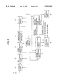
- FIG. 1 illustrates the configuration of a spectrum spread receiver according to a first embodiment of the present invention.
- reference numeral 1 designates an antenna; 2, a receiving circuit; 3, an A/D converter circuit; 4, a first despreading circuit; 5, a delay profile measurement instrument; 6, a searcher circuit; 7, a second despreading circuit; 8, a timing control circuit; 9, a demodulation circuit; 10, a delayed waveform phase determination circuit; and 11, a received data conversion circuit.
- a signal received by the antenna 1 is amplified by the receiving circuit 2, and the thus-amplified signal is subjected to analog-to-digital conversion by the A/D conversion circuit 3.
- the thus-converted digital signal is subjected to detection of correlation by the first despreading circuit 4, and the delay profile measurement instrument 5 averages the received signal.
- the searcher circuit 6 selects a delayed waveform of several higher-level samples having a high receiving level and outputs the thus-selected waveform to the second despreading circuit 7 and the delayed waveform phase determination circuit 10.
- the second despreading circuit 7 despreads the digital data signal converted by the A/D converter circuit 3 to thereby obtain received data.
- the delayed waveform determination circuit 10 determines whether or not the delayed waveform detected by the searcher circuit 6 is in the same phase as the previously detected delayed waveform and outputs a delayed waveform switch signal a. If the waveforms are out of phase with each other, the delayed waveform switch signal a is turned on.
- the demodulation circuit 9 respectively demodulates the first half and second half of the received signal as a boundary is a received signal at which a delayed waveform switch signal a is turned on by use of the phase estimated from a first known signal and the phase estimated from a second known signal, without interpolating the phase estimated from the first and second known signals included in both ends of the information signal.
- the thus-demodulated delayed waveforms are subjected to RAKE synthesis.
- the demodulation circuit 9 demodulates the received signal by interpolating the phase estimated from the first and second known signals included in both ends of the received signal, and the thus-demodulated delayed waveforms are subjected to RAKE synthesis.
- the received data conversion circuit 11 obtains desired information by dividing thus-composed data into a control signal and a sound signal or data.
- the timing control circuit 8 controls all timing and sequences of the spectrum spread receiver.
- FIG. 2 illustrates the configuration of the demodulation circuit 9 of the first embodiment.
- the elements numbered from 12 to 20 provided in FIG. 2 are identical with those numbered from 112 to 120 of the conventional detection circuit provided in FIG. 9. During the periods of the known signals, they operate in the same way as do the elements of the conventional circuit provided in FIG. 9.
- a switch 20 is in the OFF state during the period of an information signal.
- the phase of the received signal is not updated by phase update sections 24.
- Multipliers 16 assign optimum weights 22 estimated during the period of a first known signal 14 to the first half of the received signal in relation to the point in time at which the delayed waveform switch signal a is turned on.
- the multipliers 16 assign the optimum weights 22 estimated during the period of a second known signal 15 to the second half of the received signal.
- a switch 25 effects the switching between known signals 14 and 15.
- An adder 17 adds up delayed waveforms of the received signal.
- An identifier 18 determines whether an output of the adder 17 is positive or negative, thereby reproducing the data 19 with fewer errors. Error signals 21 are calculated by the adders 26 through addition of the first known signal 14 or second known signal 15 to the outputs of the multipliers 16.
- the delayed waveform which the delayed waveform switch signal a is turned off is subjected to primary interpolation of the weighting coefficients 22 estimated from the error signals 21 at a phase update section 24 by using the Equation (1), is updated the weighting coefficients 22, and then is assigned the optimum weight.
- the adder 17 adds up thus-weighted delayed waveforms.
- the identifier 18 determines whether an output of the adder 17 is positive or negative, thereby reproducing the data 19 with fewer errors.
- FIG. 3 illustrates an example of operation of the demodulation circuit 9.
- the delayed waveforms (1) and (3) can be demodulated by interpolating the known signals tr1 and tr2.
- the delayed waveform (2) to be demodulated is switched to the delayed waveform (4), it is necessary to demodulate the delayed waveform (2) in order to obtain the first half of the received signal in relation to the delayed waveform switch signal a.
- the delayed waveforms (2) and (4) are subjected to fading independently of each other, and therefore the received signal is degraded by interpolation of the known signals tr1 and tr2.
- the first half of the received signal is obtained by demodulating the delayed waveform (2) by use of the known signal tr1
- the second half of the received signal is obtained by demodulating the delayed waveform (4) by use of the known signal tr2.
- the spectrum spread receiver is provided with the delayed waveform phase determination circuit 10. Accordingly, even if the phase of the delayed waveform to be demodulated is switched, the received signal can be prevented from becoming degraded.
- FIG. 4 illustrates the configuration of the demodulation circuit of the second embodiment.
- the elements numbered from 31 to 38 provided in FIG. 4 are the same as those numbered from 112 to 119 of the conventional circuitry illustrated in FIG. 9. During the periods of the known signals, they operate in the same way as do the elements of the conventional circuit provided in FIG. 9. Even in the period of the information signal, weighting coefficients 40 are updated.
- the first half of the received signal before the delayed waveform which the delayed waveform switch signal a becomes in the ON state updates the weighting coefficient 40 of the multiplier 35 so that the weighting coefficient 40 estimated in the period of the first known signal 33 minimizes the square of the sum of error signals 39 (differences between the outputs of the multipliers 35 and the result of the addition of the output of the identifier 37 carried out by the adder 45) for each delayed waveform by using an adaptive algorithm (an RLS algorithm or the like) in the phase update section 42 even in the period of the information signal.
- an adaptive algorithm an RLS algorithm or the like
- the multipliers 35 assign the thus-updated optimum weights 40 to the delayed waveforms.
- An adder 36 adds up the thus-weighted delayed waveforms.
- the identifier 37 determines whether an output of the adder 36 is positive or negative, thereby reproducing data 38 with fewer errors.
- operations are performed on the basis of the weighting coefficients 40 estimated from the second known signal 34 in the same way as for the first half of the received signal.
- the period of the signal between the first and second know signals 33 and 34 is equally divided.
- the first half of the received signal updates the weighting coefficient 40 estimated in the period of the first known signal 33 of the multiplier 35 so that the weighting coefficient 40 estimated in the period of the first known signal 33 minimizes the square of the sum of error signals 39 (differences between the outputs of the multipliers 35 and the output of the identifier 37) for each delayed waveform by using an adaptive algorithm (an RLS algorithm or the like) in the phase update section 42.
- the multipliers 35 assign thus-updated optimum weights 40 to the delayed waveforms.
- the adder 36 adds up the thus-weighted waveforms.
- the identifier 37 determines the output of the adder 36 to be positive or negative, thereby reproducing the data 38 with fewer errors.
- operations are performed on the basis of the weighting coefficients 40 estimated from the second known signal 34 in the same way as in the case of demodulation of the first half of the received signal.
- the spectrum spread receiver is provided with the delayed waveform phase determination circuit 10 so that the demodulation circuit 9 can sequentially update the phases of the delayed waveforms.
- the quality of a received signal can be improved, and the received signal can be prevented from becoming degraded even if the phase of the delayed waveform to be demodulated is switched to another phase.
- FIG. 5 illustrates the configuration of a spectrum spread receiver according to a third embodiment of the present invention.
- reference numeral 51 designates an antenna; 52, a receiving circuit; 53, an A/D conversion circuit; 54, a first despreading circuit; 55, a delay profile measurement instrument; 56, a searcher circuit; 57, a second despreading circuit; 58, a timing control circuit; 59, a demodulation circuit; 60, a delayed waveform phase determination circuit; 61, a received data conversion circuit; and 62, a fading estimation circuit.
- a signal received by the antenna 51 is amplified by the receiving circuit 52, and the thus-amplified signal is subjected to analog-to-digital conversion by the A/D conversion circuit 53.
- the first despreading circuit 54 detects correlation, and the delay profile measurement instrument 55 averages the received signal.
- the searcher circuit 56 selects several higher-level sampled delayed waveforms having a high receiving level and outputs the thus-selected delayed waveforms to the second despreading circuit 57 and the delayed waveform phase determination circuit 60.
- the second despreading circuit 57 despreads the digital data signal converted by the A/D conversion circuit 53 to thereby obtain received data.
- the delayed waveform phase determination circuit 60 determines whether or not the delayed waveform detected by the searcher circuit 56 is in the same phase as the previously detected delayed waveform. If they are out of phase with each other, an ON/OFF signal is output to turn on the delayed waveform switch signal a.
- the fading estimation circuit 62 detects variations in the level of a signal output from the delay profile measurement instrument 55, whereby a fading pitch b is calculated from the amount of variations.
- the demodulation circuit 59 respectively demodulates the first half and second half of the received signal, as a boundary is a received signal at which a delayed waveform switch signal a is turned on, by use of the phase estimated from the first known signal and the phase estimated from the second known signal, without interpolating the phases estimated from the first and second known signals included in both ends of the information signal.
- the thus-demodulated delayed waveforms are subjected to RAKE synthesis.
- the demodulation circuit 59 respectively demodulates the first half and second half of the received signal, as a boundary is a received signal a at which a delayed waveform switch signal is turned on, by use of the phase that is estimated from the first known signal and then is sequentially updated by an adaptive algorithm or the like, as well as the phase that is estimated from the second known signal and then, is sequentially updated by an adaptive algorithm or the like.
- the thus-demodulated delayed waveforms are subjected to RAKE synthesis.
- the delayed waveform switch signal a is in the OFF state, it is determined whether the phase is interpolated according to the fading pitch b detected by the fading estimation circuit 62 or the phase is sequentially updated.
- required operations are the same as those required in the first embodiment.
- sequential updating of the phase required operations are the same as those required in the second embodiment.
- the received data conversion circuit 61 obtains desired information by dividing the received data into a control signal and an audio signal or data.
- the timing control circuit 58 controls all timing and sequences of the spectrum spread receiver.
- FIG. 6 illustrates the configuration of the demodulation circuit 59 of the third embodiment.
- the elements numbered from 71 to 78 provided in FIG. 6 are identical with those numbered from 112 to 119 of the conventional detection circuit provided in FIG. 9.
- the switches 83 are turned on or off. If the fading pitch b is slower than the cycle of interpolation of the first and second known signals 73 and 74, the switches 83 is turned off. In contrast, if the fading pitch b is faster than the cycle of interpolation of the first and second known signals 73 and 74, the switches 83 is turned on.
- the first half of the received signal before the delayed waveform which the delayed waveform switch signal a becomes in the ON state updates the weighting coefficient 80 of the multiplier 75 so that the weighting coefficient 80 estimated in the period of the first known signal 73 minimizes the square of the sum of error signals 79 (differences between the outputs of the multipliers 75 and the result of the addition of the output of the identifier 77 carried out by the adder 86) for each delayed waveform by using an adaptive algorithm (an RLS algorithm or the like) in the phase update section 82 even in the period of the information signal.
- an adaptive algorithm an RLS algorithm or the like
- the amplifiers 75 assign the thus-updated optimum weighting coefficients 80 to the delayed waveforms.
- An adder 76 adds up the thus-weighted delayed waveforms.
- the identifier 77 determines whether an output of the adder 76 is positive or negative, thereby reproducing data 78 with fewer errors.
- the second half of the received signal updates the weighting coefficient 80 of the multiplier 75 so that the weighting coefficient 80 estimated in the period of the second known signal 73 minimizes the square of the sum of error signals 79 (differences between the outputs of the multipliers 75 and the output of the identifier 77) for each delayed waveform by using an adaptive algorithm (an RLS algorithm or the like) in the phase update section 82 even in the period of the information signal.
- an adaptive algorithm an RLS algorithm or the like
- the amplifiers 75 assign the thus-updated optimum weighting coefficients 80 to the delayed waveforms.
- the adder 76 adds up the thus-weighted delayed waveforms.
- the identifier 77 determines whether the output of the adder 76 is positive or negative, thereby reproducing the data 78 with fewer errors.
- delayed waveform switch signal a is in the ON state and the switches 83 are in the OFF state, required operations are the same as those carried out in the case of the first embodiment where the delayed waveform switch signal a is in the ON state.
- delayed waveform switch signal a and the switches 83 are in the OFF state, required operations are the same as those carried out in the case of the second embodiment where the delayed waveform switch signal a is in the OFF state.
- the spectrum spread receiver is provided with the delayed waveform determination circuit 60 and the fading estimation circuit 62.
- the fading estimation circuit 62 estimates the fading pitch b. Provided that the fading pitch is slower than the cycle of interpolation of the known signals, it is possible to reduce the amount of electric current consumed by the receiver by selecting interpolation synchronization detection as a phase estimation method. In contrast, provided that the fading pitch b is faster than the cycle of interpolation of the known signals, the followability of the receiver with respect to high-speed fading can be improved, thereby improving the quality of the received signal. Even if the phase of a delayed waveform to be demodulated is switched to another phase, the received signal is prevented from becoming degraded.
- a spectrum spread receiver of the fourth embodiment is the same in configuration as that which is provided in FIG. 5 except the configuration and operation of the demodulation circuit 59.
- FIG. 7 illustrates the configuration of the demodulation circuit of the fourth embodiment.
- phase estimation sections 104 estimate transmission paths which are in a varying state due to multipath Reyleigh fading for respective delayed waveforms according to an adaptive algorithm (e.g., an RLS algorithm or the like).
- the demodulation circuit controls weighting coefficients 103 of amplifiers 98 so as to minimize the square of the sum of errors 102 (the differences between outputs of the amplifiers 98 and the first known signal 93 or second known signal 94 obtained through adding operations carried out by adders 110).
- weighting coefficients 103 of amplifiers 98 so as to minimize the square of the sum of errors 102 (the differences between outputs of the amplifiers 98 and the first known signal 93 or second known signal 94 obtained through adding operations carried out by adders 110).
- a third or four known signal 95 is then defined by the first or second known signals 93 and 94 as well as from the thus-demodulated signal. Then, the switch 97 is turned off.
- the phase estimation sections 104 again estimate transmission paths which is in a varying state due to multipath Reyleigh fading for respective delayed waveforms according to an adaptive algorithm (e.g., an RLS algorithm or the like).
- an adaptive algorithm e.g., an RLS algorithm or the like.
- the demodulation circuit controls the weighting coefficients 103 of the multipliers 98 so as to minimize the errors 102 (the differences between the outputs of the multipliers 98 and the third known signal 95 or fourth known signal 96 obtained through adding operations carried out by the adders 110).
- a fading pitch b it is determined according to a fading pitch b whether switches 106 are turned on or off. If the fading pitch b is slower than the cycle of interpolation of the known signals 93 and 94, the switches 106 are turned off. In contrast, if the fading pitch b is faster than the cycle of interpolation of the first and second known signals 93 and 94, the switches 106 are turned on.
- the first half of the received signal before the delayed waveform which the delayed waveform switch signal a becomes in the ON state updates the weighting coefficient 103 of the multiplier 98 so that the weighting coefficient 103 estimated in the period of the third known signal 95 minimizes the square of the sum of error signals 102 (differences between the outputs of the multipliers 98 and the output of the identifier 100) for each delayed waveform by using an adaptive algorithm (an RLS algorithm or the like) in the phase update section 105 even in the period of the information signal.
- the multipliers 98 assign the thus-updated optimum weighting coefficients to the delayed waveforms.
- An adder 99 adds up the thus-weighted delayed waveforms.
- the identifier 100 determines whether an output of the adder 99 is positive or negative, thereby reproducing data 101 with fewer errors.
- the second half of the received signal before the delayed waveform which the delayed waveform switch signal a becomes in the ON state updates the weighting coefficient 103 of the multiplier 98 so that the weighting coefficient 103 estimated in the period of the fourth known signal 96 minimizes the square of the sum of error signals 102 (differences between the outputs of the multipliers 98 and the output of the identifier 100) for each delayed waveform by using an adaptive algorithm (an RLS algorithm or the like) in the phase update section 105 even in the period of the information signal.
- an adaptive algorithm an RLS algorithm or the like
- the multipliers 98 assign the thus-updated optimum weighting coefficients 103 to the delayed waveforms.
- the adder 99 adds up the thus-weighted delayed waveforms.
- the identifier 100 determines whether the output of the adder 99 is positive or negative, thereby reproducing the data 101 with fewer errors.
- the first half received signal of the received signal of the delayed waveform in which the delayed waveform switch signal a is in ON state updates the weighting coefficient 103 of the multiplier 98 so that the weighting coefficient 103 estimated during the period of the third known signal 95 minimizes the square of the sum of the error 102 (differences between the outputs of the multiplier 98 and the output of the identifier 100) for each delay waveform by using an adaptive algorithm (RLS algorithm or the like) in the phase update section 105.
- the multipliers 98 assign the thus-updated optimum weighting coefficients to the delayed waveforms.
- the adder 99 adds up the thus-weighted delayed waveforms.
- the identifier 100 determines whether the output of the adder 99 is positive or negative, thereby reproducing data 101 with fewer errors.
- the second half received signal of the received signal of the delayed waveform in which the delayed waveform switch signal a is in ON state updates the weighting coefficient 103 of the multiplier 98 so that the weighting coefficient 103 estimated during the period of the fourth known signal 96 minimizes the square of the sum of the error 102 (differences between the outputs of the multiplier 98 and the output of the identifier 100) for each delay waveform by using an adaptive algorithm (RLS algorithm or the like) in the phase update section 105.
- the amplifiers 98 assign the thus-updated optimum weighting coefficients 103 to the delayed waveforms.
- the adder 99 adds up the thus-weighted delayed waveforms.
- the identifier 100 determines whether the output of the adder 99 is positive or negative, thereby reproducing the data 101 with fewer errors.
- the delay waveform switch signal a is in the OFF state, the period of the signal between the known signals is equally divided.
- the first half received signal updates the weighting coefficient 103 of the multiplier 98 so that the weighting coefficient 103 estimated during the period of the third known signal 95 minimizes the square of the sum of the error 102 (differences between the outputs of the multiplier 98 and the output of the identifier 100) for each delay waveform by using an adaptive algorithm (RLS algorithm or the like) in the phase update section 105 even in the period of the information signal.
- the multipliers 98 assign the thus-updated optimum weighting coefficients to the delayed waveforms.
- the adder 99 adds up the thus-weighted delayed waveforms.
- the identifier 100 determines whether the output of the adder 99 is positive or negative, thereby reproducing data 101 with fewer errors.
- the second half received signal updates the weighting coefficient 103 of the multiplier 98 so that the weighting coefficient 103 estimated during the period of the fourth known signal 96 minimizes the square of the sum of the error 102 (differences between the outputs of the multiplier 98 and the output of the identifier 100) for each delay waveform by using an adaptive algorithm (RLS algorithm or the like) in the phase update section 105 even in the period of the information signal.
- the multipliers 98 assign the thus-updated optimum weighting coefficients 103 to the delayed waveforms.
- the adder 99 adds up the thus-weighted delayed waveforms.
- the identifier 100 determines whether the output of the adder 99 is positive or negative, thereby reproducing the data 101 with fewer errors.
- the weighting coefficients 103 estimated by the third and fourth known signals 95 and 96 are subjected to the primary interpolation performed by the phase update sections 105 by use of Formula (1), thereby updating the weighting coefficients 103.
- the multipliers 98 assign the thus-updated optimum weighting coefficients 103 to the delayed waveforms.
- the adder 99 adds up the thus-weighted delayed waveforms.
- the identifier 100 determines whether the output of the adder 99 is positive or negative, thereby reproducing the data 101 with fewer errors.
- the spectrum spread receiver is provided with the delayed waveform determination circuit 60 and the fading estimation circuit 62.
- the fading estimation circuit 62 estimates the fading pitch b. If the fading pitch is slower than the cycle of interpolation of the known signals, it is possible to reduce the amount of electric current consumed by the receiver by selecting interpolation synchronization detection as a phase estimation method. In contrast, if the fading pitch b is faster than the cycle of interpolation of the known signals, the followability of the receiver with respect to high-speed fading can be improved, thereby improving the quality of a received signal. Further, the phase of the delayed waveform is estimated again by use of the known signals and the demodulated signal, which enables accurate estimation of the phase. As a result, quality of receipt of a signal can be improved. Even if the phase of a delayed waveform to be demodulated is switched to another phase, it is possible to prevent receipt of the signal from becoming degraded.
- a spectrum spread communication receiving apparatus is provided with a delayed waveform phase determination circuit which determines whether or not a delayed waveform is in the same phase as the previously detected delayed waveform, and which outputs a delayed waveform changeover ON/OFF signal if they are out of phase with each other. Further, the communications apparatus is provided with a demodulation circuit.
- the demodulation circuit respectively demodulates the first half and second half of the received signal in relation to the point in time at which the delayed waveform switch signal is turned on, by use of the phase estimated from a first known signal and the phase estimated from a second known signal, without interpolating phases estimated from the first and second known signals included in both ends of the received signal for pilot coherent detection scheme with interpolation purposes.
- the phase of the delayed waveform is switched to another phase, the received signal will be prevented from becoming degraded.
Abstract
Description
Z(k)=Z.sub.1 (N-k)/N+Z.sub.2 k/N (1)
Claims (4)
Applications Claiming Priority (2)
| Application Number | Priority Date | Filing Date | Title |
|---|---|---|---|
| JP8-076428 | 1996-03-29 | ||
| JP7642896A JP3310160B2 (en) | 1996-03-29 | 1996-03-29 | Spread spectrum receiver |
Publications (1)
| Publication Number | Publication Date |
|---|---|
| US5822364A true US5822364A (en) | 1998-10-13 |
Family
ID=13604907
Family Applications (1)
| Application Number | Title | Priority Date | Filing Date |
|---|---|---|---|
| US08/824,833 Expired - Lifetime US5822364A (en) | 1996-03-29 | 1997-03-26 | Receiving apparatus for spectrum spread system |
Country Status (6)
| Country | Link |
|---|---|
| US (1) | US5822364A (en) |
| EP (1) | EP0798870B1 (en) |
| JP (1) | JP3310160B2 (en) |
| KR (1) | KR100370590B1 (en) |
| CN (1) | CN1115029C (en) |
| DE (1) | DE69726786T2 (en) |
Cited By (12)
| Publication number | Priority date | Publication date | Assignee | Title |
|---|---|---|---|---|
| US5978411A (en) * | 1996-03-22 | 1999-11-02 | Matsushita Electric Industrial Co., Ltd. | Synchronizer for receiver of spread spectrum communication apparatus |
| US6081549A (en) * | 1997-01-10 | 2000-06-27 | Yozan Inc. | Phase correction method and apparatus for spectrum spread wireless communication receiver |
| WO2002011309A1 (en) * | 2000-07-31 | 2002-02-07 | Morphics Technology, Inc. | Generic finger architecture for spread spectrum applications |
| US6556619B2 (en) * | 2000-09-05 | 2003-04-29 | Nec Corporation | Frequency adjusting circuit in code division multiple access communication system |
| US20030123408A1 (en) * | 2001-12-28 | 2003-07-03 | Naoyuki Saitou | CDMA receiving apparatus |
| US20030137996A1 (en) * | 2001-12-14 | 2003-07-24 | Mark Roh | Acquisition of a gated pilot signal |
| US6757345B1 (en) * | 1998-12-31 | 2004-06-29 | Nokia Networks Oy | Reception method and receiver |
| US20050083995A1 (en) * | 2003-09-26 | 2005-04-21 | Fujitsu Ten Limited | Radar apparatus |
| US6912259B1 (en) * | 1998-09-03 | 2005-06-28 | Nec Corporation | Interpolation synchronous detection method and radio communication system |
| US7042862B1 (en) * | 1999-07-21 | 2006-05-09 | Nec Corporation | Path searching method and device |
| US20090267269A1 (en) * | 2008-04-25 | 2009-10-29 | Jin Hong Lim | Selective Deposition Modeling Using CW UV LED Curing |
| US20180219575A1 (en) * | 2017-01-27 | 2018-08-02 | Lapis Semiconductor Co., Ltd. | Signal detection circuit and signal detection method |
Families Citing this family (7)
| Publication number | Priority date | Publication date | Assignee | Title |
|---|---|---|---|---|
| JP2000252960A (en) * | 1999-03-01 | 2000-09-14 | Toshiba Corp | Rake reception device |
| JP2000307469A (en) * | 1999-04-16 | 2000-11-02 | Matsushita Electric Ind Co Ltd | Device and method for spread spectrum receiver |
| EP1069696B1 (en) | 1999-06-24 | 2006-09-27 | Alcatel | Receiver and method with enhanced performance for CDMA transmission |
| JP3884896B2 (en) | 2000-04-06 | 2007-02-21 | 株式会社エヌ・ティ・ティ・ドコモ | Communication quality acquisition apparatus and communication quality acquisition method |
| EP1154584A1 (en) * | 2000-05-12 | 2001-11-14 | Siemens Aktiengesellschaft | Mobile station and method for allocating rake fingers and tracking devices |
| EP1605619A4 (en) * | 2003-02-28 | 2012-01-11 | Ntt Docomo Inc | Radio communication system and radio communication method |
| TWI324469B (en) * | 2006-01-13 | 2010-05-01 | Via Tech Inc | Method and apparatus for delaying sampled signal |
Citations (12)
| Publication number | Priority date | Publication date | Assignee | Title |
|---|---|---|---|---|
| US5105437A (en) * | 1990-07-26 | 1992-04-14 | Unisys Corporation | Programmable digital acquisition and tracking controller |
| US5150384A (en) * | 1990-09-28 | 1992-09-22 | Motorola, Inc. | Carrier recovery method and apparatus having an adjustable response time determined by carrier signal parameters |
| US5283780A (en) * | 1990-10-18 | 1994-02-01 | Stanford Telecommunications, Inc. | Digital audio broadcasting system |
| US5361276A (en) * | 1993-09-13 | 1994-11-01 | At&T Bell Laboratories | All digital maximum likelihood based spread spectrum receiver |
| US5425058A (en) * | 1993-07-28 | 1995-06-13 | Martin Marietta Corporation | MSK phase acquisition and tracking method |
| US5448600A (en) * | 1993-08-13 | 1995-09-05 | Matra Communication | Method for selecting propagation paths retained for receiving messages transmitted by CDMA radiocommunication |
| US5619524A (en) * | 1994-10-04 | 1997-04-08 | Motorola, Inc. | Method and apparatus for coherent communication reception in a spread-spectrum communication system |
| US5659573A (en) * | 1994-10-04 | 1997-08-19 | Motorola, Inc. | Method and apparatus for coherent reception in a spread-spectrum receiver |
| US5692006A (en) * | 1995-07-31 | 1997-11-25 | Qualcomm Incorporated | Adaptive despreader |
| US5691974A (en) * | 1995-01-04 | 1997-11-25 | Qualcomm Incorporated | Method and apparatus for using full spectrum transmitted power in a spread spectrum communication system for tracking individual recipient phase, time and energy |
| US5737327A (en) * | 1996-03-29 | 1998-04-07 | Motorola, Inc. | Method and apparatus for demodulation and power control bit detection in a spread spectrum communication system |
| US5742637A (en) * | 1996-08-20 | 1998-04-21 | Golden Bridge Technology, Inc. | Fast phase estimation in digital communication systems |
Family Cites Families (2)
| Publication number | Priority date | Publication date | Assignee | Title |
|---|---|---|---|---|
| US5263026A (en) * | 1991-06-27 | 1993-11-16 | Hughes Aircraft Company | Maximum likelihood sequence estimation based equalization within a mobile digital cellular receiver |
| WO1995035615A1 (en) * | 1994-06-22 | 1995-12-28 | Ntt Mobile Communications Network Inc. | Synchronous detector and synchronizing method for digital communication receiver |
-
1996
- 1996-03-29 JP JP7642896A patent/JP3310160B2/en not_active Expired - Lifetime
-
1997
- 1997-03-26 DE DE1997626786 patent/DE69726786T2/en not_active Expired - Lifetime
- 1997-03-26 US US08/824,833 patent/US5822364A/en not_active Expired - Lifetime
- 1997-03-26 EP EP19970105113 patent/EP0798870B1/en not_active Expired - Lifetime
- 1997-03-28 KR KR1019970011224A patent/KR100370590B1/en not_active IP Right Cessation
- 1997-03-29 CN CN97109692A patent/CN1115029C/en not_active Expired - Lifetime
Patent Citations (12)
| Publication number | Priority date | Publication date | Assignee | Title |
|---|---|---|---|---|
| US5105437A (en) * | 1990-07-26 | 1992-04-14 | Unisys Corporation | Programmable digital acquisition and tracking controller |
| US5150384A (en) * | 1990-09-28 | 1992-09-22 | Motorola, Inc. | Carrier recovery method and apparatus having an adjustable response time determined by carrier signal parameters |
| US5283780A (en) * | 1990-10-18 | 1994-02-01 | Stanford Telecommunications, Inc. | Digital audio broadcasting system |
| US5425058A (en) * | 1993-07-28 | 1995-06-13 | Martin Marietta Corporation | MSK phase acquisition and tracking method |
| US5448600A (en) * | 1993-08-13 | 1995-09-05 | Matra Communication | Method for selecting propagation paths retained for receiving messages transmitted by CDMA radiocommunication |
| US5361276A (en) * | 1993-09-13 | 1994-11-01 | At&T Bell Laboratories | All digital maximum likelihood based spread spectrum receiver |
| US5619524A (en) * | 1994-10-04 | 1997-04-08 | Motorola, Inc. | Method and apparatus for coherent communication reception in a spread-spectrum communication system |
| US5659573A (en) * | 1994-10-04 | 1997-08-19 | Motorola, Inc. | Method and apparatus for coherent reception in a spread-spectrum receiver |
| US5691974A (en) * | 1995-01-04 | 1997-11-25 | Qualcomm Incorporated | Method and apparatus for using full spectrum transmitted power in a spread spectrum communication system for tracking individual recipient phase, time and energy |
| US5692006A (en) * | 1995-07-31 | 1997-11-25 | Qualcomm Incorporated | Adaptive despreader |
| US5737327A (en) * | 1996-03-29 | 1998-04-07 | Motorola, Inc. | Method and apparatus for demodulation and power control bit detection in a spread spectrum communication system |
| US5742637A (en) * | 1996-08-20 | 1998-04-21 | Golden Bridge Technology, Inc. | Fast phase estimation in digital communication systems |
Non-Patent Citations (2)
| Title |
|---|
| Technical Report of IEICE, A P94 74, RCS94 98 (1994 10), Performance of Coherent RAKE Detection using Interpolation on DS/CDMA , Akihiro Higashi et al. * |
| Technical Report of IEICE, A-P94-74, RCS94-98 (1994-10), "Performance of Coherent RAKE Detection using Interpolation on DS/CDMA", Akihiro Higashi et al. |
Cited By (16)
| Publication number | Priority date | Publication date | Assignee | Title |
|---|---|---|---|---|
| US5978411A (en) * | 1996-03-22 | 1999-11-02 | Matsushita Electric Industrial Co., Ltd. | Synchronizer for receiver of spread spectrum communication apparatus |
| US6081549A (en) * | 1997-01-10 | 2000-06-27 | Yozan Inc. | Phase correction method and apparatus for spectrum spread wireless communication receiver |
| US6912259B1 (en) * | 1998-09-03 | 2005-06-28 | Nec Corporation | Interpolation synchronous detection method and radio communication system |
| US6757345B1 (en) * | 1998-12-31 | 2004-06-29 | Nokia Networks Oy | Reception method and receiver |
| US7042862B1 (en) * | 1999-07-21 | 2006-05-09 | Nec Corporation | Path searching method and device |
| WO2002011309A1 (en) * | 2000-07-31 | 2002-02-07 | Morphics Technology, Inc. | Generic finger architecture for spread spectrum applications |
| US6556619B2 (en) * | 2000-09-05 | 2003-04-29 | Nec Corporation | Frequency adjusting circuit in code division multiple access communication system |
| AU774123B2 (en) * | 2000-09-05 | 2004-06-17 | Nec Corporation | Code division multiple access communication system |
| US7586837B2 (en) * | 2001-12-14 | 2009-09-08 | Qualcomm Incorporated | Acquisition of a gated pilot signal |
| US20030137996A1 (en) * | 2001-12-14 | 2003-07-24 | Mark Roh | Acquisition of a gated pilot signal |
| US20030123408A1 (en) * | 2001-12-28 | 2003-07-03 | Naoyuki Saitou | CDMA receiving apparatus |
| US20050083995A1 (en) * | 2003-09-26 | 2005-04-21 | Fujitsu Ten Limited | Radar apparatus |
| US7724802B2 (en) * | 2003-09-26 | 2010-05-25 | Fujitsu Ten Limited | Radar apparatus |
| US20090267269A1 (en) * | 2008-04-25 | 2009-10-29 | Jin Hong Lim | Selective Deposition Modeling Using CW UV LED Curing |
| US20180219575A1 (en) * | 2017-01-27 | 2018-08-02 | Lapis Semiconductor Co., Ltd. | Signal detection circuit and signal detection method |
| US10333583B2 (en) * | 2017-01-27 | 2019-06-25 | Lapis Semiconductor Co., Ltd. | Signal detection circuit and signal detection method |
Also Published As
| Publication number | Publication date |
|---|---|
| CN1164784A (en) | 1997-11-12 |
| EP0798870A2 (en) | 1997-10-01 |
| JP3310160B2 (en) | 2002-07-29 |
| KR970068221A (en) | 1997-10-13 |
| KR100370590B1 (en) | 2003-04-11 |
| CN1115029C (en) | 2003-07-16 |
| EP0798870A3 (en) | 1999-10-20 |
| JPH09270734A (en) | 1997-10-14 |
| DE69726786D1 (en) | 2004-01-29 |
| EP0798870B1 (en) | 2003-12-17 |
| DE69726786T2 (en) | 2004-10-07 |
Similar Documents
| Publication | Publication Date | Title |
|---|---|---|
| US5822364A (en) | Receiving apparatus for spectrum spread system | |
| US7336598B2 (en) | Guard interval length control method in OFDM system and OFDM transmitting and receiving apparatuses | |
| JP3913879B2 (en) | Communication control apparatus and method based on moving speed | |
| US7106784B2 (en) | Universal rake receiver | |
| US5706314A (en) | Joint maximum likelihood channel and timing error estimation | |
| US20070248191A1 (en) | Baseband sample selection | |
| KR100362030B1 (en) | Reception path search method and searcher circuit of cdma reception device | |
| CA2112151C (en) | Digital data demodulating apparatus | |
| JP4720658B2 (en) | Synchronization detection circuit and multi-mode wireless communication device | |
| EP1138136A1 (en) | Synchronization tracking method | |
| WO2007135400A1 (en) | Refinement of channel estimation with a bank of filters | |
| CA2035774C (en) | Frame phase estimation method and circuit | |
| KR100307004B1 (en) | Interpolation synchronous detection method and radio communication system | |
| US6990160B1 (en) | Reception apparatus and method | |
| US6014405A (en) | Spread spectrum multipath receiver without a tracking loop | |
| KR100504360B1 (en) | Receiver and reception method | |
| JP2001189768A (en) | Synchronous demodulator | |
| EP1119919A1 (en) | Method for selecting modulation detector in receiver, and receiver | |
| JP2000091973A (en) | Rake synthesis circuit | |
| JP3816684B2 (en) | Spread spectrum receiver | |
| JPH10112673A (en) | Rake reception method and receiver therefor | |
| EP1089476A1 (en) | Spread spectrum receiver and method of receiving signals | |
| JP3314809B2 (en) | Frequency offset compensation circuit | |
| JP3990829B2 (en) | Data demodulator | |
| EP1128595A2 (en) | Synchronisation of a radio reception apparatus |
Legal Events
| Date | Code | Title | Description |
|---|---|---|---|
| AS | Assignment |
Owner name: MATSUSHITA ELECTRIC INDUSTRIAL CO., LTD., JAPAN Free format text: ASSIGNMENT OF ASSIGNORS INTEREST;ASSIGNORS:YAMADA, DAISUKE;TAKAKUSAKI, KEIJI;REEL/FRAME:008498/0557 Effective date: 19970321 |
|
| STCF | Information on status: patent grant |
Free format text: PATENTED CASE |
|
| FEPP | Fee payment procedure |
Free format text: PAYOR NUMBER ASSIGNED (ORIGINAL EVENT CODE: ASPN); ENTITY STATUS OF PATENT OWNER: LARGE ENTITY |
|
| FPAY | Fee payment |
Year of fee payment: 4 |
|
| FPAY | Fee payment |
Year of fee payment: 8 |
|
| FPAY | Fee payment |
Year of fee payment: 12 |
|
| FEPP | Fee payment procedure |
Free format text: PAYER NUMBER DE-ASSIGNED (ORIGINAL EVENT CODE: RMPN); ENTITY STATUS OF PATENT OWNER: LARGE ENTITY Free format text: PAYOR NUMBER ASSIGNED (ORIGINAL EVENT CODE: ASPN); ENTITY STATUS OF PATENT OWNER: LARGE ENTITY |
|
| AS | Assignment |
Owner name: PANASONIC CORPORATION, JAPAN Free format text: CHANGE OF NAME;ASSIGNOR:MATSUSHITA ELECTRIC INDUSTRIAL CO., LTD.;REEL/FRAME:031814/0732 Effective date: 20081001 |
|
| AS | Assignment |
Owner name: HIGHBRIDGE PRINCIPAL STRATEGIES, LLC, AS COLLATERA Free format text: LIEN;ASSIGNOR:OPTIS WIRELESS TECHNOLOGY, LLC;REEL/FRAME:032180/0115 Effective date: 20140116 |
|
| AS | Assignment |
Owner name: OPTIS WIRELESS TECHNOLOGY, LLC, TEXAS Free format text: ASSIGNMENT OF ASSIGNORS INTEREST;ASSIGNOR:PANASONIC CORPORATION;REEL/FRAME:032326/0707 Effective date: 20140116 |
|
| AS | Assignment |
Owner name: WILMINGTON TRUST, NATIONAL ASSOCIATION, MINNESOTA Free format text: SECURITY INTEREST;ASSIGNOR:OPTIS WIRELESS TECHNOLOGY, LLC;REEL/FRAME:032437/0638 Effective date: 20140116 |
|
| AS | Assignment |
Owner name: OPTIS WIRELESS TECHNOLOGY, LLC, TEXAS Free format text: RELEASE BY SECURED PARTY;ASSIGNOR:HPS INVESTMENT PARTNERS, LLC;REEL/FRAME:039361/0001 Effective date: 20160711 |