US5822855A - Method of making electrical connector having a two part articulated housing - Google Patents
Method of making electrical connector having a two part articulated housing Download PDFInfo
- Publication number
- US5822855A US5822855A US08/620,375 US62037596A US5822855A US 5822855 A US5822855 A US 5822855A US 62037596 A US62037596 A US 62037596A US 5822855 A US5822855 A US 5822855A
- Authority
- US
- United States
- Prior art keywords
- connector
- housing
- circuit board
- housing parts
- strip
- Prior art date
- Legal status (The legal status is an assumption and is not a legal conclusion. Google has not performed a legal analysis and makes no representation as to the accuracy of the status listed.)
- Expired - Fee Related
Links
Images


Classifications
-
- H—ELECTRICITY
- H01—ELECTRIC ELEMENTS
- H01R—ELECTRICALLY-CONDUCTIVE CONNECTIONS; STRUCTURAL ASSOCIATIONS OF A PLURALITY OF MUTUALLY-INSULATED ELECTRICAL CONNECTING ELEMENTS; COUPLING DEVICES; CURRENT COLLECTORS
- H01R12/00—Structural associations of a plurality of mutually-insulated electrical connecting elements, specially adapted for printed circuits, e.g. printed circuit boards [PCB], flat or ribbon cables, or like generally planar structures, e.g. terminal strips, terminal blocks; Coupling devices specially adapted for printed circuits, flat or ribbon cables, or like generally planar structures; Terminals specially adapted for contact with, or insertion into, printed circuits, flat or ribbon cables, or like generally planar structures
- H01R12/50—Fixed connections
- H01R12/51—Fixed connections for rigid printed circuits or like structures
- H01R12/55—Fixed connections for rigid printed circuits or like structures characterised by the terminals
- H01R12/57—Fixed connections for rigid printed circuits or like structures characterised by the terminals surface mounting terminals
-
- H—ELECTRICITY
- H01—ELECTRIC ELEMENTS
- H01R—ELECTRICALLY-CONDUCTIVE CONNECTIONS; STRUCTURAL ASSOCIATIONS OF A PLURALITY OF MUTUALLY-INSULATED ELECTRICAL CONNECTING ELEMENTS; COUPLING DEVICES; CURRENT COLLECTORS
- H01R12/00—Structural associations of a plurality of mutually-insulated electrical connecting elements, specially adapted for printed circuits, e.g. printed circuit boards [PCB], flat or ribbon cables, or like generally planar structures, e.g. terminal strips, terminal blocks; Coupling devices specially adapted for printed circuits, flat or ribbon cables, or like generally planar structures; Terminals specially adapted for contact with, or insertion into, printed circuits, flat or ribbon cables, or like generally planar structures
- H01R12/70—Coupling devices
- H01R12/71—Coupling devices for rigid printing circuits or like structures
- H01R12/712—Coupling devices for rigid printing circuits or like structures co-operating with the surface of the printed circuit or with a coupling device exclusively provided on the surface of the printed circuit
- H01R12/716—Coupling device provided on the PCB
-
- H—ELECTRICITY
- H01—ELECTRIC ELEMENTS
- H01R—ELECTRICALLY-CONDUCTIVE CONNECTIONS; STRUCTURAL ASSOCIATIONS OF A PLURALITY OF MUTUALLY-INSULATED ELECTRICAL CONNECTING ELEMENTS; COUPLING DEVICES; CURRENT COLLECTORS
- H01R13/00—Details of coupling devices of the kinds covered by groups H01R12/70 or H01R24/00 - H01R33/00
- H01R13/62—Means for facilitating engagement or disengagement of coupling parts or for holding them in engagement
- H01R13/629—Additional means for facilitating engagement or disengagement of coupling parts, e.g. aligning or guiding means, levers, gas pressure electrical locking indicators, manufacturing tolerances
- H01R13/631—Additional means for facilitating engagement or disengagement of coupling parts, e.g. aligning or guiding means, levers, gas pressure electrical locking indicators, manufacturing tolerances for engagement only
- H01R13/6315—Additional means for facilitating engagement or disengagement of coupling parts, e.g. aligning or guiding means, levers, gas pressure electrical locking indicators, manufacturing tolerances for engagement only allowing relative movement between coupling parts, e.g. floating connection
-
- H—ELECTRICITY
- H01—ELECTRIC ELEMENTS
- H01R—ELECTRICALLY-CONDUCTIVE CONNECTIONS; STRUCTURAL ASSOCIATIONS OF A PLURALITY OF MUTUALLY-INSULATED ELECTRICAL CONNECTING ELEMENTS; COUPLING DEVICES; CURRENT COLLECTORS
- H01R43/00—Apparatus or processes specially adapted for manufacturing, assembling, maintaining, or repairing of line connectors or current collectors or for joining electric conductors
- H01R43/02—Apparatus or processes specially adapted for manufacturing, assembling, maintaining, or repairing of line connectors or current collectors or for joining electric conductors for soldered or welded connections
- H01R43/0256—Apparatus or processes specially adapted for manufacturing, assembling, maintaining, or repairing of line connectors or current collectors or for joining electric conductors for soldered or welded connections for soldering or welding connectors to a printed circuit board
-
- H—ELECTRICITY
- H01—ELECTRIC ELEMENTS
- H01R—ELECTRICALLY-CONDUCTIVE CONNECTIONS; STRUCTURAL ASSOCIATIONS OF A PLURALITY OF MUTUALLY-INSULATED ELECTRICAL CONNECTING ELEMENTS; COUPLING DEVICES; CURRENT COLLECTORS
- H01R43/00—Apparatus or processes specially adapted for manufacturing, assembling, maintaining, or repairing of line connectors or current collectors or for joining electric conductors
- H01R43/18—Apparatus or processes specially adapted for manufacturing, assembling, maintaining, or repairing of line connectors or current collectors or for joining electric conductors for manufacturing bases or cases for contact members
-
- H—ELECTRICITY
- H05—ELECTRIC TECHNIQUES NOT OTHERWISE PROVIDED FOR
- H05K—PRINTED CIRCUITS; CASINGS OR CONSTRUCTIONAL DETAILS OF ELECTRIC APPARATUS; MANUFACTURE OF ASSEMBLAGES OF ELECTRICAL COMPONENTS
- H05K1/00—Printed circuits
- H05K1/18—Printed circuits structurally associated with non-printed electric components
- H05K1/181—Printed circuits structurally associated with non-printed electric components associated with surface mounted components
-
- Y—GENERAL TAGGING OF NEW TECHNOLOGICAL DEVELOPMENTS; GENERAL TAGGING OF CROSS-SECTIONAL TECHNOLOGIES SPANNING OVER SEVERAL SECTIONS OF THE IPC; TECHNICAL SUBJECTS COVERED BY FORMER USPC CROSS-REFERENCE ART COLLECTIONS [XRACs] AND DIGESTS
- Y10—TECHNICAL SUBJECTS COVERED BY FORMER USPC
- Y10T—TECHNICAL SUBJECTS COVERED BY FORMER US CLASSIFICATION
- Y10T29/00—Metal working
- Y10T29/49—Method of mechanical manufacture
- Y10T29/49002—Electrical device making
- Y10T29/49117—Conductor or circuit manufacturing
- Y10T29/49204—Contact or terminal manufacturing
- Y10T29/49208—Contact or terminal manufacturing by assembling plural parts
- Y10T29/4922—Contact or terminal manufacturing by assembling plural parts with molding of insulation
-
- Y—GENERAL TAGGING OF NEW TECHNOLOGICAL DEVELOPMENTS; GENERAL TAGGING OF CROSS-SECTIONAL TECHNOLOGIES SPANNING OVER SEVERAL SECTIONS OF THE IPC; TECHNICAL SUBJECTS COVERED BY FORMER USPC CROSS-REFERENCE ART COLLECTIONS [XRACs] AND DIGESTS
- Y10—TECHNICAL SUBJECTS COVERED BY FORMER USPC
- Y10T—TECHNICAL SUBJECTS COVERED BY FORMER US CLASSIFICATION
- Y10T29/00—Metal working
- Y10T29/49—Method of mechanical manufacture
- Y10T29/49002—Electrical device making
- Y10T29/49117—Conductor or circuit manufacturing
- Y10T29/49204—Contact or terminal manufacturing
- Y10T29/49208—Contact or terminal manufacturing by assembling plural parts
- Y10T29/49222—Contact or terminal manufacturing by assembling plural parts forming array of contacts or terminals
Definitions
- the present invention is related to electrical connectors of the type that are surface mounted to circuitry on relatively thin flexible circuit boards, and more particularly to such connectors that are capable of accommodating the curved mounting surfaces which may be associated with these boards.
- Electronic equipment such as computers and cellular telephones, typically contain various circuit boards that in turn contain electronic components that are interconnected via metalized circuitry on the circuit boards. Electrical connectors are frequently used to interconnect a circuit board to other circuit boards or to other components of the equipment. With the continuing advance of electronic technology, the individual components of the electronic equipment are made smaller resulting in miniaturized but highly dense packages. Circuit board technology has similarly migrated toward smaller and thinner structures. When a connector is surface mounted to a circuit board, the contact leads of the connector must be brought into mated engagement with respective solder pads on the circuit board and held there during soldering.
- solder paste is applied to the solder pads on one side of the circuit board and a connector and electrical components placed in position with their leads embedded in the solder paste and in contact with the pads.
- the circuit board is placed in a fixture which is then placed in a furnace and subjected to heat to reflow the solder and complete the electrical connection between the leads of the connector and the circuitry. If the circuit board is double sided it is then turned over and the process repeated so that a connector and components are soldered to circuitry on both sides of the circuit board.
- a circuit board 10 is supported at its edges 12 and 14 by a fixture 16.
- FIGS. 3 and 4 are enlarged views of a portion of the circuit board 10 shown in FIG. 1. As shown in FIG. 3, when the circuit board is quite thin it will sag downwardly a substantial amount while it is being supported by its edges. This results in the top surface 28, against which the connector 18 is resting, being concave.
- An electrical connector having a two part articulated housing for surface mounting to a curved mounting surface of a circuit board.
- a first housing part of insulating material is provided containing a plurality of first electrical contacts therein for mating with contacts in a mating connector.
- the first electrical contacts have leads extending out of the first housing part that are arranged to engage first solder pads on the mounting surface.
- a second housing part of insulating material is provided containing a plurality of second electrical contacts therein for mating with contacts in the mating connector.
- the second electrical contacts have leads extending out of the second housing part that are arranged to engage second solder pads on the mounting surface.
- a flexible coupling interconnects the first and second housing parts. The coupling is arranged so that when the connector is placed upon the curved mounting surface with solder paste therebetween, the first and second housing parts mutually deflect so that the leads of the first and second electrical contacts engage and are embedded in the solder paste.
- FIG. 1 is a schematic view of a circuit board and two prior art connectors arranged on a solder fixture preparatory to soldering;
- FIG. 2 is a front view of the prior art connector shown in FIG. 1;
- FIGS. 3 and 4 are enlarged views of portions of the view of FIG. 1;
- FIGS. 5, 6, and 7 are front, side, and rear views, respectively, of an electrical connector incorporating the teachings of the present invention, FIGS. 5 and 6 showing the connector on a circuit board;
- FIGS. 8 and 9 are side views of the connector shown in FIG. 5, on a curved mounting surface of a circuit board;
- FIG. 10 is a schematic view showing the process of making the connector shown in FIG. 5;
- FIGS. 11 and 12 are isometric views of the front and rear, respectively, of the connector shown in FIG. 5.
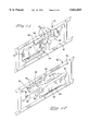
- the two part housing 42 includes a first insulating housing part 44 containing a plurality of signal contacts 46 and a second insulating housing part 48 containing a plurality of power contacts 50.
- Each of the signal contacts has a lead 52 extending out of the housing part 44 and arranged to engage a solder pad 54 on a circuit board 56, as best seen in FIG. 5.
- each of the power contacts 50 has a lead 58 extending out of the housing part 48 and arranged to engage a solder pad 60 on the circuit board 56.
- the two housing parts 44 and 48 are attached to a thin flexible metal strip 62 so that a space 64 remains between the two housing parts, as best seen in FIG. 5.
- the flexible strip 62 is a copper alloy having a width of about 0.125 inch and a thickness of about 0.005 inch.
- the portion 65 of the metal strip 62 that spans the space 64 will permit the two housing parts to mutually move in the direction perpendicular to the plane of the strip but not lateral thereto.
- the flexible strip 62 runs the entire length of the two housing parts 44 and 48 and has a back surface 63 that is flush with the bottom mounting surfaces 66 and 68 of the connector housing 42.
- the connector 40 is mounted to the circuit board 56 in a manner similar to that of the prior art connector 18.
- solder pads 54, 60, and one or more solder pads 72 are coated with solder paste, not shown, and the connector 40 placed in position on the board so that the leads 52 and 58 are embedded in the solder paste and are in engagement with their respective solder pads 54 and 60.
- the circuit board 56 is then supported by its edges on a solder fixture similar to the fixture 16 and placed in a furnace to heat and reflow the solder paste in the usual manner.
- the bottom surface of the strip 62 is soldered to one or more solder pads 72 on the circuit board 56, and the leads 52 and 58 are soldered to their respective solder pads 54 and 60.
- the circuit board 56 exhibits a sag downwardly because it is supported only by its edges 78 and 80 on a solder fixture 82.
- the strip 62 is sufficiently flexible at the portion 65 that it permits the two parts of the connector housing 42 to undergo relative movement in the space 64 to conform somewhat to the curvature of the surface 74 or 76 without one part moving laterally out of position with respect to the other part. This permits the two part housing 42 to align itself on the curved mounting surface as if it were two separate parts, yet maintain position with respect to the solder pads on the circuit board as if it were a single part.
- the housing part 44 aligns itself to the curved surface independently of the housing part 48, and the housing part 48 similarly aligns itself to the curved surface, without adversely affecting the alignment of the leads with respect to their solder pads.
- This avoids the adverse effect of the rigid connector 18 by allowing all of the contact leads 52 and 58 to be relatively closer to their respective solder pads 54 and 60.
- the flexible strip 62 is closer to its solder pads 72 for more of its length than in the prior art case. This has the added advantage of providing more contact area with the solder so that there is increased force via surface tension of the melted solder tending to hold the connector on the circuit board during the solder process.
- the board is inverted on the fixture, as shown in FIG. 9, more solder paste and a second connector 40, not shown, are placed in position of the surface 76 and the entire assembly is again heated in the furnace to solder the second connector to the surface 76.
- the solder holding the first connector 40 is melted allowing the two housing parts of the first connector to conform to the now convex surface 74. Since the back surface 63 of the flexible strip 62 has a relatively large area, compared to the mounting clips 26 in the prior art connector 18, the surface tension of the melted solder in contact with the strip 62, as well as the leads 52 and 58, is sufficiently strong to hold the connector 40 in place on the surface 74, against the force of gravity, as viewed in FIG. 9.
- the connector 40 could be difficult to remove for replacement. Therefore, resistance heating of the strip 62 may be used to melt the solder to facilitate removing the connector 40 from the circuit board 56.
- the tabs 70 are utilized as terminals for attaching leads from a source of electrical current, not shown, for providing the power for the resistance heating.
- a carrier strip 90 has a series of frame openings 92, each of which includes one flexible strip 62, the carrier strip and flexible strip having been formed on a stamping and forming machine in the usual manner.
- Each of the flexible strips 62 are attached to the carrier strip 90 at two points 94 and 96.
- the points 94 and 96 are chosen to be adjacent edges of the finished connector 40 that are accessible by tooling for severing the strip 62 from the carrier strip later.
- the carrier strip 90 which is a so called endless strip supplied on a reel, is feed into a plastic injection mold machine 98.
- the mold machine molds the two housing parts 44 and 48, insitu, onto the flexible strip 62.
- tabs may be stamped and formed integral to the strip that extend into the molded housing parts.
- the back surface 63 in the present example, is flush with the mounting surfaces 66 and 68 of the two housing parts, although it need not be.
- the carrier strip 90 may be feed directly into the contact insertion machine 102 from the mold machine 98, if desired.
- the contact insertion machine 102 inserts the signal contacts 46 into the first housing part 44 and the power contacts 50 into the second housing part 48.
- the connector 40 is arranged on the carrier strip 90 as shown in FIGS. 11 and 12.
- the carrier strip 90, along with the completed connectors 40 may be wound onto a reel, not shown, for later use, or the individual connectors 40 may be separated from the carrier strip by severing at the points 94 and 96, shown in FIG. 12.
- the individual connectors 40 may be packaged in trays or tubes for later use, or the connectors may be inserted into pockets on pocket tape, which is then wound onto a reel for later use.
- the carrier strip 90 emerging from the contact insertion machine 102 may be routed directly to a machine, not shown, for separating the connector from the carrier strip and immediately placing the connector on a circuit board for soldering thereto.
- the two housing parts 44 and 48 are coupled together by a flexible strip 62 with a space 64 between the two housing parts
- other means of coupling will be considered within the teachings of the present invention, such as a projection on one of the parts and a mating receptacle on the other part that holds the two parts together and allows for the necessary relative movement of the parts, or by an elastomeric or other similar resilient member attached to the two housing parts that allows the desired movement.
- the major requirement of the coupling is that flexibility be provided in the direction perpendicular to the mounting surface of the circuit board and substantial rigidity be provided in the direction lateral thereto.
- An important advantage of the present invention is that the two part housing can move to conform somewhat to the curvature or irregularity of the mounting surface of the circuit board, thereby assuring that the contact leads of the connector are close to their respective solder pads during soldering. Another important advantage is that when soldering a connector on the upper side of the circuit board, a connector previously soldered to the other side of the board will be held in place by the increased surface tension due to the flexible strip offering more surface area in contact with the melted solder.
Abstract
An electrical connector (40) having a two part articulated housing (42) is disclosed. The connector, intended for surface mounting on a curved surface (74, 76) of a circuit board (56), includes two housing parts (44, 48) that are intercoupled by means of a flexible member (62) that permits relative movement of the two housing parts in a direction toward and away from the mounting surface but is substantially rigid in the lateral direction. The connector (40) is manufactured by stamping and forming a series of the flexible members (62) on a carrier strip (90), passing the carrier strip through a plastic injection mold machine (98) for molding the two housing parts (44, 48) insitu onto the flexible strip (62), and then passing the carrier strip (90) through a contact insertion machine (102) for inserting the contacts (46,50) into the two housing parts (44, 48).
Description
This application is a Divisional of application Ser. No. 08/429,372 filed Apr. 26, 1995.
The present invention is related to electrical connectors of the type that are surface mounted to circuitry on relatively thin flexible circuit boards, and more particularly to such connectors that are capable of accommodating the curved mounting surfaces which may be associated with these boards.
Electronic equipment, such as computers and cellular telephones, typically contain various circuit boards that in turn contain electronic components that are interconnected via metalized circuitry on the circuit boards. Electrical connectors are frequently used to interconnect a circuit board to other circuit boards or to other components of the equipment. With the continuing advance of electronic technology, the individual components of the electronic equipment are made smaller resulting in miniaturized but highly dense packages. Circuit board technology has similarly migrated toward smaller and thinner structures. When a connector is surface mounted to a circuit board, the contact leads of the connector must be brought into mated engagement with respective solder pads on the circuit board and held there during soldering. Typically, solder paste is applied to the solder pads on one side of the circuit board and a connector and electrical components placed in position with their leads embedded in the solder paste and in contact with the pads. The circuit board is placed in a fixture which is then placed in a furnace and subjected to heat to reflow the solder and complete the electrical connection between the leads of the connector and the circuitry. If the circuit board is double sided it is then turned over and the process repeated so that a connector and components are soldered to circuitry on both sides of the circuit board. By way of example, as shown schematically in FIG. 1, a circuit board 10 is supported at its edges 12 and 14 by a fixture 16. A prior art electrical connector 18, shown in plan view in FIG. 2, is in position on the top surface 28 of the circuit board, prior to soldering, and another similar connector 19 that had been previously soldered in place is on the lower surface 30. The connector 18, in the present example, includes an insulating housing 20, four leads 22 from power contacts and several leads 24 from signal contacts, contained within the housing. Three mounting clips 26 are arranged in openings in the housing so that they are flush with the bottom mounting surface of the housing. FIGS. 3 and 4 are enlarged views of a portion of the circuit board 10 shown in FIG. 1. As shown in FIG. 3, when the circuit board is quite thin it will sag downwardly a substantial amount while it is being supported by its edges. This results in the top surface 28, against which the connector 18 is resting, being concave. This concave condition of the circuit board may also be aggravated by distortions caused during the manufacture of the circuit board. When the connector 18 is moderately long the leads 22' and 24' and the clip 26 near the center of the connector may be sufficiently spaced from the surface 28 so that they will not be soldered to their respective solder pads during the soldering operation. Additionally, the connector 19 which was previously soldered to the surface 30 when the circuit board 10 was reversed, will now be on the lower side of the circuit board, as shown in FIG. 4. Since the circuit board 10 sags downwardly the lower surface 30 is convex. When the circuit board is again heated to reflow the solder paste on the upper surface 28 the solder on the lower surface 30 will melt causing the leads 22' and 24' and the clips 26 near the ends of the connector 19 to lift off of the surface 30. If the space between the leads and their solder pads is great enough the solder will separate, due to surface tension, and there will be no electrical connection upon completion of the soldering operation. Additionally, the reduced contact with the melted solder yields less holding force due to surface tension, therefore, the connector 19 may fall off of the circuit board while soldering the connector 18 in place. While the particular prior art connector 18, in the present example, has the above described problems, so too do other similar connectors that are rather long and intended for mounting to relatively thin flexible circuit boards that are supported at their edges during soldering.
What is needed is an electrical connector that will conform sufficiently to the curved surface of the circuit board so that the leads remain sufficiently close to their respective solder pads to assure a good soldered connection and, to provide sufficient area in contact with the melted solder to retain the connector in place on the under side of the circuit board when a connector is being soldered on the upper side.
An electrical connector is provided having a two part articulated housing for surface mounting to a curved mounting surface of a circuit board. A first housing part of insulating material is provided containing a plurality of first electrical contacts therein for mating with contacts in a mating connector. The first electrical contacts have leads extending out of the first housing part that are arranged to engage first solder pads on the mounting surface. A second housing part of insulating material is provided containing a plurality of second electrical contacts therein for mating with contacts in the mating connector. The second electrical contacts have leads extending out of the second housing part that are arranged to engage second solder pads on the mounting surface. A flexible coupling interconnects the first and second housing parts. The coupling is arranged so that when the connector is placed upon the curved mounting surface with solder paste therebetween, the first and second housing parts mutually deflect so that the leads of the first and second electrical contacts engage and are embedded in the solder paste.
FIG. 1 is a schematic view of a circuit board and two prior art connectors arranged on a solder fixture preparatory to soldering;
FIG. 2 is a front view of the prior art connector shown in FIG. 1;
FIGS. 3 and 4 are enlarged views of portions of the view of FIG. 1;
FIGS. 5, 6, and 7 are front, side, and rear views, respectively, of an electrical connector incorporating the teachings of the present invention, FIGS. 5 and 6 showing the connector on a circuit board;
FIGS. 8 and 9 are side views of the connector shown in FIG. 5, on a curved mounting surface of a circuit board;
FIG. 10 is a schematic view showing the process of making the connector shown in FIG. 5; and
FIGS. 11 and 12 are isometric views of the front and rear, respectively, of the connector shown in FIG. 5.
There is shown in FIGS. 5, 6, and 7, an electrical connector 40 having a two part articulated housing 42. The two part housing 42 includes a first insulating housing part 44 containing a plurality of signal contacts 46 and a second insulating housing part 48 containing a plurality of power contacts 50. Each of the signal contacts has a lead 52 extending out of the housing part 44 and arranged to engage a solder pad 54 on a circuit board 56, as best seen in FIG. 5. Similarly, each of the power contacts 50 has a lead 58 extending out of the housing part 48 and arranged to engage a solder pad 60 on the circuit board 56. The two housing parts 44 and 48 are attached to a thin flexible metal strip 62 so that a space 64 remains between the two housing parts, as best seen in FIG. 5. The flexible strip 62 is a copper alloy having a width of about 0.125 inch and a thickness of about 0.005 inch. The portion 65 of the metal strip 62 that spans the space 64 will permit the two housing parts to mutually move in the direction perpendicular to the plane of the strip but not lateral thereto. The flexible strip 62 runs the entire length of the two housing parts 44 and 48 and has a back surface 63 that is flush with the bottom mounting surfaces 66 and 68 of the connector housing 42. There is a tab 70 at each end of the strip 62 bent at right angles thereto away from the mounting surfaces 66 and 68, for a purpose that will be explained. In practice, generally, the connector 40 is mounted to the circuit board 56 in a manner similar to that of the prior art connector 18. The solder pads 54, 60, and one or more solder pads 72 are coated with solder paste, not shown, and the connector 40 placed in position on the board so that the leads 52 and 58 are embedded in the solder paste and are in engagement with their respective solder pads 54 and 60. The circuit board 56 is then supported by its edges on a solder fixture similar to the fixture 16 and placed in a furnace to heat and reflow the solder paste in the usual manner. The bottom surface of the strip 62 is soldered to one or more solder pads 72 on the circuit board 56, and the leads 52 and 58 are soldered to their respective solder pads 54 and 60.
As shown in FIGS. 8 and 9, the circuit board 56 exhibits a sag downwardly because it is supported only by its edges 78 and 80 on a solder fixture 82. The strip 62 is sufficiently flexible at the portion 65 that it permits the two parts of the connector housing 42 to undergo relative movement in the space 64 to conform somewhat to the curvature of the surface 74 or 76 without one part moving laterally out of position with respect to the other part. This permits the two part housing 42 to align itself on the curved mounting surface as if it were two separate parts, yet maintain position with respect to the solder pads on the circuit board as if it were a single part. That is, the housing part 44 aligns itself to the curved surface independently of the housing part 48, and the housing part 48 similarly aligns itself to the curved surface, without adversely affecting the alignment of the leads with respect to their solder pads. This avoids the adverse effect of the rigid connector 18 by allowing all of the contact leads 52 and 58 to be relatively closer to their respective solder pads 54 and 60. Additionally, the flexible strip 62 is closer to its solder pads 72 for more of its length than in the prior art case. This has the added advantage of providing more contact area with the solder so that there is increased force via surface tension of the melted solder tending to hold the connector on the circuit board during the solder process. After soldering the first connector 40 to the surface 74 of the circuit board 56, as shown in FIG. 8, the board is inverted on the fixture, as shown in FIG. 9, more solder paste and a second connector 40, not shown, are placed in position of the surface 76 and the entire assembly is again heated in the furnace to solder the second connector to the surface 76. During this process the solder holding the first connector 40 is melted allowing the two housing parts of the first connector to conform to the now convex surface 74. Since the back surface 63 of the flexible strip 62 has a relatively large area, compared to the mounting clips 26 in the prior art connector 18, the surface tension of the melted solder in contact with the strip 62, as well as the leads 52 and 58, is sufficiently strong to hold the connector 40 in place on the surface 74, against the force of gravity, as viewed in FIG. 9. Since a substantial portion of the bottom surface of the flexible strip 62 is soldered to the pads 72, the connector 40 could be difficult to remove for replacement. Therefore, resistance heating of the strip 62 may be used to melt the solder to facilitate removing the connector 40 from the circuit board 56. The tabs 70 are utilized as terminals for attaching leads from a source of electrical current, not shown, for providing the power for the resistance heating.
The process of manufacturing the connector 40 will now be discussed, with reference to FIGS. 10, 11, and 12. As shown in FIG. 10, a carrier strip 90 has a series of frame openings 92, each of which includes one flexible strip 62, the carrier strip and flexible strip having been formed on a stamping and forming machine in the usual manner. Each of the flexible strips 62 are attached to the carrier strip 90 at two points 94 and 96. The points 94 and 96 are chosen to be adjacent edges of the finished connector 40 that are accessible by tooling for severing the strip 62 from the carrier strip later. As shown schematically in FIG. 10, the carrier strip 90, which is a so called endless strip supplied on a reel, is feed into a plastic injection mold machine 98. The mold machine molds the two housing parts 44 and 48, insitu, onto the flexible strip 62. To enhance mechanical attachment of the two housing parts to the strip 62, tabs may be stamped and formed integral to the strip that extend into the molded housing parts. Note that the back surface 63, in the present example, is flush with the mounting surfaces 66 and 68 of the two housing parts, although it need not be. As the carrier strip 90 emerges from the mold machine 98, as shown in FIG. 10, the strip with the two housing parts 44 and 48 attached to each flexible strip 62, is wound onto a reel 100, for later processing. The carrier strip 90, along with the attached connector housings 42, is later dereeled from the reel 100 and fed into a contact insertion machine 102. Optionally, the carrier strip 90 may be feed directly into the contact insertion machine 102 from the mold machine 98, if desired. The contact insertion machine 102 inserts the signal contacts 46 into the first housing part 44 and the power contacts 50 into the second housing part 48. As the carrier strip 90 emerges from the contact insertion machine 102, the connector 40 is arranged on the carrier strip 90 as shown in FIGS. 11 and 12. The carrier strip 90, along with the completed connectors 40 may be wound onto a reel, not shown, for later use, or the individual connectors 40 may be separated from the carrier strip by severing at the points 94 and 96, shown in FIG. 12. In the case of separating the connector from the carrier strip, the individual connectors 40 may be packaged in trays or tubes for later use, or the connectors may be inserted into pockets on pocket tape, which is then wound onto a reel for later use. Alternatively, the carrier strip 90 emerging from the contact insertion machine 102 may be routed directly to a machine, not shown, for separating the connector from the carrier strip and immediately placing the connector on a circuit board for soldering thereto.
While, in the present example, the two housing parts 44 and 48 are coupled together by a flexible strip 62 with a space 64 between the two housing parts, other means of coupling will be considered within the teachings of the present invention, such as a projection on one of the parts and a mating receptacle on the other part that holds the two parts together and allows for the necessary relative movement of the parts, or by an elastomeric or other similar resilient member attached to the two housing parts that allows the desired movement. The major requirement of the coupling is that flexibility be provided in the direction perpendicular to the mounting surface of the circuit board and substantial rigidity be provided in the direction lateral thereto.
An important advantage of the present invention is that the two part housing can move to conform somewhat to the curvature or irregularity of the mounting surface of the circuit board, thereby assuring that the contact leads of the connector are close to their respective solder pads during soldering. Another important advantage is that when soldering a connector on the upper side of the circuit board, a connector previously soldered to the other side of the board will be held in place by the increased surface tension due to the flexible strip offering more surface area in contact with the melted solder.
Claims (3)
1. In a method of making an electrical connector having a two part articulated housing and electrical contacts therein, the steps:
(1) providing a carrier strip having a flexible metal member attached thereto;
(2) molding insitu a first housing part and a second housing part onto said flexible member, said first and second housing parts being mutually spaced apart;
(3) transporting said carrier strip to a contact insertion machine; and
(4) inserting said electrical contacts into said first and second housings.
2. The method according to claim 1 including after step (4) the following step:
(5) removing said flexible member including attached first and second housing parts from said carrier strip.
3. The method according to claim 10 wherein said molding of step (2) includes molding said first and second housing parts with first mounting surfaces that are flush with said flexible metal member.
Priority Applications (1)
| Application Number | Priority Date | Filing Date | Title |
|---|---|---|---|
| US08/620,375 US5822855A (en) | 1995-04-26 | 1996-03-22 | Method of making electrical connector having a two part articulated housing |
Applications Claiming Priority (2)
| Application Number | Priority Date | Filing Date | Title |
|---|---|---|---|
| US08/429,372 US5667391A (en) | 1995-04-26 | 1995-04-26 | Electrical connector having a two part articulated housing |
| US08/620,375 US5822855A (en) | 1995-04-26 | 1996-03-22 | Method of making electrical connector having a two part articulated housing |
Related Parent Applications (1)
| Application Number | Title | Priority Date | Filing Date |
|---|---|---|---|
| US08/429,372 Division US5667391A (en) | 1995-04-26 | 1995-04-26 | Electrical connector having a two part articulated housing |
Publications (1)
| Publication Number | Publication Date |
|---|---|
| US5822855A true US5822855A (en) | 1998-10-20 |
Family
ID=23702956
Family Applications (2)
| Application Number | Title | Priority Date | Filing Date |
|---|---|---|---|
| US08/429,372 Expired - Lifetime US5667391A (en) | 1995-04-26 | 1995-04-26 | Electrical connector having a two part articulated housing |
| US08/620,375 Expired - Fee Related US5822855A (en) | 1995-04-26 | 1996-03-22 | Method of making electrical connector having a two part articulated housing |
Family Applications Before (1)
| Application Number | Title | Priority Date | Filing Date |
|---|---|---|---|
| US08/429,372 Expired - Lifetime US5667391A (en) | 1995-04-26 | 1995-04-26 | Electrical connector having a two part articulated housing |
Country Status (2)
| Country | Link |
|---|---|
| US (2) | US5667391A (en) |
| WO (1) | WO1996034433A1 (en) |
Cited By (24)
| Publication number | Priority date | Publication date | Assignee | Title |
|---|---|---|---|---|
| US6162091A (en) * | 1998-08-03 | 2000-12-19 | Fujitsu Takamisawa Component Limited | Connector |
| US6203335B1 (en) * | 1999-12-22 | 2001-03-20 | Hon Hai Precision Ind. Co., Ltd. | Mobile phone connector and the art of assembly of contacts and a housing |
| US6360438B1 (en) * | 1999-11-23 | 2002-03-26 | Delphi Technologies, Inc. | Method of making an upper housing for a bussed electrical center |
| US20060057896A1 (en) * | 2004-09-10 | 2006-03-16 | Arvind Karir | Multiple port electrical connector |
| US20100062630A1 (en) * | 2008-03-13 | 2010-03-11 | Wen Chang Chang | Electrical connector |
| US20110215368A1 (en) * | 2010-03-05 | 2011-09-08 | Johnny Chen | Light-emitting diode with wire-piercing lead frame |
| US8469750B2 (en) | 2011-09-22 | 2013-06-25 | Willis Electric Co., Ltd. | LED lamp assembly and light strings including a lamp assembly |
| GB2505049A (en) * | 2012-06-20 | 2014-02-19 | Lear Corp Gmbh | Positioning element and mold arrangement |
| US8920002B2 (en) | 2011-06-21 | 2014-12-30 | Willis Electric Co., Ltd. | Wire-clasping light-emitting diode lights |
| US9044056B2 (en) | 2012-05-08 | 2015-06-02 | Willis Electric Co., Ltd. | Modular tree with electrical connector |
| US9055777B2 (en) | 2010-09-23 | 2015-06-16 | Willis Electric Co., Ltd. | Modular artificial lighted tree with decorative light string |
| US9157587B2 (en) | 2011-11-14 | 2015-10-13 | Willis Electric Co., Ltd. | Conformal power adapter for lighted artificial tree |
| US9220361B1 (en) | 2013-12-03 | 2015-12-29 | Willis Electric Co., Ltd. | Dual-voltage lighted artificial tree |
| US9222656B2 (en) | 2011-11-14 | 2015-12-29 | Willis Electric Co., Ltd. | Conformal power adapter for lighted artificial tree |
| US9441800B1 (en) | 2011-12-09 | 2016-09-13 | Willis Electric Co., Ltd. | Modular lighted artificial tree |
| US9439528B2 (en) | 2013-03-13 | 2016-09-13 | Willis Electric Co., Ltd. | Modular tree with locking trunk and locking electrical connectors |
| US9572446B2 (en) | 2012-05-08 | 2017-02-21 | Willis Electric Co., Ltd. | Modular tree with locking trunk and locking electrical connectors |
| US9648919B2 (en) | 2012-05-08 | 2017-05-16 | Willis Electric Co., Ltd. | Modular tree with rotation-lock electrical connectors |
| US9671074B2 (en) | 2013-03-13 | 2017-06-06 | Willis Electric Co., Ltd. | Modular tree with trunk connectors |
| US9883566B1 (en) | 2014-05-01 | 2018-01-30 | Willis Electric Co., Ltd. | Control of modular lighted artificial trees |
| US9883706B2 (en) | 2011-05-20 | 2018-02-06 | Willis Electric Co., Ltd. | Multi-positional, locking artificial tree trunk |
| US9894949B1 (en) | 2013-11-27 | 2018-02-20 | Willis Electric Co., Ltd. | Lighted artificial tree with improved electrical connections |
| US10206530B2 (en) | 2012-05-08 | 2019-02-19 | Willis Electric Co., Ltd. | Modular tree with locking trunk |
| US10683974B1 (en) | 2017-12-11 | 2020-06-16 | Willis Electric Co., Ltd. | Decorative lighting control |
Families Citing this family (1)
| Publication number | Priority date | Publication date | Assignee | Title |
|---|---|---|---|---|
| US9129942B2 (en) * | 2012-06-05 | 2015-09-08 | International Business Machines Corporation | Method for shaping a laminate substrate |
Citations (10)
| Publication number | Priority date | Publication date | Assignee | Title |
|---|---|---|---|---|
| US4337574A (en) * | 1978-12-14 | 1982-07-06 | Amp Incorporated | Method of manufacturing electrical connector receptacles |
| US4445736A (en) * | 1982-03-31 | 1984-05-01 | Amp Incorporated | Method and apparatus for producing a premolded packaging |
| US4602429A (en) * | 1984-01-06 | 1986-07-29 | Burndy Corporation | Method and apparatus for assembling electrical connectors |
| US4807283A (en) * | 1985-06-13 | 1989-02-21 | Oy Nokia Ab | Method for adjusting the balancing impedance of a hybrid junction |
| US4975067A (en) * | 1989-09-27 | 1990-12-04 | Elsag International B.V. | Surface contact power connector |
| JPH04159792A (en) * | 1990-10-23 | 1992-06-02 | Tamura Seisakusho Co Ltd | Metallic core substrate |
| US5282751A (en) * | 1991-07-31 | 1994-02-01 | Nai Hock Lwee | Connector apparatus |
| US5380222A (en) * | 1992-04-16 | 1995-01-10 | Canon Kabushiki Kaisha | Connector for circuit boards, and device using same |
| US5406458A (en) * | 1993-03-11 | 1995-04-11 | Ncr Corporation | Printed circuit board having tapered contact pads for surface mounted electrical components |
| WO1995010865A1 (en) * | 1993-10-14 | 1995-04-20 | Berg Electronics Manufacturing B.V. | Electrical connector for mounting on the surface of a printed circuit board |
Family Cites Families (2)
| Publication number | Priority date | Publication date | Assignee | Title |
|---|---|---|---|---|
| DE1252262B (en) * | 1967-10-19 | |||
| US5461774A (en) * | 1994-03-25 | 1995-10-31 | Motorola, Inc. | Apparatus and method of elastically bowing a base plate |
-
1995
- 1995-04-26 US US08/429,372 patent/US5667391A/en not_active Expired - Lifetime
-
1996
- 1996-02-21 WO PCT/US1996/002484 patent/WO1996034433A1/en active Application Filing
- 1996-03-22 US US08/620,375 patent/US5822855A/en not_active Expired - Fee Related
Patent Citations (10)
| Publication number | Priority date | Publication date | Assignee | Title |
|---|---|---|---|---|
| US4337574A (en) * | 1978-12-14 | 1982-07-06 | Amp Incorporated | Method of manufacturing electrical connector receptacles |
| US4445736A (en) * | 1982-03-31 | 1984-05-01 | Amp Incorporated | Method and apparatus for producing a premolded packaging |
| US4602429A (en) * | 1984-01-06 | 1986-07-29 | Burndy Corporation | Method and apparatus for assembling electrical connectors |
| US4807283A (en) * | 1985-06-13 | 1989-02-21 | Oy Nokia Ab | Method for adjusting the balancing impedance of a hybrid junction |
| US4975067A (en) * | 1989-09-27 | 1990-12-04 | Elsag International B.V. | Surface contact power connector |
| JPH04159792A (en) * | 1990-10-23 | 1992-06-02 | Tamura Seisakusho Co Ltd | Metallic core substrate |
| US5282751A (en) * | 1991-07-31 | 1994-02-01 | Nai Hock Lwee | Connector apparatus |
| US5380222A (en) * | 1992-04-16 | 1995-01-10 | Canon Kabushiki Kaisha | Connector for circuit boards, and device using same |
| US5406458A (en) * | 1993-03-11 | 1995-04-11 | Ncr Corporation | Printed circuit board having tapered contact pads for surface mounted electrical components |
| WO1995010865A1 (en) * | 1993-10-14 | 1995-04-20 | Berg Electronics Manufacturing B.V. | Electrical connector for mounting on the surface of a printed circuit board |
Non-Patent Citations (2)
| Title |
|---|
| New Electronics: No. 16, Aug. 17, 1984, London, GB; pp. 29 32; XP002005801; G.R. Latham: Surface Mount with Flexible Circuits:. * |
| New Electronics: No. 16, Aug. 17, 1984, London, GB; pp. 29-32; XP002005801; G.R. Latham: Surface Mount with Flexible Circuits:. |
Cited By (44)
| Publication number | Priority date | Publication date | Assignee | Title |
|---|---|---|---|---|
| US6162091A (en) * | 1998-08-03 | 2000-12-19 | Fujitsu Takamisawa Component Limited | Connector |
| US6360438B1 (en) * | 1999-11-23 | 2002-03-26 | Delphi Technologies, Inc. | Method of making an upper housing for a bussed electrical center |
| US6203335B1 (en) * | 1999-12-22 | 2001-03-20 | Hon Hai Precision Ind. Co., Ltd. | Mobile phone connector and the art of assembly of contacts and a housing |
| US20060057896A1 (en) * | 2004-09-10 | 2006-03-16 | Arvind Karir | Multiple port electrical connector |
| US7140923B2 (en) | 2004-09-10 | 2006-11-28 | Amphenol Corporation | Multiple port electrical connector |
| US20100062630A1 (en) * | 2008-03-13 | 2010-03-11 | Wen Chang Chang | Electrical connector |
| US7874875B2 (en) * | 2008-03-13 | 2011-01-25 | Lotes Co., Ltd. | Electrical connector |
| US8853721B2 (en) | 2010-03-05 | 2014-10-07 | Willis Electric Co., Ltd. | Light-emitting diode with wire-piercing lead frame |
| US20110215368A1 (en) * | 2010-03-05 | 2011-09-08 | Johnny Chen | Light-emitting diode with wire-piercing lead frame |
| US8608342B2 (en) | 2010-03-05 | 2013-12-17 | Willis Electric Co., Ltd. | Wire-piercing light-emitting diode light strings |
| US10070675B2 (en) | 2010-09-23 | 2018-09-11 | Willis Electric Co., Ltd. | Modular lighted tree with internal electrical connection system |
| US9484687B1 (en) | 2010-09-23 | 2016-11-01 | Willis Electric Co., Ltd. | Modular lighted tree |
| US9887501B2 (en) | 2010-09-23 | 2018-02-06 | Willis Electric Co., Ltd. | Modular artificial lighted tree with decorative light string |
| US9055777B2 (en) | 2010-09-23 | 2015-06-16 | Willis Electric Co., Ltd. | Modular artificial lighted tree with decorative light string |
| US9861147B1 (en) | 2010-09-23 | 2018-01-09 | Willis Electric Co., Ltd. | Modular lighted tree |
| US9883706B2 (en) | 2011-05-20 | 2018-02-06 | Willis Electric Co., Ltd. | Multi-positional, locking artificial tree trunk |
| US8920002B2 (en) | 2011-06-21 | 2014-12-30 | Willis Electric Co., Ltd. | Wire-clasping light-emitting diode lights |
| US8747167B2 (en) | 2011-09-22 | 2014-06-10 | Willis Electric Co., Ltd. | LED lamp assembly and light strings including a lamp assembly |
| US8469750B2 (en) | 2011-09-22 | 2013-06-25 | Willis Electric Co., Ltd. | LED lamp assembly and light strings including a lamp assembly |
| US9157587B2 (en) | 2011-11-14 | 2015-10-13 | Willis Electric Co., Ltd. | Conformal power adapter for lighted artificial tree |
| US9222656B2 (en) | 2011-11-14 | 2015-12-29 | Willis Electric Co., Ltd. | Conformal power adapter for lighted artificial tree |
| US9677749B2 (en) | 2011-11-14 | 2017-06-13 | Willis Electric Co., Ltd. | Conformal power adapter for lighted artificial tree |
| US9664362B2 (en) | 2011-11-14 | 2017-05-30 | Willis Electric Co., Ltd. | Lighted artificial tree with multi-terminal electrical connectors for power distribution and control |
| US9441823B1 (en) | 2011-12-09 | 2016-09-13 | Willis Electric Co., Ltd. | Modular lighted artificial tree |
| US9441800B1 (en) | 2011-12-09 | 2016-09-13 | Willis Electric Co., Ltd. | Modular lighted artificial tree |
| US9044056B2 (en) | 2012-05-08 | 2015-06-02 | Willis Electric Co., Ltd. | Modular tree with electrical connector |
| US9572446B2 (en) | 2012-05-08 | 2017-02-21 | Willis Electric Co., Ltd. | Modular tree with locking trunk and locking electrical connectors |
| US9648919B2 (en) | 2012-05-08 | 2017-05-16 | Willis Electric Co., Ltd. | Modular tree with rotation-lock electrical connectors |
| US10206530B2 (en) | 2012-05-08 | 2019-02-19 | Willis Electric Co., Ltd. | Modular tree with locking trunk |
| US9526286B2 (en) | 2012-05-08 | 2016-12-27 | Willis Electric Co., Ltd. | Modular tree with electrical connector |
| US10010208B2 (en) | 2012-05-08 | 2018-07-03 | Willis Electric Co., Ltd. | Modular tree with electrical connector |
| GB2505049A (en) * | 2012-06-20 | 2014-02-19 | Lear Corp Gmbh | Positioning element and mold arrangement |
| US9743544B2 (en) | 2012-06-20 | 2017-08-22 | Lear Corporation | Positioning element |
| GB2505049B (en) * | 2012-06-20 | 2015-04-29 | Lear Corp Gmbh | A housing part having a positioning element and method for producing same |
| US10098491B2 (en) | 2013-03-13 | 2018-10-16 | Willis Electric Co., Ltd. | Modular tree with locking trunk and locking electrical connectors |
| US9671074B2 (en) | 2013-03-13 | 2017-06-06 | Willis Electric Co., Ltd. | Modular tree with trunk connectors |
| US9439528B2 (en) | 2013-03-13 | 2016-09-13 | Willis Electric Co., Ltd. | Modular tree with locking trunk and locking electrical connectors |
| US9894949B1 (en) | 2013-11-27 | 2018-02-20 | Willis Electric Co., Ltd. | Lighted artificial tree with improved electrical connections |
| US9220361B1 (en) | 2013-12-03 | 2015-12-29 | Willis Electric Co., Ltd. | Dual-voltage lighted artificial tree |
| US9677748B1 (en) | 2013-12-03 | 2017-06-13 | Willis Electric Co., Ltd. | Dual-voltage lighted artificial tree |
| US9883566B1 (en) | 2014-05-01 | 2018-01-30 | Willis Electric Co., Ltd. | Control of modular lighted artificial trees |
| US10683974B1 (en) | 2017-12-11 | 2020-06-16 | Willis Electric Co., Ltd. | Decorative lighting control |
| US10989374B1 (en) | 2017-12-11 | 2021-04-27 | Willis Electric Co., Ltd. | Decorative lighting control |
| US11353176B1 (en) | 2017-12-11 | 2022-06-07 | Willis Electric Co., Ltd. | Decorative lighting control |
Also Published As
| Publication number | Publication date |
|---|---|
| WO1996034433A1 (en) | 1996-10-31 |
| US5667391A (en) | 1997-09-16 |
Similar Documents
| Publication | Publication Date | Title |
|---|---|---|
| US5822855A (en) | Method of making electrical connector having a two part articulated housing | |
| US6398559B2 (en) | Connecting terminal and a connecting terminal assembly | |
| KR100586124B1 (en) | Circuit board of protective circuit for storage battery, protective circuit for storage battery, and storage battery pack | |
| US5899760A (en) | Connector assembly | |
| US5334059A (en) | Solder-bearing lead | |
| JPS62502926A (en) | Solder holding lead wire | |
| JP2000506663A (en) | Battery connector | |
| JPS61116782A (en) | Back board connector | |
| EP0303873B1 (en) | Conductive lead arrangement | |
| US6287151B1 (en) | Electrical connector for manipulation by a vacuum-suction nozzle | |
| US4897047A (en) | Electrically and mechanically programmable electrical apparatus | |
| KR100735351B1 (en) | Wiring board having connector and method of manufacturing the same | |
| US4158877A (en) | Connecting and supporting clamp for two adjacently situated printed circuit cards | |
| EP1010217B1 (en) | Edge mount connector having locating recesses for solder tail registration | |
| US4401352A (en) | Connector system for connecting a ceramic substrate to a printed circuit board | |
| US6846190B2 (en) | IC socket and gripping sheet used in the same | |
| US5226825A (en) | Surface mount chip carrier socket | |
| JPH11345675A (en) | Manufacture of electric connector | |
| JPH0719102Y2 (en) | Flat cable connector | |
| US5279508A (en) | Shifting connection device | |
| US20040077193A1 (en) | Board mounted electrical connector | |
| AU583396B2 (en) | Solder bearing leads | |
| JP2000251986A (en) | Electrical connector | |
| US5667874A (en) | Embossed tape with oblique housing portions for packaging parts | |
| US20030153201A1 (en) | Circuit board electrical lead frame |
Legal Events
| Date | Code | Title | Description |
|---|---|---|---|
| FPAY | Fee payment |
Year of fee payment: 4 |
|
| FPAY | Fee payment |
Year of fee payment: 8 |
|
| REMI | Maintenance fee reminder mailed | ||
| LAPS | Lapse for failure to pay maintenance fees | ||
| STCH | Information on status: patent discontinuation |
Free format text: PATENT EXPIRED DUE TO NONPAYMENT OF MAINTENANCE FEES UNDER 37 CFR 1.362 |
|
| FP | Lapsed due to failure to pay maintenance fee |
Effective date: 20101020 |