US5828607A - Memory programming circuit and method - Google Patents
Memory programming circuit and method Download PDFInfo
- Publication number
- US5828607A US5828607A US08/861,078 US86107897A US5828607A US 5828607 A US5828607 A US 5828607A US 86107897 A US86107897 A US 86107897A US 5828607 A US5828607 A US 5828607A
- Authority
- US
- United States
- Prior art keywords
- voltage
- circuit
- pumped
- transistor
- coupled
- Prior art date
- Legal status (The legal status is an assumption and is not a legal conclusion. Google has not performed a legal analysis and makes no representation as to the accuracy of the status listed.)
- Expired - Lifetime
Links
- 238000000034 method Methods 0.000 title claims abstract description 14
- 230000004044 response Effects 0.000 claims abstract description 20
- 230000004913 activation Effects 0.000 claims 1
- 238000012544 monitoring process Methods 0.000 claims 1
- 238000005086 pumping Methods 0.000 claims 1
- 230000015556 catabolic process Effects 0.000 abstract description 13
- 230000004048 modification Effects 0.000 abstract description 2
- 238000012986 modification Methods 0.000 abstract description 2
- 238000010586 diagram Methods 0.000 description 27
- 230000036039 immunity Effects 0.000 description 8
- PWPJGUXAGUPAHP-UHFFFAOYSA-N lufenuron Chemical compound C1=C(Cl)C(OC(F)(F)C(C(F)(F)F)F)=CC(Cl)=C1NC(=O)NC(=O)C1=C(F)C=CC=C1F PWPJGUXAGUPAHP-UHFFFAOYSA-N 0.000 description 8
- 230000007704 transition Effects 0.000 description 5
- 230000008569 process Effects 0.000 description 4
- 239000004020 conductor Substances 0.000 description 3
- 230000006870 function Effects 0.000 description 3
- 238000004519 manufacturing process Methods 0.000 description 3
- 230000001052 transient effect Effects 0.000 description 3
- 208000033999 Device damage Diseases 0.000 description 2
- 230000001413 cellular effect Effects 0.000 description 2
- 230000003213 activating effect Effects 0.000 description 1
- 239000000284 extract Substances 0.000 description 1
- 239000004973 liquid crystal related substance Substances 0.000 description 1
- 239000011159 matrix material Substances 0.000 description 1
- 230000002028 premature Effects 0.000 description 1
- 239000004065 semiconductor Substances 0.000 description 1
- 230000035945 sensitivity Effects 0.000 description 1
- 238000012163 sequencing technique Methods 0.000 description 1
- 230000005236 sound signal Effects 0.000 description 1
- 230000005641 tunneling Effects 0.000 description 1
Images


Classifications
-
- G—PHYSICS
- G11—INFORMATION STORAGE
- G11C—STATIC STORES
- G11C16/00—Erasable programmable read-only memories
- G11C16/02—Erasable programmable read-only memories electrically programmable
- G11C16/06—Auxiliary circuits, e.g. for writing into memory
- G11C16/10—Programming or data input circuits
- G11C16/12—Programming voltage switching circuits
-
- G—PHYSICS
- G11—INFORMATION STORAGE
- G11C—STATIC STORES
- G11C16/00—Erasable programmable read-only memories
- G11C16/02—Erasable programmable read-only memories electrically programmable
- G11C16/06—Auxiliary circuits, e.g. for writing into memory
- G11C16/30—Power supply circuits
Definitions
- the present invention relates in general to memory circuits, and more particularly to high voltage power supplies for programming nonvolatile memory circuits.
- Wireless communications systems are presently using digital techniques to increase functionality and noise immunity while reducing cost.
- cellular telephones and pagers receive radio frequency carrier signals modulated With digital data.
- a digital signal processor receives the digital data from a demodulator and executes a preprogrammed software algorithm to convert the data to audio and display signals.
- the preprogrammed software algorithm, as well as control signals, downloaded data, and the like, typically are stored in a nonvolatile memory.
- the nonvolatile memory circuit When such wireless communications devices are for portable use, the nonvolatile memory circuit must operate from a low level battery, e.g., 1.8 volts, and have minimum current drain in order to extend the operating time between battery recharges. In addition, the die size of the nonvolatile memory circuits should be kept as small as possible in order to control manufacturing cost.
- a low level battery e.g., 1.8 volts
- Nonvolatile memory circuits often use electrically erasable, floating gate transistors as storage elements. Stored data is modified by applying high voltage signals to induce a tunneling current through a gate dielectric which results in charging the floating gate to a predetermined potential to alter the transistor's conduction.
- Prior art memory circuits are fabricated on a high voltage transistor process to prevent the high voltages from breaking down the programming transistors.
- a problem with such processes is that the high voltage transistors consume a larger die area than transistors fabricated on a low voltage process, which increases the cost of the memory circuit.
- the larger devices are slower and have higher conduction thresholds, which reduces speed and results in poor performance when powered from a 1.8 volt battery.
- FIG. 1 is a block diagram of a wireless communications device
- FIG. 2 is a block diagram of memory circuit
- FIG. 3 is a schematic diagram of a nonvolatile memory cell
- FIG. 4 is a schematic diagram of an output buffer stage of a row driver
- FIG. 5 is a block diagram of a memory power circuit
- FIG. 6 is a schematic diagram of a voltage monitor circuit
- FIG. 7 is a schematic diagram of another voltage monitor circuit.
- FIG. 8 is a schematic diagram of a voltage generator
- FIG. 9 is a schematic diagram of another voltage generator
- FIG. 10 is a schematic diagram of a switch
- FIG. 11 is a schematic diagram of another switch
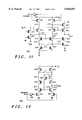
- FIG. 12 is a schematic diagram of a level shifting circuit
- FIG. 13 is a schematic diagram of another level shifting circuit.
- FIG. 14 is a schematic diagram of yet another level shifting circuit.
- FIG. 1 shows a block diagram of a wireless communications device 100 such as a cellular telephone, two-way radio or pager.
- a receiver circuit in communications device 100 includes an antenna 102, a radio frequency (RF) circuit 104 and a demodulator 106.
- Antenna 102 receives a transmitted RF carrier signal modulated with digital information.
- RF circuit 104 amplifies the RF carrier signal and converts the frequency down to an intermediate frequency (IF) signal which is applied to an input of demodulator 106.
- Demodulator 106 extracts the digital information from the IF signal to produce baseband digital data which is applied to an input of a digital signal processor (DSP) circuit 108.
- DSP digital signal processor
- the software is addressed by sending an ADDR logic signal to memory circuit 110. Transfers of DATA between DSP 108 and memory circuit 110 are made using a data bus.
- a PROG/ERASE signal is transferred on two conductors such that one conductor carries a PROG logic signal to control when selected memory cells are programmed and the other conductor carries an ERASE logic signal to control when selected memory cells are erased.
- DSP 108 produces video and control signals for driving a display device 114, such as a liquid crystal display. An audio output produces audio signals for driving a speaker 116.
- FIG. 2 is a block diagram of memory circuit 110 including a memory array 20, a row decoder 22, a bitline decoder 24, a plurality of row drivers 26, a block of sense amplifiers 28 and a memory power circuit 112.
- Memory array 20 includes a plurality of memory cells organized as a matrix of addressable rows and bitlines.
- DATA is transferred through sense amplifiers 28 and is coupled to individual memory cells on bitlines 39 selected by bitline decoder 24. Data transfer is controlled by a read control signal (not shown) received from DSP 108.
- Row decoder 22 applies a SELECT signal to activate a row driver 26.
- Row driver 26 receives PROG/ERASE to control a high voltage signal that couples supply voltage V P1 or V N1 to memory array 20 to program or erase the memory cells.
- Memory circuit 110 erases memory cells in blocks and programs memory cells individually or by row. Both erasing and programming modify data stored in a memory cell. For example, erasing can modify a cell to a logic zero state and programming can modify a cell to a logic one state.
- V P1 and V N1 typically are generated with charge pumps integrated on a semiconductor die with memory power circuit 112.
- FIG. 3 is a schematic diagram of a nonvolatile memory cell 30, including transistors 34 and 36, and a bitline transistor 32.
- Transistor 36 is a floating gate transistor operating as a storage element.
- Transistors 34 and 36 are disposed in a p-well biased to a voltage V WELL whose magnitude depends on the operating mode of memory cell 30 as described below.
- Select transistor 34 enables a conduction path in memory cell 30 in response to a control signal V SG for reading stored data.
- transistor 34 blocks conduction to reduce power drain due to leakage currents of transistor 36.
- a memory cell can be comprised of a single floating gate transistor.
- a memory cell can be implemented with the select transistor coupled to the drain of the floating gate transistor.
- Storage transistor 36 uses a charge stored on a floating gate 37 to alter its conduction threshold.
- Floating gate 37 is sandwiched between dielectric layers that separate a control gate 35 from a channel of transistor 36.
- transistor 36 may be operating as a depletion mode transistor which cannot be completely turned off, even when memory cell 30 is deselected. Such conduction does not result in excess power consumption because transistor 34 is switched off by V SG to block conduction.
- the drain of storage transistor 36 is coupled to a bitline 39, which transfers DATA into and out of memory cell 30.
- Bitline transistor 32 is coupled to a bitline 39 and to other memory cells in a column of memory array 20 for transferring data between bitline 39 and a sense amplifier 28.
- bitline transistor 32 is disposed in the array well with memory cell 30, and therefore has the same well potential V WELL .
- Signal V CG operates as an erase signal or a programming signal.
- Bitline 39 has a potential V BL .
- the voltages applied to a selected memory cell 30 in various operating modes, V CG , V WELL and V BL are shown in Table 1.
- high voltages are used for programming and erasing memory cell 30.
- V CG 12.8 or -9.0 volts
- V WELL -5.0 or 0.0 volts
- V BL -5.0 or 5.5 volts.
- Such high voltages exceed the source-to-drain transistor breakdown of the standard low voltage transistors in memory circuit 110, which have three volt breakdowns.
- V P1 , V P2 , V P3 , V N1 , V N2 , and V N3 are considered to be high voltages for such transistors.
- Other transistors are capable of withstanding as much as thirteen volts from the gate to source, bulk or drain and eleven volts from drain to source. However, such transistors consume a large die area and therefore are used sparingly.
- FIG. 4 is a schematic diagram of row driver 26 including a cascoded driver stage comprising transistors 802 and 804, a cascoded driver stage comprising transistors 806 and 808, logic AND gates 822 and 824, level shifting circuits 842 and 844, a bias generator 843, and switches 832 and 834.
- Logic AND gate 822 produces an enable signal HVENABLEP when SELECT is applied to row driver 26 and mode signal ERASE is valid.
- Logic AND gate 824 produces an enable signal HVENABLEN when row driver 26 is selected and when mode signal PROG is valid.
- V PEN combines with HVENABLEP to control switch 832 to allow data stored in a selected memory cell 30 to be erased once V P1 and V P2 reach levels sufficient to bias transistors 802-808 for switching without damage.
- V NEN combines with HVENABLEN to control switch 834 to allow data to be programmed once V N1 and V N2 reach levels adequate to bias transistors 802-808 for switching without damage.
- Level shifting circuit 842 level shifts HVENABLEP to produce a drive signal V ERASE referenced to V P1 to provide gate drive to switch transistor 802.
- Level shifting circuit 844 level shifts HVENABLEN to produce a drive signal V PROGRAM referenced to V N1 to provide gate drive for switching transistor 808.
- V ERASE switches between 0.0 and 12.8 volts and V PROGRAM switches between 1.8 and -9.0 volts.
- V ERASE can be referenced to node 801 and V PROGRAM can be referenced to node 809.
- switch 832 is controlled by HVENABLEP for routing V P1 to node 801 for passing V P1 to memory cell 30 as V CG to erase memory cell 30.
- Switch 832 routes V DD to node 801 at other times.
- switch 834 is controlled by HVENABLEN to couple node 809 to V N1 for passing V N1 to memory cell 30 as V CG to program memory cell 30.
- Switch 834 routes ground potential to node 809 at other times.
- Switches 832 and 834 include level shifters to interface between low voltage logic levels (ground and V DD ) and the high voltage references V P1 and V N1 .
- Transistors 802-808 can withstand eleven volts being applied to their respective terminals without incurring damage. Under DC conditions, neither transistors 802-808 nor switches 832-834 are subjected to voltages sufficient to cause a breakdown when configured as described. However, under transient or power up conditions, the instantaneous voltage appearing across specific transistors is unpredictable. Without switching circuits 832 and 834 to block V P1 and V N1 during supply transitions, V P1 and V N1 could be applied simultaneously across transistors 802-808, damaging the devices. To alleviate this problem, V P2 and V N2 are sequenced from V P1 and V N1 to allow V P1 and V N1 to be charge pumped to predetermined voltage levels before V P2 and V N2 are enabled.
- Bias generator 843 applies a bias voltage V BIAS to the gates of transistors 804-806 which follows the voltage levels between nodes 801 and 809.
- Level shifting circuits 842 and 844 and bias generator 843 operate whether or not charge pumps 302 and 308 are active. Row driver 26 therefore can maintain a read bias whether or not charge pumps 302 and 308 are active.
- the voltages at particular points of row driver 26 are shown in Table 2 below.
- FIG. 5 shows memory power circuit 112 and the implementation of the supply sequencing described previously.
- Memory power circuit 112 includes charge pumps 302 and 308, voltage monitor circuits 304 and 310, and voltage generators 306 and 312.
- Charge pumps 302 and 308 are standard charge pumps integrated on the same die with memory circuit 110.
- the magnitude of V P1 is sensed or clamped to ensure a minimum voltage equal to V DD .
- V P1 ranges from 1.8 volts when inactive to 12.8 volts when active.
- V N1 is referenced to V P1 by clamping V N1 with a junction having a breakdown voltage of 21.8 volts.
- charge pumps 302 and 308 can include voltage regulators referenced to an internally generated voltage reference to set the respective amplitudes of V P1 and V N1 .
- charge pumps 302 and 308 are enabled only during the erase and programming modes by using PROG/ERASE to enable charge pump 302.
- the time needed to pump V P1 and V N1 to full amplitude typically exceeds several microseconds because of a large load capacitance on nodes 303 and 309.
- pumped voltages V P1 and V N1 can be provided continuously.
- Voltage generators 306 and 312 are respectively enabled by enable signals V PEN and V NEN , which operate at standard logic levels.
- V P1 , V P2 , V P3 , V N1 , V N2 and V N3 are powered up in a particular sequence controlled by voltage monitor circuits 304 and 310.
- Voltage monitor circuits 304 and 310 produce enable signals V PEN and V NEN when pumped voltages V P1 and V N1 reach voltage levels sufficient to safely generate V P2 , V P3 V N2 and V N3 .
- voltage monitor circuit 304 produces enable signal V PEN when pumped voltage V P1 reaches a predefined voltage level such as seven volts.
- Voltage monitor circuit 310 produces enable signal V NEN when the magnitude of pumped voltage reaches a predefined voltage level such as minus seven volts.
- FIG. 6 is a schematic diagram of voltage monitor circuit 310, including a current mirror 40 comprised of matching or scaled PMOS transistors 41 and 42.
- Voltage monitor circuit 310 further includes a transistor 43, a resistor 44, a current source 45, a comparator 46 and an output buffer 47.
- the gate of transistor 43 is coupled to a reference voltage V which can be set to ground potential.
- Current I N1 flows out of transistor 41 as determined by the amplitudes of V N1 and V REF , the value of resistor 44, and the conduction threshold of transistor 43.
- Transistor 42 is matched to transistor 41 so that I MIRRORN , the drain current of transistor 42, is a fixed multiple of I N1 .
- I REFN current source 45 produces a reference current I REFN that tracks I N1 over the expected range of manufacturing process variations. That is, I REFN is designed such that variations in resistor 44 and the conduction threshold of transistor 43 equally affect I REFN and I N1 .
- Comparator 46 operates as an inverting Schmitt trigger including built-in hysteresis to increase noise immunity and reduce false triggering due to the slow rise time of V N1 .
- a hysteresis voltage of 200.0 millivolts typically is adequate to prevent programming errors in memory cell 30 caused by incorrect voltage levels.
- Buffer 47 is designed to have a high capacitance drive capability.
- V N1 and I MIRRORN increase proportionately. After several microseconds, when I MIRRORN reaches the magnitude of I REFN , comparator 46 switches to produce enable signal V NEN at the output at standard logic levels.
- V WELL -5.0 volts during an erase. Considerable time may be needed for V WELL to discharge to zero volts for reading cell 30. A premature read often produces incorrect data or even device damage.
- FIG. 7 is a schematic diagram of voltage monitor circuit 304, including a current mirror 60 comprised of matching or scaled NMOS transistors 61 and 62. Further included are a transistor 63, a resistor 64, a current source 65, a comparator 66 and an output buffer 67. A string of diode-configured transistors, including transistors 68 and 69, form a diode string which reduces the voltage applied to transistor 63 and allows resistor 64 to be implemented with a smaller resistance.
- diode string is shown as having two diode-configured transistors 68 and 69, it is understood that a larger or smaller number can be used, depending on the desired trip voltage level of voltage monitor circuit 304, the conduction thresholds of transistors 68, 69, etc., and the like.
- the gate of transistor 63 is coupled to V DD or other suitable reference voltage.
- Current I P1 the current into transistor 61, is determined by the amplitudes of V P1 and V DD , the value of resistor 64, and the conduction threshold of transistor 63.
- Transistor 63 has a breakdown of eleven volts.
- Transistor 62 is matched to transistor 61 so that I MIRRORP , the drain current of transistor 62, is a fixed multiple of I P1 .
- Current source 65 produces a reference current I REFP that is proportional to I P1 , and therefore V P1 , over the range of manufacturing process variations.
- Comparator 66 includes 200.0 millivolts of hysteresis.
- V P1 and I MIRRORP increase proportionately. After several microseconds, when I MIRRORP equals I REFP , comparator 66 changes state and produces enable signal V PEN at the output.
- Buffer 67 is a non-inverting driver circuit designed to drive a high capacitance.
- FIG. 8 is a schematic diagram of voltage generator 306, comprising transistors 702-723, resistors 730-732 and a current source 736.
- the regulator is typically integrated on the die with memory circuit 110.
- Resistors 730 and 732 are coupled to V DD as shown to ensure that V P2 does not fall below V DD even when voltage generator 306 is disabled by V PEN or when charge pump 302 is inactive.
- Inverter 740 and transistor 702 operate as a switch that couples node 762 to V DD to turn on transistor 702 for enabling voltage generator 306.
- Transistor 702 is controlled by V PEN for providing a current path for a first current mirror comprising transistors 706 and 708 referenced to ground when V PEN is valid.
- current I BG1 flows into diode-coupled transistor 706 and is mirrored in transistor 708.
- Transistors 714-716 operate as a second current mirror referenced to V P1 that receives a current proportional to I BG1 from the drain of transistor 708 and produces a proportional current through transistor 718 and resistor 730 to develop a potential substantially equal to V P2 at the source of transistor 720.
- Transistors 710, 712 and 718 are biased as shown to operate as cascode transistors to reduce the variation of V P2 as a function of V P1 and to reduce the voltage across transistors 710 and 718.
- Transistors 720-723 operate as buffer stages biased with resistors 732 and 731 as shown to supply V P2 at the source of transistor 722 and V P3 at the source of transistor 731.
- FIG. 9 is a schematic diagram of voltage generator 312, comprising transistors 772-786, resistors 788-790, a current source 771 and an inverter 742.
- Inverter 742 and transistor 772 operate as a switch to couple I BG2 to a first current mirror including transistors 778 and 780 referenced to V N1 .
- Transistor 780 produces a proportional current through transistors 782-784 and resistor 788 to develop a potential substantially equal to V N2 across resistor 788.
- Transistors 776 and 782 operate as cascode transistors to reduce the variation of V N2 as a function of V N1 and to reduce the voltage on transistors 772 and 778.
- Transistor 912 grounds node 901 when V PEN is low.
- V P1 12.8 volts.
- Transistor 914 couples V P2 to the gates of transistors 915, 920 and 922 to provide a bias for cascode operation to protect transistors 920-926 from breakdown.
- Transistors 928 and 930 are switched by HVENABLEP to set transistors 916-918, which are cross-coupled to increase noise immunity and switching speed, to an appropriate state for driving transistor 802.
- Transistors 913, 915, 917, and 919 are cascoded for high voltage operation.
- V P2 is enabled before V P1 reaches full potential. For example, V P2 is enabled when V P1 reaches 7.0 volts.
- the delay in generating V P2 ensures continual operation of switching circuit 832.
- the delay in generating V P2 ensures continual operation of switching circuit 832 with a minimum of floating nodes as high voltage is applied.
- switching circuit 832 Operation of switching circuit 832 is seen by referring to Table 3 below, which describes selected voltages in switching circuit 832.
- FIG. 11 is a schematic diagram of switching circuit 834 including transistors 951-964 and an inverter 963.
- Transistors 955 and 956 operate as a cascode bias shift circuit to bias transistors 957-958 and 963 to ground potential when V NEN is low and to V N2 when V NEN is high to maintain operation of cross-coupled transistors 957-960 when charge pump 308 is inactive.
- HVENABLEN and V NEN are level shifted to produce a drive signal that is referenced to V N1 and swings between V N1 and ground.
- Transistors 953-954 are biased by transistors 955 and 956 to V N2 for cascode operation to reduce the voltages applied to transistors 953-954 and 957-958.
- Transistors 959 and 960 are cross-coupled to increase noise immunity and switching speed.
- V N1 reaches -9.0 volts before V N2 transitions to -5.0 volts, transistors in switching circuit 834 could be damaged. Therefore, voltage generator 312 is enabled for producing V N2 before V N1 reaches full potential. For example, V N2 is enabled when V N1 reaches -7.0 volts. The delay in activating V N2 ensures continual operation of switching circuit 834 with a minimum of floating nodes as high voltage is applied.
- switching circuit 834 Operation of switching circuit 834 is seen by referring to the voltage table of Table 4.
- FIG. 12 is a schematic diagram of level shifting circuit 842 for level shifting HVENABLEP to produce switching signal V ERASE referenced to V P1 .
- Level shifting circuit 842 includes transistors 850-866 and an inverter 868, and operates between V P1 and ground.
- V P1 is pumped from 1.8 volts to 12.8 volts.
- Level shifting circuit 842 is operational throughout this range, which prevents floating nodes that can result in excess breakdown voltages across transistors 850-866 or can cause memory cell 30 to be modified incorrectly.
- transistors 854-860 are biased to V P2 to protect transistors 850-852 and transistors 862-864 from breakdown.
- Transistors 850-852 are cross-coupled to provide positive feedback for increased noise immunity and switching speed.
- V P3 is enabled before V P1 reaches full potential. For example, V P3 is enabled when V P1 reaches 7.0 volts.
- the delay in generating V P3 ensures continual operation of level shifting circuit 842 by controlling the voltages applied to transistors 850-866 as high voltages are applied.
- level shifting circuit 842 Operation of level shifting circuit 842 is shown in the voltage table of Table 5.
- FIG. 13 is a schematic diagram of level shifting circuit 844 operating between V N1 and ground for level shifting the erase enable signal HVENABLEN referenced to ground to produce switching signal V PROGRAM referenced to V N1 .
- Level shifting circuit 844 includes transistors 870-884 and an inverter 888. During power up of charge pump 308, V N1 can have a voltage between zero and -9.0 volts. Level shifting circuit 844 is operational throughout this range, which is important for avoiding floating nodes that can produce excess breakdown voltages across transistors in level shifting circuit 844 or can cause memory cell 30 to be modified incorrectly.
- transistors 874-880 are biased to V N3 to limit the voltage applied to transistors 870-872 and transistors 882-884.
- Transistors 870-872 are cross-coupled to provide positive feedback for increasing noise immunity and switching speed.
- Transistor 879 forces latching transistors 870 and 872 to be set to a known state in order to ensure that V CG is in a read state (1.8 volts) when charge pumps 302 and 308 are not activated.
- V N3 is enabled before V N1 reaches full potential. For example, V N3 is enabled when V N1 reaches -7.0 volts.
- the delay in generating V N3 ensures continual operation of level shifting circuit 844 by controlling the voltages applied to transistors 870-884 as high voltages are applied.
- level shifting circuit 844 Operation of level shifting circuit 844 is shown in the voltage table of Table 6.
- FIG. 14 is a schematic diagram of bias generator 843 including transistors 81-88 and 91-94 and inverters 89 and 90.
- Transistors 81-84 comprise a level shifter coupled between V P2 and ground potential for switching transistor 91 in response to ERASE.
- Transistors 81-82 are cross coupled to increase switching speed and noise immunity.
- Transistors 85-88 comprise a level shifter coupled between ground and V N2 for switching transistor 94 in response to ERASE.
- Transistors 87-88 are cross coupled to increase switching speed and noise immunity.
- An output stage comprising transistors 91-94 is coupled between V P2 and V N2 , which could cause device damage under transient conditions. Therefore, the output stage is implemented in a cascode configuration to protect the devices. ERASE drives the gates of transistors 92-93 and operates at 0.0 and 1.8 volt logic levels. Bias generator 843 operates whether or not charge pumps 302 and 308 are active.
- Bias generator 843 produces a cascode bias voltage V BIAS for driving transistors 802-808 of row driver 26.
- Operating voltages for bias generator 843 under different operating conditions are shown in Table 7.
- V BIAS moves up to 5.5 volts in erase mode and down to -5.0 volts in programming mode along with the voltages on nodes 801 and 809.
- the present invention provides a structure and method for modifying data stored in a storage element of a memory circuit when such modification is achieved using high voltages that exceed the breakdowns of transistors of the memory circuit.
- a routing circuit receives first and second supply voltages and selects between the first and second supply voltages in response to a first control signal to produce a first selected voltage.
- a switching circuit is controlled by a second control signal which is referenced to the first selected voltage. The switching circuit passes the first selected voltage to the storage element to modify the data when the first supply voltage is selected by the routing circuit.
Abstract
Description
              TABLE 1
______________________________________
MODE      V.sub.CG      V.sub.WELL
                                V.sub.BL
______________________________________
Read       1.8          0.0     1.2
Erase     12.8          -5.0    -5.0
Program   -9.0          0.0     5.5
______________________________________
              TABLE 2
______________________________________
        READ MODE  ERASE    PROGRAM READ MODE
SIGNAL  (Low Voltage)
                   MODE     MODE    (High Voltage)
______________________________________
V.sub.P1
        1.8        13.0     13.0    13.0
V.sub.PEN, V.sub.NEN
        0.0         1.8      1.8     1.8
node 801
        1.8        13.0      1.8     1.8
node 803
        1.8        13.0     -5.0     1.8
node 807
        0.0         5.5     -9.0     0.0
node 809
        0.0         0.0     -9.0     0.0
V.sub.N1
        0.0        -9.0     -9.0    -9.0
V.sub.BIAS
        0.0         5.5     -5.0    -5.0
V.sub.PROGRAM
        0.0        -9.0     -1.8    -9.0
V.sub.ERASE
        0.0         0.0     13.0     0.0
V.sub.CG
        1.8        13.0     -9.0     1.8
______________________________________
              TABLE 3
______________________________________
         READ MODE  ERASE   PROGRAM READ MODE
SIGNAL   (Low Voltage)
                    MODE    MODE    (High Voltage)
______________________________________
V.sub.P1 1.8        13.0    13.0    13.0
VF.sub.2 1.8         5.5     5.5     5.5
V.sub.PEN
         0.0         1.8     1.8     1.8
node 801 1.8        13.0     1.8     1.8
node 901 1.8        13.0     5.5     5.5
node 902 0.0         5.5    13.0    13.0
node 903 1.8        13.0     0.0     0.0
node 904 0.0         0.0    13.0    13.0
node 905 1.8         5.5     0.0     0.0
node 906 0.0         0.0     5.5     5.5
node 907 1.8        13.0     5.5     5.5
node 908 1.8         5.5     1.8     1.8
HVENABLEP
         1.8         1.8     0.0     0.0
______________________________________
              TABLE 4
______________________________________
         READ MODE  ERASE   PROGRAM READ MODE
SIGNAL   (Low Voltage)
                    MODE    MODE    (High Voltage)
______________________________________
V.sub.N1 0.0        -9.0    -9.0    -9.0
V.sub.N2 0.0        -5.0    -5.0    -5.0
V.sub.NEN
         1.8         0.0     0.0     0.0
node 809 0.0         0.0    -9.0     0.0
node 971 0.0         1.8    -5.0     1.8
node 972 0.0         1.8    -9.0     1.8
node 973 0.0        -5.0    -9.0    -5.0
node 974 1.8        -5.0     1.8    -5.0
node 975 1.8        -9.0     1.8    -9.0
node 976 1.8        -9.0    -5.0    -9.0
node 977 1.8         0.0    -5.0     0.0
node 978 0.0        -5.0    -9.0    -5.0
HVENABLEN
         1.8         0.0     1.8     0.0
______________________________________
              TABLE 5
______________________________________
         READ MODE       ERASE   PROGRAM
SIGNAL   (charge pumps on/off)
                         MODE    MODE
______________________________________
V.sub.P1 1.8             13.0    13.0
V.sub.P3 0.0              5.5     5.5
V.sub.ERASE
         0.0              0.0    13.0
node 801 1.8             13.0     1.8
node 851 1.8             13.0     5.5
node 855 1.8             13.0     0.0
HVENABLEP
         0.0              1.8     0.0
______________________________________
              TABLE 6
______________________________________
         READ MODE       ERASE   PROGRAM
SIGNAL   (charge pumps on/off)
                         MODE    MODE
______________________________________
V.sub.N1 1.8             13.0    13.0
V.sub.N3 1.8             -5.0    -5.0
V.sub.PROGRAM
         0.0             -9.0     1.8
node 883 1.8              1.8    -5.0
node 885 float           -5.0     1.8
HVENABLEN
         0.0              0.0     1.8
______________________________________
              TABLE 7
______________________________________
         READ MODE       ERASE   PROGRAM
SIGNAL   (Charge pumps on/off)
                         MODE    MODE
______________________________________
V.sub.P2 1.8/5.5         5.5     5.5
V.sub.N2  0.0/-5.0       -5.0    -5.0
V.sub.BIAS
          0.0/-5.0       5.5     -5.0
node 95  V.sub.P2 /0.0.sup.
                         5.5     0.0
node 96   0.0/-5.0       5.5     -5.0
ERASE    0.0             1.8     0.0
______________________________________
Claims (17)
Priority Applications (1)
| Application Number | Priority Date | Filing Date | Title |
|---|---|---|---|
| US08/861,078 US5828607A (en) | 1997-05-21 | 1997-05-21 | Memory programming circuit and method |
Applications Claiming Priority (1)
| Application Number | Priority Date | Filing Date | Title |
|---|---|---|---|
| US08/861,078 US5828607A (en) | 1997-05-21 | 1997-05-21 | Memory programming circuit and method |
Publications (1)
| Publication Number | Publication Date |
|---|---|
| US5828607A true US5828607A (en) | 1998-10-27 |
Family
ID=25334816
Family Applications (1)
| Application Number | Title | Priority Date | Filing Date |
|---|---|---|---|
| US08/861,078 Expired - Lifetime US5828607A (en) | 1997-05-21 | 1997-05-21 | Memory programming circuit and method |
Country Status (1)
| Country | Link |
|---|---|
| US (1) | US5828607A (en) |
Cited By (14)
| Publication number | Priority date | Publication date | Assignee | Title |
|---|---|---|---|---|
| US6101150A (en) * | 1998-03-20 | 2000-08-08 | Micron Technology, Inc. | Method and apparatus for using supply voltage for testing in semiconductor memory devices |
| EP1047078A1 (en) * | 1999-04-21 | 2000-10-25 | STMicroelectronics S.r.l. | Method for differentiating the programming and erasing voltages in non volatile memory devices and corresponding memory device manufacturing process |
| US6215709B1 (en) * | 1997-04-25 | 2001-04-10 | Micron Technology, Inc. | Synchronous dynamic random access memory device |
| US6563740B2 (en) * | 2001-09-13 | 2003-05-13 | Microchip Technology Incorporated | Electronic circuit and method for testing and refreshing non-volatile memory |
| US20040037117A1 (en) * | 2002-04-04 | 2004-02-26 | Low Khim L. | System and method for programming a memory cell |
| US20080068910A1 (en) * | 2006-09-20 | 2008-03-20 | Mediatek Inc. | Memory circuits preventing false programming |
| US7554843B1 (en) * | 2005-11-04 | 2009-06-30 | Alta Analog, Inc. | Serial bus incorporating high voltage programming signals |
| US20100061164A1 (en) * | 2008-05-19 | 2010-03-11 | Stmicroelectronics Pvt. Ltd. | Fail-safe high speed level shifter for wide supply voltage range |
| US8737137B1 (en) | 2013-01-22 | 2014-05-27 | Freescale Semiconductor, Inc. | Flash memory with bias voltage for word line/row driver |
| US9224486B1 (en) | 2014-06-20 | 2015-12-29 | Freescale Semiconductor, Inc. | Control gate driver for use with split gate memory cells |
| US9449703B1 (en) | 2015-06-09 | 2016-09-20 | Freescale Semiconductor, Inc. | Systems and methods for driving a control gate with a select gate signal in a split-gate nonvolatile memory cell |
| US9536614B2 (en) | 2015-04-24 | 2017-01-03 | Nxp Usa, Inc. | Common source architecture for split gate memory |
| US11355927B2 (en) * | 2020-07-22 | 2022-06-07 | Taiwan Semiconductor Manufacturing Co., Ltd. | Device and method for operating the same |
| GB2610028A (en) * | 2021-06-28 | 2023-02-22 | Skyworks Solutions Inc | Radio frequency switch control circuitry |
Citations (6)
| Publication number | Priority date | Publication date | Assignee | Title |
|---|---|---|---|---|
| US5557568A (en) * | 1993-03-31 | 1996-09-17 | Kabushiki Kaisha Toshiba | Non-volatile semiconductor memory device with verify mode for verifying data written to memory cells |
| US5600592A (en) * | 1993-05-28 | 1997-02-04 | Kabushiki Kaisha Toshiba | Nonvolatile semiconductor memory device having a word line to which a negative voltage is applied |
| US5617359A (en) * | 1994-10-12 | 1997-04-01 | Nec Corporation | Electrically erasable and programmable read only memory device with source voltage controller for quickly erasing data |
| US5619449A (en) * | 1994-11-15 | 1997-04-08 | Sgs-Thomson Microelectronics Limited | Bit line sensing in a memory array |
| US5663907A (en) * | 1996-04-25 | 1997-09-02 | Bright Microelectronics, Inc. | Switch driver circuit for providing small sector sizes for negative gate erase flash EEPROMS using a standard twin-well CMOS process |
| US5666309A (en) * | 1995-11-17 | 1997-09-09 | Advanced Micro Devices, Inc. | Memory cell for a programmable logic device (PLD) avoiding pumping programming voltage above an NMOS threshold |
-
1997
- 1997-05-21 US US08/861,078 patent/US5828607A/en not_active Expired - Lifetime
Patent Citations (6)
| Publication number | Priority date | Publication date | Assignee | Title |
|---|---|---|---|---|
| US5557568A (en) * | 1993-03-31 | 1996-09-17 | Kabushiki Kaisha Toshiba | Non-volatile semiconductor memory device with verify mode for verifying data written to memory cells |
| US5600592A (en) * | 1993-05-28 | 1997-02-04 | Kabushiki Kaisha Toshiba | Nonvolatile semiconductor memory device having a word line to which a negative voltage is applied |
| US5617359A (en) * | 1994-10-12 | 1997-04-01 | Nec Corporation | Electrically erasable and programmable read only memory device with source voltage controller for quickly erasing data |
| US5619449A (en) * | 1994-11-15 | 1997-04-08 | Sgs-Thomson Microelectronics Limited | Bit line sensing in a memory array |
| US5666309A (en) * | 1995-11-17 | 1997-09-09 | Advanced Micro Devices, Inc. | Memory cell for a programmable logic device (PLD) avoiding pumping programming voltage above an NMOS threshold |
| US5663907A (en) * | 1996-04-25 | 1997-09-02 | Bright Microelectronics, Inc. | Switch driver circuit for providing small sector sizes for negative gate erase flash EEPROMS using a standard twin-well CMOS process |
Non-Patent Citations (2)
| Title |
|---|
| K. Sawada et al., Nippon Steel Corporation, "An On-Chip High-Voltage Generator Circuit for EEPROMs with a Power Supply Voltage Below 2V", 1995 Symposium on VLSI Circuits Digest of Technical Papers, pp. 75-76. |
| K. Sawada et al., Nippon Steel Corporation, An On Chip High Voltage Generator Circuit for EEPROMs with a Power Supply Voltage Below 2V , 1995 Symposium on VLSI Circuits Digest of Technical Papers, pp. 75 76. * |
Cited By (30)
| Publication number | Priority date | Publication date | Assignee | Title |
|---|---|---|---|---|
| US6215709B1 (en) * | 1997-04-25 | 2001-04-10 | Micron Technology, Inc. | Synchronous dynamic random access memory device |
| US6351404B1 (en) | 1997-04-25 | 2002-02-26 | Micron Technology, Inc. | Synchronous dynamic random access memory device |
| US6373752B1 (en) | 1997-04-25 | 2002-04-16 | Micron Technology, Inc. | Synchronous dynamic random access memory device |
| US6665222B2 (en) | 1997-04-25 | 2003-12-16 | Micron Technology, Inc. | Synchronous dynamic random access memory device |
| US6101150A (en) * | 1998-03-20 | 2000-08-08 | Micron Technology, Inc. | Method and apparatus for using supply voltage for testing in semiconductor memory devices |
| EP1715491A2 (en) | 1999-04-21 | 2006-10-25 | STMicroelectronics S.r.l. | Process for manufacturing a non-volatile memory device |
| EP1047078A1 (en) * | 1999-04-21 | 2000-10-25 | STMicroelectronics S.r.l. | Method for differentiating the programming and erasing voltages in non volatile memory devices and corresponding memory device manufacturing process |
| US6535431B1 (en) | 1999-04-21 | 2003-03-18 | Stmicroelectronics S.R.L. | Method of adjusting program voltage in non-volatile memories, and process for fabricating a non-volatile memory device |
| US20030165075A1 (en) * | 1999-04-21 | 2003-09-04 | Stmicroelectronics S.R.L. | Method of adjusting program voltage in non-volatile memories, and process for fabricating a non-volatile memory device |
| EP1715491A3 (en) * | 1999-04-21 | 2006-11-02 | STMicroelectronics S.r.l. | Process for manufacturing a non-volatile memory device |
| US6803630B2 (en) | 1999-04-21 | 2004-10-12 | Stmicroelectronics S.R.L. | Method of adjusting program voltage in non-volatile memories, and process for fabricating a non-volatile memory device |
| US6563740B2 (en) * | 2001-09-13 | 2003-05-13 | Microchip Technology Incorporated | Electronic circuit and method for testing and refreshing non-volatile memory |
| US20040037117A1 (en) * | 2002-04-04 | 2004-02-26 | Low Khim L. | System and method for programming a memory cell |
| US7211843B2 (en) * | 2002-04-04 | 2007-05-01 | Broadcom Corporation | System and method for programming a memory cell |
| US7554843B1 (en) * | 2005-11-04 | 2009-06-30 | Alta Analog, Inc. | Serial bus incorporating high voltage programming signals |
| US20080068910A1 (en) * | 2006-09-20 | 2008-03-20 | Mediatek Inc. | Memory circuits preventing false programming |
| US7551497B2 (en) * | 2007-09-20 | 2009-06-23 | Mediatek Inc. | Memory circuits preventing false programming |
| US20100061164A1 (en) * | 2008-05-19 | 2010-03-11 | Stmicroelectronics Pvt. Ltd. | Fail-safe high speed level shifter for wide supply voltage range |
| US8218377B2 (en) * | 2008-05-19 | 2012-07-10 | Stmicroelectronics Pvt. Ltd. | Fail-safe high speed level shifter for wide supply voltage range |
| US8737137B1 (en) | 2013-01-22 | 2014-05-27 | Freescale Semiconductor, Inc. | Flash memory with bias voltage for word line/row driver |
| EP2757562A3 (en) * | 2013-01-22 | 2018-01-17 | NXP USA, Inc. | Flash memory with BIAS voltage for word line/row driver |
| US9224486B1 (en) | 2014-06-20 | 2015-12-29 | Freescale Semiconductor, Inc. | Control gate driver for use with split gate memory cells |
| US9536614B2 (en) | 2015-04-24 | 2017-01-03 | Nxp Usa, Inc. | Common source architecture for split gate memory |
| US9449703B1 (en) | 2015-06-09 | 2016-09-20 | Freescale Semiconductor, Inc. | Systems and methods for driving a control gate with a select gate signal in a split-gate nonvolatile memory cell |
| US11355927B2 (en) * | 2020-07-22 | 2022-06-07 | Taiwan Semiconductor Manufacturing Co., Ltd. | Device and method for operating the same |
| US20220294212A1 (en) * | 2020-07-22 | 2022-09-15 | Taiwan Semiconductor Manufacturing Co., Ltd. | Device and method for operating the same |
| US11710962B2 (en) * | 2020-07-22 | 2023-07-25 | Taiwan Semiconductor Manufacturing Co., Ltd. | Device and method for operating the same |
| US20230299576A1 (en) * | 2020-07-22 | 2023-09-21 | Taiwan Semiconductor Manufacturing Co., Ltd. | Device and method for operating the same |
| GB2610028A (en) * | 2021-06-28 | 2023-02-22 | Skyworks Solutions Inc | Radio frequency switch control circuitry |
| US11942972B2 (en) | 2021-06-28 | 2024-03-26 | Skyworks Solutions, Inc. | Radio frequency switch control circuitry |
Similar Documents
| Publication | Publication Date | Title |
|---|---|---|
| US5828607A (en) | Memory programming circuit and method | |
| US6373325B1 (en) | Semiconductor device with a charge pumping circuit | |
| US4761764A (en) | Programmable read only memory operable with reduced programming power consumption | |
| US20010012219A1 (en) | Voltage regulator circuit built in a semiconductor memory device | |
| CA2185333C (en) | Method and apparatus for providing an ultra low power regulated negative charge pump | |
| US4874967A (en) | Low power voltage clamp circuit | |
| KR100287545B1 (en) | Nonvolatile Semiconductor Memory Devices | |
| US6184724B1 (en) | Voltage detection circuit | |
| US6249458B1 (en) | Switching circuit for transference of multiple negative voltages | |
| US20070069800A1 (en) | Negative charge-pump with circuit to eliminate parasitic diode turn-on | |
| US6400606B1 (en) | Sense amplifier circuit for use in a nonvolatile semiconductor memory device | |
| US6532178B2 (en) | Reducing level shifter standby power consumption | |
| US6751126B2 (en) | Clamping circuit and nonvolatile memory device using the same | |
| US5336952A (en) | Semiconductor integrated circuit protected from element breakdown by reducing the electric field between the gate and drain or source of a field effect transistor | |
| US20020033722A1 (en) | Supply voltage reduction circuit for integrated circuit | |
| US7656714B2 (en) | Bitline bias circuit and nor flash memory device including the bitline bias circuit | |
| US6038194A (en) | Memory decoder with zero static power | |
| KR19990023237A (en) | Semiconductor memory device having constant voltage circuit | |
| US5719490A (en) | Dual sourced voltage supply circuit | |
| US7151695B2 (en) | Integrated circuit having a non-volatile memory with discharge rate control and method therefor | |
| US7667521B2 (en) | Voltage switch circuit of semiconductor device | |
| US6605982B2 (en) | Bias circuit for a transistor of a storage cell | |
| US6041221A (en) | Circuit and method for verifying data of a wireless communications device | |
| US5691944A (en) | Non-volatile semiconductor memory device | |
| US6049498A (en) | Double transistor switch for supplying multiple voltages to flash memory wordlines |
Legal Events
| Date | Code | Title | Description |
|---|---|---|---|
| AS | Assignment |
Owner name: MOTOROLA, INC., ILLINOIS Free format text: ASSIGNMENT OF ASSIGNORS INTEREST;ASSIGNORS:BUSHEY, THOMAS P.;CARAVELLA, JAMES S.;MOORE, JEREMY W.;REEL/FRAME:008573/0579 Effective date: 19970430 |
|
| STCF | Information on status: patent grant |
Free format text: PATENTED CASE |
|
| FPAY | Fee payment |
Year of fee payment: 4 |
|
| AS | Assignment |
Owner name: FREESCALE SEMICONDUCTOR, INC., TEXAS Free format text: ASSIGNMENT OF ASSIGNORS INTEREST;ASSIGNOR:MOTOROLA, INC.;REEL/FRAME:015698/0657 Effective date: 20040404 Owner name: FREESCALE SEMICONDUCTOR, INC.,TEXAS Free format text: ASSIGNMENT OF ASSIGNORS INTEREST;ASSIGNOR:MOTOROLA, INC.;REEL/FRAME:015698/0657 Effective date: 20040404 |
|
| FPAY | Fee payment |
Year of fee payment: 8 |
|
| AS | Assignment |
Owner name: CITIBANK, N.A. AS COLLATERAL AGENT, NEW YORK Free format text: SECURITY AGREEMENT;ASSIGNORS:FREESCALE SEMICONDUCTOR, INC.;FREESCALE ACQUISITION CORPORATION;FREESCALE ACQUISITION HOLDINGS CORP.;AND OTHERS;REEL/FRAME:018855/0129 Effective date: 20061201 Owner name: CITIBANK, N.A. AS COLLATERAL AGENT,NEW YORK Free format text: SECURITY AGREEMENT;ASSIGNORS:FREESCALE SEMICONDUCTOR, INC.;FREESCALE ACQUISITION CORPORATION;FREESCALE ACQUISITION HOLDINGS CORP.;AND OTHERS;REEL/FRAME:018855/0129 Effective date: 20061201 |
|
| FPAY | Fee payment |
Year of fee payment: 12 |
|
| AS | Assignment |
Owner name: CITIBANK, N.A., AS COLLATERAL AGENT,NEW YORK Free format text: SECURITY AGREEMENT;ASSIGNOR:FREESCALE SEMICONDUCTOR, INC.;REEL/FRAME:024397/0001 Effective date: 20100413 Owner name: CITIBANK, N.A., AS COLLATERAL AGENT, NEW YORK Free format text: SECURITY AGREEMENT;ASSIGNOR:FREESCALE SEMICONDUCTOR, INC.;REEL/FRAME:024397/0001 Effective date: 20100413 |
|
| AS | Assignment |
Owner name: CITIBANK, N.A., AS NOTES COLLATERAL AGENT, NEW YOR Free format text: SECURITY AGREEMENT;ASSIGNOR:FREESCALE SEMICONDUCTOR, INC.;REEL/FRAME:030633/0424 Effective date: 20130521 |
|
| AS | Assignment |
Owner name: CITIBANK, N.A., AS NOTES COLLATERAL AGENT, NEW YOR Free format text: SECURITY AGREEMENT;ASSIGNOR:FREESCALE SEMICONDUCTOR, INC.;REEL/FRAME:031591/0266 Effective date: 20131101 |
|
| AS | Assignment |
Owner name: FREESCALE SEMICONDUCTOR, INC., TEXAS Free format text: PATENT RELEASE;ASSIGNOR:CITIBANK, N.A., AS COLLATERAL AGENT;REEL/FRAME:037356/0553 Effective date: 20151207 Owner name: FREESCALE SEMICONDUCTOR, INC., TEXAS Free format text: PATENT RELEASE;ASSIGNOR:CITIBANK, N.A., AS COLLATERAL AGENT;REEL/FRAME:037356/0143 Effective date: 20151207 Owner name: FREESCALE SEMICONDUCTOR, INC., TEXAS Free format text: PATENT RELEASE;ASSIGNOR:CITIBANK, N.A., AS COLLATERAL AGENT;REEL/FRAME:037354/0225 Effective date: 20151207 |
|
| AS | Assignment |
Owner name: MORGAN STANLEY SENIOR FUNDING, INC., MARYLAND Free format text: ASSIGNMENT AND ASSUMPTION OF SECURITY INTEREST IN PATENTS;ASSIGNOR:CITIBANK, N.A.;REEL/FRAME:037486/0517 Effective date: 20151207 |
|
| AS | Assignment |
Owner name: MORGAN STANLEY SENIOR FUNDING, INC., MARYLAND Free format text: ASSIGNMENT AND ASSUMPTION OF SECURITY INTEREST IN PATENTS;ASSIGNOR:CITIBANK, N.A.;REEL/FRAME:037518/0292 Effective date: 20151207 |
|
| AS | Assignment |
Owner name: MORGAN STANLEY SENIOR FUNDING, INC., MARYLAND Free format text: SUPPLEMENT TO THE SECURITY AGREEMENT;ASSIGNOR:FREESCALE SEMICONDUCTOR, INC.;REEL/FRAME:039138/0001 Effective date: 20160525 |
|
| AS | Assignment |
Owner name: NXP, B.V., F/K/A FREESCALE SEMICONDUCTOR, INC., NETHERLANDS Free format text: RELEASE BY SECURED PARTY;ASSIGNOR:MORGAN STANLEY SENIOR FUNDING, INC.;REEL/FRAME:040925/0001 Effective date: 20160912 Owner name: NXP, B.V., F/K/A FREESCALE SEMICONDUCTOR, INC., NE Free format text: RELEASE BY SECURED PARTY;ASSIGNOR:MORGAN STANLEY SENIOR FUNDING, INC.;REEL/FRAME:040925/0001 Effective date: 20160912 |
|
| AS | Assignment |
Owner name: NXP B.V., NETHERLANDS Free format text: RELEASE BY SECURED PARTY;ASSIGNOR:MORGAN STANLEY SENIOR FUNDING, INC.;REEL/FRAME:040928/0001 Effective date: 20160622 |
|
| AS | Assignment |
Owner name: NXP USA, INC., TEXAS Free format text: CHANGE OF NAME;ASSIGNOR:FREESCALE SEMICONDUCTOR, INC.;REEL/FRAME:040652/0241 Effective date: 20161107 Owner name: NXP USA, INC., TEXAS Free format text: MERGER;ASSIGNOR:FREESCALE SEMICONDUCTOR, INC.;REEL/FRAME:040652/0241 Effective date: 20161107 |
|
| AS | Assignment |
Owner name: NXP USA, INC., TEXAS Free format text: CORRECTIVE ASSIGNMENT TO CORRECT THE NATURE OF CONVEYANCE PREVIOUSLY RECORDED AT REEL: 040652 FRAME: 0241. ASSIGNOR(S) HEREBY CONFIRMS THE MERGER AND CHANGE OF NAME;ASSIGNOR:FREESCALE SEMICONDUCTOR, INC.;REEL/FRAME:041260/0850 Effective date: 20161107 |
|
| AS | Assignment |
Owner name: MORGAN STANLEY SENIOR FUNDING, INC., MARYLAND Free format text: CORRECTIVE ASSIGNMENT TO CORRECT THE REMOVE PATENTS 8108266 AND 8062324 AND REPLACE THEM WITH 6108266 AND 8060324 PREVIOUSLY RECORDED ON REEL 037518 FRAME 0292. ASSIGNOR(S) HEREBY CONFIRMS THE ASSIGNMENT AND ASSUMPTION OF SECURITY INTEREST IN PATENTS;ASSIGNOR:CITIBANK, N.A.;REEL/FRAME:041703/0536 Effective date: 20151207 |
|
| AS | Assignment |
Owner name: SHENZHEN XINGUODU TECHNOLOGY CO., LTD., CHINA Free format text: CORRECTIVE ASSIGNMENT TO CORRECT THE TO CORRECT THE APPLICATION NO. FROM 13,883,290 TO 13,833,290 PREVIOUSLY RECORDED ON REEL 041703 FRAME 0536. ASSIGNOR(S) HEREBY CONFIRMS THE THE ASSIGNMENT AND ASSUMPTION OF SECURITYINTEREST IN PATENTS.;ASSIGNOR:MORGAN STANLEY SENIOR FUNDING, INC.;REEL/FRAME:048734/0001 Effective date: 20190217 |
|
| AS | Assignment |
Owner name: NXP B.V., NETHERLANDS Free format text: RELEASE BY SECURED PARTY;ASSIGNOR:MORGAN STANLEY SENIOR FUNDING, INC.;REEL/FRAME:050744/0097 Effective date: 20190903 |
|
| AS | Assignment |
Owner name: MORGAN STANLEY SENIOR FUNDING, INC., MARYLAND Free format text: CORRECTIVE ASSIGNMENT TO CORRECT THE REMOVE APPLICATION11759915 AND REPLACE IT WITH APPLICATION 11759935 PREVIOUSLY RECORDED ON REEL 037486 FRAME 0517. ASSIGNOR(S) HEREBY CONFIRMS THE ASSIGNMENT AND ASSUMPTION OF SECURITYINTEREST IN PATENTS;ASSIGNOR:CITIBANK, N.A.;REEL/FRAME:053547/0421 Effective date: 20151207 |
|
| AS | Assignment |
Owner name: NXP B.V., NETHERLANDS Free format text: CORRECTIVE ASSIGNMENT TO CORRECT THE REMOVEAPPLICATION 11759915 AND REPLACE IT WITH APPLICATION11759935 PREVIOUSLY RECORDED ON REEL 040928 FRAME 0001. ASSIGNOR(S) HEREBY CONFIRMS THE RELEASE OF SECURITYINTEREST;ASSIGNOR:MORGAN STANLEY SENIOR FUNDING, INC.;REEL/FRAME:052915/0001 Effective date: 20160622 |
|
| AS | Assignment |
Owner name: NXP, B.V. F/K/A FREESCALE SEMICONDUCTOR, INC., NETHERLANDS Free format text: CORRECTIVE ASSIGNMENT TO CORRECT THE REMOVEAPPLICATION 11759915 AND REPLACE IT WITH APPLICATION11759935 PREVIOUSLY RECORDED ON REEL 040925 FRAME 0001. ASSIGNOR(S) HEREBY CONFIRMS THE RELEASE OF SECURITYINTEREST;ASSIGNOR:MORGAN STANLEY SENIOR FUNDING, INC.;REEL/FRAME:052917/0001 Effective date: 20160912 |