US5832202A - Exception recovery in a data processing system - Google Patents
Exception recovery in a data processing system Download PDFInfo
- Publication number
- US5832202A US5832202A US08/358,127 US35812794A US5832202A US 5832202 A US5832202 A US 5832202A US 35812794 A US35812794 A US 35812794A US 5832202 A US5832202 A US 5832202A
- Authority
- US
- United States
- Prior art keywords
- data
- memory
- execution
- exception
- program
- Prior art date
- Legal status (The legal status is an assumption and is not a legal conclusion. Google has not performed a legal analysis and makes no representation as to the accuracy of the status listed.)
- Expired - Lifetime
Links
- 238000012545 processing Methods 0.000 title claims abstract description 63
- 238000011084 recovery Methods 0.000 title description 26
- 230000015654 memory Effects 0.000 claims abstract description 205
- 230000004044 response Effects 0.000 claims abstract description 13
- 238000012546 transfer Methods 0.000 claims description 41
- 238000000034 method Methods 0.000 claims description 28
- 230000000694 effects Effects 0.000 claims description 14
- 230000003111 delayed effect Effects 0.000 claims description 11
- 230000001419 dependent effect Effects 0.000 claims description 11
- 238000001514 detection method Methods 0.000 claims description 10
- 230000002401 inhibitory effect Effects 0.000 claims 2
- 238000012163 sequencing technique Methods 0.000 claims 1
- 239000012634 fragment Substances 0.000 description 18
- 230000006870 function Effects 0.000 description 7
- 101000694320 Drosophila melanogaster RuvB-like helicase 2 Proteins 0.000 description 5
- 239000013256 coordination polymer Substances 0.000 description 4
- 230000009471 action Effects 0.000 description 3
- 238000013507 mapping Methods 0.000 description 3
- 230000007246 mechanism Effects 0.000 description 3
- UCROTQNTHHELFR-UHFFFAOYSA-N PC=B Chemical compound PC=B UCROTQNTHHELFR-UHFFFAOYSA-N 0.000 description 2
- 238000010276 construction Methods 0.000 description 2
- 238000013461 design Methods 0.000 description 2
- 230000008030 elimination Effects 0.000 description 2
- 238000003379 elimination reaction Methods 0.000 description 2
- 230000008520 organization Effects 0.000 description 2
- 230000001154 acute effect Effects 0.000 description 1
- 238000004891 communication Methods 0.000 description 1
- 125000004122 cyclic group Chemical group 0.000 description 1
- 238000013479 data entry Methods 0.000 description 1
- 238000010586 diagram Methods 0.000 description 1
- 238000007667 floating Methods 0.000 description 1
- 230000000977 initiatory effect Effects 0.000 description 1
- 238000012986 modification Methods 0.000 description 1
- 230000004048 modification Effects 0.000 description 1
- 230000008569 process Effects 0.000 description 1
- 230000002040 relaxant effect Effects 0.000 description 1
- 230000008439 repair process Effects 0.000 description 1
- 230000001629 suppression Effects 0.000 description 1
- 238000013519 translation Methods 0.000 description 1
Images


Classifications
-
- G—PHYSICS
- G06—COMPUTING; CALCULATING OR COUNTING
- G06F—ELECTRIC DIGITAL DATA PROCESSING
- G06F11/00—Error detection; Error correction; Monitoring
- G06F11/07—Responding to the occurrence of a fault, e.g. fault tolerance
- G06F11/14—Error detection or correction of the data by redundancy in operation
-
- G—PHYSICS
- G06—COMPUTING; CALCULATING OR COUNTING
- G06F—ELECTRIC DIGITAL DATA PROCESSING
- G06F9/00—Arrangements for program control, e.g. control units
- G06F9/06—Arrangements for program control, e.g. control units using stored programs, i.e. using an internal store of processing equipment to receive or retain programs
- G06F9/30—Arrangements for executing machine instructions, e.g. instruction decode
- G06F9/30003—Arrangements for executing specific machine instructions
- G06F9/30072—Arrangements for executing specific machine instructions to perform conditional operations, e.g. using predicates or guards
-
- G—PHYSICS
- G06—COMPUTING; CALCULATING OR COUNTING
- G06F—ELECTRIC DIGITAL DATA PROCESSING
- G06F11/00—Error detection; Error correction; Monitoring
- G06F11/07—Responding to the occurrence of a fault, e.g. fault tolerance
- G06F11/14—Error detection or correction of the data by redundancy in operation
- G06F11/1402—Saving, restoring, recovering or retrying
- G06F11/1405—Saving, restoring, recovering or retrying at machine instruction level
- G06F11/1407—Checkpointing the instruction stream
-
- G—PHYSICS
- G06—COMPUTING; CALCULATING OR COUNTING
- G06F—ELECTRIC DIGITAL DATA PROCESSING
- G06F9/00—Arrangements for program control, e.g. control units
- G06F9/06—Arrangements for program control, e.g. control units using stored programs, i.e. using an internal store of processing equipment to receive or retain programs
- G06F9/30—Arrangements for executing machine instructions, e.g. instruction decode
- G06F9/38—Concurrent instruction execution, e.g. pipeline, look ahead
- G06F9/3818—Decoding for concurrent execution
- G06F9/382—Pipelined decoding, e.g. using predecoding
-
- G—PHYSICS
- G06—COMPUTING; CALCULATING OR COUNTING
- G06F—ELECTRIC DIGITAL DATA PROCESSING
- G06F9/00—Arrangements for program control, e.g. control units
- G06F9/06—Arrangements for program control, e.g. control units using stored programs, i.e. using an internal store of processing equipment to receive or retain programs
- G06F9/30—Arrangements for executing machine instructions, e.g. instruction decode
- G06F9/38—Concurrent instruction execution, e.g. pipeline, look ahead
- G06F9/3824—Operand accessing
- G06F9/383—Operand prefetching
- G06F9/3832—Value prediction for operands; operand history buffers
-
- G—PHYSICS
- G06—COMPUTING; CALCULATING OR COUNTING
- G06F—ELECTRIC DIGITAL DATA PROCESSING
- G06F9/00—Arrangements for program control, e.g. control units
- G06F9/06—Arrangements for program control, e.g. control units using stored programs, i.e. using an internal store of processing equipment to receive or retain programs
- G06F9/30—Arrangements for executing machine instructions, e.g. instruction decode
- G06F9/38—Concurrent instruction execution, e.g. pipeline, look ahead
- G06F9/3836—Instruction issuing, e.g. dynamic instruction scheduling or out of order instruction execution
- G06F9/3853—Instruction issuing, e.g. dynamic instruction scheduling or out of order instruction execution of compound instructions
-
- G—PHYSICS
- G06—COMPUTING; CALCULATING OR COUNTING
- G06F—ELECTRIC DIGITAL DATA PROCESSING
- G06F9/00—Arrangements for program control, e.g. control units
- G06F9/06—Arrangements for program control, e.g. control units using stored programs, i.e. using an internal store of processing equipment to receive or retain programs
- G06F9/30—Arrangements for executing machine instructions, e.g. instruction decode
- G06F9/38—Concurrent instruction execution, e.g. pipeline, look ahead
- G06F9/3861—Recovery, e.g. branch miss-prediction, exception handling
- G06F9/3863—Recovery, e.g. branch miss-prediction, exception handling using multiple copies of the architectural state, e.g. shadow registers
-
- G—PHYSICS
- G06—COMPUTING; CALCULATING OR COUNTING
- G06F—ELECTRIC DIGITAL DATA PROCESSING
- G06F9/00—Arrangements for program control, e.g. control units
- G06F9/06—Arrangements for program control, e.g. control units using stored programs, i.e. using an internal store of processing equipment to receive or retain programs
- G06F9/30—Arrangements for executing machine instructions, e.g. instruction decode
- G06F9/38—Concurrent instruction execution, e.g. pipeline, look ahead
- G06F9/3885—Concurrent instruction execution, e.g. pipeline, look ahead using a plurality of independent parallel functional units
-
- G—PHYSICS
- G06—COMPUTING; CALCULATING OR COUNTING
- G06T—IMAGE DATA PROCESSING OR GENERATION, IN GENERAL
- G06T1/00—General purpose image data processing
- G06T1/20—Processor architectures; Processor configuration, e.g. pipelining
Definitions
- This invention relates to methods and apparatus for exception recovery in data processing systems.
- the invention relates in particular to a method of operating a data processing system controlled by a sequence of instructions
- step (b) interrupting execution of the program in response to the detection of an exception arising in the execution in step (a);
- Exceptions include for example interrupts, arithmetic overflows and pagefaults.
- Interrupts can be handled by delaying their handling until the system reaches a well-defined state, which can be saved and retrieved after the interrupt is handled. This is done for example in the 68000 microprocessor family, where interrupts are handled only at macroinstruction boundaries. Arithmetic overflows, on the other hand, may be regarded as fatal to the part of the program being executed, so that the machine state becomes irrelevant.
- a further category of exceptions arise in the course of normal program execution, where control is given to the software from the hardware.
- Other examples include traps to emulate unimplemented op-codes, TLB miss traps in systems where the Memory Management Unit (MMU) has no table-walk hardware, and the handling of special cases in IEEE floating point arithmetic. This type of exception must be handled immediately, whatever the state of the machine, and recovered from quickly and reliably, or the utility of a large memory with virtual addressing is lost.
- MMU Memory Management Unit
- the relevant state of the processor is saved on the stack and retrieved after the exception is handled. Since the machine is deterministic in its operation, restoring it to a state known to be valid ensures that it will resume operation for all practical purposes exactly as if the exception had never occurred.
- a checkpoint retry system is also described in European patent application EP-A2-0 348 652. In that system, values written to a cache memory are held in special buffer until the checkpointed instructions are finished, thereby delaying state changes until it is known that no exception has arisen.
- VLIW very long instruction word ⁇
- TRACE ⁇ very long instruction word ⁇
- ⁇ VLIW ⁇ processor and TRACE processor are described by R. P. Colwell et al in an article entitled ⁇ A VLIW Architecture for a Trace Scheduling Compiler ⁇ , published in the Proceedings of the Second International Conference on Architectural Support for Programming Languages and Operating Systems (ASPLOS II) at Palo Alto, Calif., Oct. 5-8, 1987, pages 180 to 192.
- ASPLOS II Architectural Support for Programming Languages and Operating Systems
- a video signal processor having a VLIW architecture is described in the copending parent application 290,979 referred to above.
- small cyclic programs are used, with physical memory, so that the problem of recoverable exceptions should not arise.
- a similar structure for more general processing devices was described by the present inventors in ⁇ CREATE-LIFE: A Design System for High Performance VLSI Circuits ⁇ , Proc. IEEE International Conference on Computer Design, Oct. 3-5, 1988, and in the copending parent application 594,534.
- the penalties of using the known recovery systems, in terms of circuit size and/or lost performance, were found to be particularly severe in a VLIW processor.
- the invention provides a method of operating a data processing system controlled by a sequence of instructions forming a program, the method comprising the steps (a), (b) and (c) referred to above, wherein step (a) includes recording each data transfer of the first type since the most recent checkpoint, and step (c) includes reproducing the recorded data transfers in place of actual data transfers, synchronously with the re-execution.
- the method in accordance with the invention ignores the present machine state and substitutes the recorded values which were derived from the correct machine state before the exception arose.
- the small circuit size of the Hwu and Patt method has been maintained, while the performance penalty involved in restoring the correct machine state has been eliminated.
- the known methods restore all values overwritten since the checkpoint, regardless of whether they would have any effect on the re-execution.
- the method according to the invention stores and reproduces only those values which were actually used in the original execution, and so will be required for the re-execution.
- a very limited ⁇ programmer-visible ⁇ state is defined, excluding the contents of pipeline stages.
- Checkpoints are then defined at points in the program at which only this visible state is relevant to future operation. This can be arranged by dividing the program into checkpointed fragments such that each fragment has only one possible predecessor in the sequence of operation. In other words the flow of control is preferably divergent at a checkpoint.
- the program can be scheduled such that only the visible state is relevant at the convergence point (the pipeline is empty), or other measures taken to ensure a correct state.
- Step (c) may include resuming normal execution of the program while recording data transfers of the first type in accordance with step (a) when the re-execution reaches the point where the execution was interrupted in step (b). The method can then cope automatically with any further exceptions following the same checkpoint.
- step (b) results in a transfer of control of the system from the program to an exception handling routine
- the transfer of control may be delayed so that operations started before the exception arises are allowed to complete their execution.
- operations started in the delay before the transfer of control to the exception handling routine may be inhibited so that they have no effect on the defined machine state.
- guarding' facility of the LIFE type of VLIW processor can be used to inhibit operations without special hardware. It has further been found that the use of this facility (or an equivalent) allows the elimination of control pipelining, without the problems that this would cause in conventional exception recovery systems.
- the invention further provides data processing systems and devices suitable for operation according to methods embodying the invention as described above.
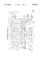
- FIG. 1 shows in block schematic form a processing device in accordance with the present invention
- FIG. 2 shows the format of a very long instruction word in the device of FIG. 1;
- FIG. 3 shows a part of the imitation multiport memory in the device of FIG. 1;
- FIG. 4 illustrates the operation of a first example program fragment
- FIG. 5 illustrates the scheduling of the first example program fragment for the device of FIG. 1, including the problem of collisions
- FIG. 6 shows a part of the processing device, including exception detection and recovery circuitry
- FIG. 7 shows in more detail a record/replay circuit of the processing device
- FIG. 8 illustrates the scheduling of a second example program fragment
- FIG. 9 illustrates the operation of the exception recovery circuitry in the execution of the second example program fragment.
- FIG. 10 shows in detail an alternative embodiment of the record/replay circuit of the processing device.
- the processing device of FIG. 1 comprises an imitation multiport memory circuit 30 which is connected to five functional units including a Constant Unit CO, an Arithmetic and Logic Unit AL, a Register Unit RG, a Data Memory Unit DM and a Branch Unit BR.
- memory circuit 30 there are shown in schematic form memory units 26, multiplexers 27 and a Special Register SP with an associated multiplexer 29.
- the principles of operation of such a memory circuit and processor are described in the copending parent application 594,534, and in the reference by Slavenburg and Labrousse, both mentioned above. These principles form no part of the present invention and their description has been omitted in the present application, for the sake of brevity.
- a Global Controller 41 which comprises a Sequencer SEQ and an Instruction Issue Pipeline IIP.
- the Sequencer SEQ generates in each cycle a program counter word PC which is supplied to Instruction Issue Pipeline IIP.
- the Instruction Issue Pipeline IIP may be off-chip, and includes the program memory wherein the very long instruction words forming the program for execution are encoded. After a certain number of cycles delay, Instruction Issue Pipeline IIP feeds an on-chip Instruction Register 46 with a very long instruction word IW stored in the program memory at the address PC.
- the instruction word IW in register 46 comprises a Destination Control field DEC and a number of fields COC, ALC, RGC, DMC and BRC for controlling the individual functional units CO, AL, RG, DM and BR respectively, and a further bit CP for checkpoint marking.
- the total number of bits in instruction word IW is 163, although the processor described is a very simple example.
- FIG. 2 shows fields of the instruction word IW in more detail, with the number of bits in each field marked beneath that field.
- the purpose of these various fields will become apparent from the following detailed description of the structure and operation of the processor.
- the purpose of the checkpoint marking bit CP will be described further below, with reference to FIGS. 6 to 10 of the drawings.
- Constant Unit CO has no operand inputs and one 32-bit result output (CO.O) connected to an input of memory circuit 30.
- Constant Unit CO in fact comprises a direct connection between the 32-bit field COC in instruction word IW (FIG. 2) and the output of Constant Unit CO.
- Constant Unit CO thereby enables constant values to be supplied from within the instruction word to the other units via the memory circuit 30.
- Arithmetic and Logic Unit AL has a 1-bit guard value input (AL.G) and two (left and right) 32-bit argument inputs (AL.L and AL.R) connected to respective memory units within memory circuit 30.
- the unit AL has a 32-bit output (AL.O) connected back into memory circuit 30, and is controlled by a 16-bit field ALC of instruction word IW.
- FIG. 3 shows in detail the part of the imitation multiport memory circuit 30 associated with Arithmetic and Logic Unit AL.
- separate memory units (RAM's) 48, 50 and 52 are associated with operands AL.G, AL.L and AL.R respectively.
- no separate write enable signals are provided for the memory units in the device of FIGS. 1 to 9. Instead, at least one non-existent or at least non-writable storage location can be addressed when writing to that memory unit is not desired.
- the width of instruction word IW is reduced by the absence of the write enable bits, on the assumption that the value of these bits is already known at the time of scheduling, when results are allocated to specific memory unit locations.
- the memory unit 48 for guard bit AL.G has eight 1-bit locations for storage of boolean values (TRUE/FALSE bits), including one non-writable location as just described.
- a 3-bit read address for memory unit 48 is supplied by Instruction Register 46 from a 3-bit field AL.G.RA in control field ALC of instruction word IW (see FIG. 2), and a 1-bit read port 54 of the memory unit supplies a guard bit AL.G to unit AL from the addressed memory location.
- a multiplexer 56 has a number of 1-bit inputs connected to the least significant bits (lsb's) of the 32-bit bus lines which are connected to the result outputs (CO.O, AL.O, etc.) of the various functional units.
- An additional input of the multiplexer is connected to the lsb of an additional 32-bit bus line 58, which carries a delayed result output SP.O from a delay element in the form of a Special Register SP.
- the provision and use of delay elements for resolving collisions in this type of VLIW processor forms the subject of the copending parent application 594,534 mentioned above.
- the use of the lsb for the guard bits affords compatibility with certain programming conventions, including for example those of the ⁇ C ⁇ language. In other environments the most significant bit (msb) or some other bit might be a more convenient choice.
- the multiplexer 56 has a 1-bit output 60 connected to a write port of memory unit 48.
- the multiplexer 56 is controlled by a 3-bit selection field AL.G.SE in the Destination Control field DEC of instruction word IW.
- a 3-bit write address for the write port of memory unit 48 is provided by the adjacent 3-bit field AL.G.WA in the Destination Control field DEC.
- 32-bit memory units 50 (for AL.L) and 52 (for AL.R) have associated 32-bit multiplexers 62 and 64 respectively. Each has 16 locations, including one non-writable location.
- Destination Control field DEC contains two 3-bit selection fields AL.L.SE and AL.R.SE for controlling multiplexers 62 and 64 and two 4-bit fields AL.L.WA and AL.R.WA providing 4-bit write port addresses for memory units 50 and 52 respectively.
- Two 4-bit fields AL.L.RA and AL.R.RA in control field ALC provide read addresses for the read ports of memory units 50 (for AL.L) and 52 (for AL.R) respectively.
- An op-code AL.OP for Arithmetic and Logic Unit AL is provided by a 5-bit field in control field ALC for unit AL.
- op-code AL.OP determines what operation (add, subtract, compare, AND, OR, etc.) is to be performed on the arguments AL.L and AL.R to generate the result AL.O.
- Register Unit RG provides on-chip storage for sixteen frequently used program variables of 32 bits each.
- the unit RG has associated memory units within memory circuit 30 for a guard bit RG.G and a 32-bit data input RG.I. These memory units have only four locations each, including one non-writable location.
- a data output (RG.O) is connected to an input of memory circuit 30 wherein it forms a respective bus line (RG.O, see also FIG. 3).
- Destination Control field DEC contains two 3-bit selection fields RG.G.SE and RG.I.SE for controlling the associated multiplexers and two 2-bit write address fields RG.G.WA and RG.I.WA for selecting between the four locations in the respective memory units.
- RG.G.RA and RG.I.RA are provided for selecting the location of the values RG.G and RG.I to be read from their respective memory units.
- a 5-bit op-code field RG.OP contains one bit to select between register read and register write functions, and four bits to select between the sixteen registers within unit RG. The location of a variable within Register Unit RG is therefore fixed by the compiler.
- Data Memory Unit DM contains, at least conceptually, a larger amount of storage for variables.
- Unit DM comprises in practice an interface to an off-chip bank of read/write memory, as described in more detail below, with reference to FIG. 6.
- DM.G Within the imitation multiport memory circuit 30, separate memory units are provided for a guard bit DM.G, a 32-bit address word DM.A and a 32-bit input data word DM.I. These memory units have 256 locations each, including one non-writable location.
- Data Memory Unit DM has a 32-bit data output (DM.O) connected to an input of memory circuit 30 wherein it forms a respective bus line (DM.O, see also FIG. 3).
- Destination Control field DEC contains three 3-bit selection fields DM.G.SE, DM.A.SE and DM.I.SE for controlling multiplexers within memory circuit 30, and three 8-bit write address fields DM.G.WA, DM.A.WA and DM.I.WA for selecting between the 256 locations in each of the associated memory units.
- DM.G.RA Within the 25-bit Data Memory Unit control field DMC, three 8-bit read addresses DM.G.RA, DM.A.RA and DM.I.RA are provided for selecting the location of the values DM.G, DM.A and DM.I to be read from their respective memory units.
- a 1-bit op-code field DM.OP contains one bit to select between memory read and memory write functions.
- the address word DM.A defines the address for the writing of data word DM.I or the reading of data word DM.O. This allows the dynamic calculation of 32-bit addresses during running of programs, enough to address 2 32 locations.
- Branch Unit BR allows the sequence of instruction addresses PC generated by Sequencer SEQ to be modified to cause branching in the program execution.
- the unit BR has associated memory units within memory circuit 30 for a guard bit BR.G and a 32-bit destination address BR.A. These memory units have four locations each including a non-writable location.
- Destination Control field DEC contains two 3-bit selection fields BR.G.SE and BR.A.SE for controlling the associated multiplexers and two 2-bit write address fields BR.G.WA and BR.A.WA for selecting between the four locations in the respective memory units.
- Branch Unit BR simply passes guard bit BR.G and destination address BR.A to the Sequencer SEQ. No op-code field BR.OP is required.
- Sequencer SEQ the boolean value of guard bit BR.G is tested. If BR.G is TRUE, then a branch is to be implemented and Sequencer SEQ makes the next value of PC equal to destination address BR.A received from memory circuit 30. If BR.G is FALSE, then Sequencer SEQ merely increments the value of PC to PC+1, addressing the next instruction in the stored program.
- conditional branching can be effected.
- Unconditional (always or never) branching can be effected by directing a constant result CO.O to the memory unit for BR.G, or by arranging that non-writable locations in that memory unit are permanently TRUE or permanently FALSE. This latter option is particularly convenient in the present embodiment, since at least one location in each memory unit is already non-writable, as described above.
- Sequencer SEQ also produces a pseudo-program counter value PPC which is fed to an input of memory circuit 30 wherein it forms a bus line (PPC, see FIG. 3).
- PPC can be used by other functional units, including Branch Unit BR, to implement program counter-relative addressing.
- a read delay may be defined as the difference between the cycle number of an instruction reading a value PPC from the bus line into a memory unit and the cycle number of the instruction with PC equal to that value of PPC.
- a branch delay of b cycles occurs between the cycle i in which a branch instruction is issued, and the first cycle i+b in which the instruction word IW(i+b) is affected by the branch instruction.
- the same boolean value which conditions the branch instruction can be directed to the guard bit inputs AL.G, RG.G, DM.G and BR.G and be used in the intervening cycles to conditionally inhibit state-changing operations scheduled for the various functional units during the branch delay, including further branches.
- the compiler is thereby enabled to schedule useful operations within the branch delay of an improbable conditional branch instruction, while ensuring a correct state in the minority of cases where the branch condition is met.
- each guard bit memory unit can be arranged to yield TRUE at its read port in response to the appropriate read addresses RA.
- the non-writable locations of the 32-bit operand memory units may also be arranged to yield some known, frequently required value, for example zero.
- the imitation multiport memory circuit 30 is used by the compiler as a buffer for intermediate variables on a strictly temporary basis. Consequently, functional units such as Constant Unit Co do not require guarding. Arithmetic and Logic Unit AL is provided with guarding to avoid exceptions such as arithmetic overflows arising spuriously, even though unit AL cannot itself alter the programmer-visible state of the device.
- the scheduling compiler In addition to the branch delay of Branch Unit BR, the scheduling compiler must have knowledge of the so-called ⁇ latency ⁇ of every functional unit.
- the latency of a functional unit is defined as the difference between the number of the cycle in which an operation is started and the number of the cycle in which the result (AL.O etc.) of that operation is produced and directed by Destination Control field DEC to the desired location(s) in the imitation multiport memory circuit 30.
- the branch delay mentioned above may be considered as the sum of the latency due to Branch Unit BR and a latency due to Sequencer SEQ and the off-chip Instruction Issue Pipeline IIP.
- Listing 1 comprises a fragment of high level language source code.
- Two records in memory are pointed to by variables p and q.
- the aim of the program is to cause copying of two 32-bit values from fields in the q record to two corresponding fields in the p record.
- FIG. 4 illustrates one possible organization of data that might be used to implement the high level instructions of Listing 1.
- Storage for program variables is provided by a high-speed register file REG, having sixteen locations numbered 0 to 15, and a larger bank MEM of (offchip) read/write memory.
- a Local Base address LB is stored in location 0 of register file REG.
- the address LB points to the start of a table of variable values in memory bank MEM, wherein the two record pointers p and q are stored at locations LB+12 and LB+8 respectively.
- Each variable p and q is a pointer to the start of the corresponding record, located elsewhere in memory bank MEM.
- the first field of each record is stored at an offset of zero from the address defined by the relevant pointer variable.
- the second field of each record is stored at an offset of four from the relevant pointer variable.
- the value q .field2 can be read from the location whose address is q 30 4.
- Listing 2 shows an intermediate code fragment, labelled T1, that might be generated by a compiler to execute the high level instructions of Listing 1 on a VLIW processor, assuming the data organization described above with reference to FIG. 4.
- Each line of Listing 2 defines a single primitive operation Op001 to Op014 to be scheduled for execution by a suitable functional unit.
- a comment (*. . . *) at the end of each line first mentions the type of functional unit required (AL, RG, CO etc.) and then describes the result (output) of that operation.
- the references 001 and 002 in operation Op003 indicate that the operands for Op003 are the results of Op001 and Op002 respectively.
- the intermediate code fragment T1 is listed sequentially, and is not specific to any particular configuration of VLIW processor, provided that at least one functional unit is suitable to perform each operation.
- the compiler Once the compiler has arrived at the collection of such fragments that make up an application program, and once the actual device configuration is known, it is the task of a scheduler to map each operation of the fragment to a particular functional unit of the device in a particular cycle.
- the scheduler operates with a set of constraints defined by the structure of the particular VLIW processor. These constraints include primarily the number and type of functional units available in the target VLIW processor, and the latency of each functional unit. Other constraints include the number of locations in each memory unit of the imitation multiport memory. These locations are allocated dynamically by the scheduler as required.
- each operation is important because operations dependent on the results of other operations must not be scheduled until the latencies of all those other operations have expired.
- operation Op009 must be scheduled at least 2 cycles later than Op004 (DM latency is 2) and at least 2 cycles later than Op008.
- operation Op011 can be scheduled in the same cycle as Op010 (CO latency is zero), but must be at least 2 cycles later than Op004 (DM latency is 2). This assumes that simultaneous write and read of a memory unit location is possible. Otherwise a further one cycle latency may be needed for each type of operation.
- FIG. 5 shows three different schedules (I, II and III), each mapping the intermediate code fragment T1 onto the specific VLIW processor described above with reference to FIGS. 1 to 4.
- Each row of each table represents one very long instruction word IW, and hence one machine cycle. Cycle numbers are given in the left-most column, headed Cy.
- the next five columns represent the five control fields COC, ALC, RGC, DMC and BRC for the five functional units (CO etc. in FIG. 1).
- Each control field begins an operation on its respective functional unit.
- the register reading operation Op001 is initiated in Cycle 0 by field RGC.
- the value LB of the Local Base address is thus RG.O in Cycle 1 (RG latency is 1).
- the selection fields DEC.--.-.SE of Destination Control field DEC in each instruction are represented to the right of the functional unit control fields. These fields direct the results of the various operations Op00114 Op014 into respective memory units as such results become available.
- the scheduler takes account of the latencies of the various functional units in defining Destination Control field DEC.
- result RG.O of register reading operation Op001 started by field RGC in Cycle 0 is directed to the left operand memory unit of Arithmetic and Logic Unit AL by field DEC.AL.L.SE in the following instruction, Cycle 1.
- Nw015 uses Constant Unit CO in Cycle 1 to define the target address for the branch, which is directed to the address memory unit of Branch Unit BR by setting selection field DEC.BR.A.SE to ⁇ CO ⁇ in Cycle 1.
- BRC branch control field
- the long branch delay of 5 cycles ensures that transfer of control to the target address does not occur until Cycle 8, after fragment T1 has completed. In other words, the branch operation has been brought forward in the schedule so that useful operations can be scheduled for execution during the branch delay.
- the Schedule I in FIG. 5 could have been executed by a VLIW machine having a true multiport memory, ignoring the Destination Control field DEC altogether.
- Schedule I contains a collision for access to a memory unit of the imitation multiport memory, and is thus not a valid mapping of operations Op001-Op014 onto the processor of FIGS. 1 to 4.
- result DM.O of Op004 is destined for the left operand memory unit (AL.L) of Arithmetic and Logic Unit AL and for the address memory unit (DM.A) of Data Memory Unit DM.
- result AL.O of Op012 is also destined for the address memory unit (DM.A) of Data Memory Unit DM.
- This collision is marked by the code XX in field DEC.DM.A.SE in Cycle 5, Schedule I.
- Schedule III represents the resolution of the example collision without backtracking, using the delay element in the form of Special Register SP, as described more fully in the copending parent application 594,534.
- the selection field DEC.SP.SE in Destination Control field DEC is shown at the right in Schedule III. It will be seen that the scheduling of operations Op001-Op014 and Nw015-Nw016 is almost identical to that of Schedule I (true multiport memory).
- Schedule III the collision in Cycle 5 between the two results destined for the DM.A memory unit is resolved by directing the result DM.O of Op004 in to the Special Register, that is by setting field DEC.SP.SE to ⁇ DM ⁇ in Destination Control field DEC.
- the field DEC.DM.A.SE is then set to ⁇ SP ⁇ in Cycle 6 to direct the delayed result of Op004 to the DM.A memory unit in time for it to be read by Data Memory Unit DM in Op009, Cycle 6.
- Substantial freedom is also available in choosing the number and type of functional units to be included. While each unit in the specific embodiment of FIG. 1 is specialized to some extent for performing a specific function or group a functions, groups of these functions could all be combined in a more general multi-purpose type of functional unit, for maximum flexibility in scheduling.
- a disadvantage of this type of unit is that it is desirable to have the same latency for all operations on a given unit, to allow full pipelining. This means that the faster operations (such as constant generation) must be slowed down to the speed of the slowest operations.
- more specialized functional unit types may also be useful in a given application, performing for example floating-point multiplication, barrel shifting or input/output functions.
- the same types of units as are used in conventional microprocessors are well suited or readily adaptable by the person skilled in the art for inclusion in a processing device according to the present invention.
- FIG. 6 shows the structure of a memory interface circuit suitable for use as the Data Memory Unit DM of the processing device of FIGS. 1 to 4.
- Signals DM.G guard bit
- DM.A address
- DM.I write data
- a Memory Management Unit receives these signal via some exception recovery circuitry 100 (not shown in FIG. 1), and supplies signal DM.O (read data) to memory circuit 30, also via the circuitry 100.
- the op-code signal DM.OP read/write
- the MMU provides an interface to a large off-chip main memory MEM, and in particular implements virtual memory addressing in a manner familiar per se to those skilled in the art.
- the signals DM.A and DM.I are unaffected, while the guard bit DM.G is AND-ed with a guard forcing signal GF before being passed as signal DM.G' to the MMU. While signal GF remains at logic ⁇ 1 ⁇ (TRUE), signal DM.G' equals signal DM.G. When signal GF goes to logic ⁇ 0 ⁇ (FALSE), however, DM.G' is forced to ⁇ 0 ⁇ (FALSE).
- the guard forcing signal GF is ANDed in a similar manner (not shown) with the guard bits AL.G, RG.G and BR.G of the other functional units in the processing device of FIG. 1.
- the exception recovery circuitry 100 also includes a multiplexer 102 and record/replay circuit RRC.
- the circuit RRC controls the multiplexer 102 by means of a replay mode signal REP. While REP is at logic ⁇ 0 ⁇ , the multiplexer transmits signal DM.O', produced by the MMU, to the imitation multiport memory circuit 30 as signal DM.O. When REP is at ⁇ 1 ⁇ , however, a replay data signal DREP, produced by record/replay circuit RRC, is transmitted to memory circuit 30 in place of DM.O'.
- the MMU also supplies a TLB miss signal TLBM, to be described below, to an input of an OR gate 104, whose output carries an exception detection signal EXDET to the Sequencer SEQ and Instruction Issue Pipeline IIP (see FIG. 1).
- OR gate 104 whose output carries an exception detection signal EXDET to the Sequencer SEQ and Instruction Issue Pipeline IIP (see FIG. 1).
- Other inputs of the OR gate 104 are available to receive exception raising signals from other functional units.
- Signal EXDET is also applied to the reset (R) input of a set-reset flip flop 106, which is clocked once every machine cycle.
- the Instruction Issue Pipeline IIP generates and supplies to the record/replay circuit RRC an exception handling signal EXH and a checkpoint signal CPT.
- the exception handling signal EXH is also applied to the set (S) input of flip flop 106, while the output signal (Q) of the flip flop 106 constitutes the guard forcing signal GF.
- FIG. 7 shows the record/replay circuit RRC in more detail.
- a time counter TIC clocked once every machine cycle, receives the checkpoint signal CPT and generates a time signal TREC.
- the time signal TREC is applied in concatenation with the signal DREC to a data input (DIN) of an event memory EVM. Since the signal DM.O has 32 bits, and assuming a width of 8 bits for the time signal TREC, the data input of the event memory EVM has a width of 40 bits.
- Time signal TREC is also supplied to an event counter logic circuit EVC, as are the checkpoint signal CPT, the event signal EVT and the exception handling signal EXH.
- the logic circuit EVC controls the event memory EVM by means of address and write enable signals ADDR and WE respectively.
- the event memory EVM has a 40-bit data output DOUT, out of which an 8-bit event time signal TREP and a 32-bit replay data signal are applied to the logic circuit EVC and a latch 108 respectively.
- the latch 108 is clocked by a next event signal NXT supplied by the logic circuit EVC, while the latch output supplies the replay data signal DREP to the multiplexer 102.
- MMU of this embodiment contains a Translation Lookaside Buffer (TB or TLB), which in turn contains a number of entries mapping virtual addresses (DM.A) to physical addresses in the memory MEM. Only a subset of the possible addresses can be mapped by the TLB at a given time, and a request for a read or write to an address DM.A can only be met within the Data Memory Unit latency (2 cycles in the present embodiment) if it can be mapped by an entry existing in the TLB. If the address DM.A cannot be mapped by an existing entry, this constitutes an exception, and the program execution must be interrupted.
- TLB Translation Lookaside Buffer
- DM.A mapping virtual addresses
- TLB miss can be resolved by making a new TLB entry (deleting an existing entry), the TLB miss is termed a ⁇ non-fatal ⁇ or ⁇ recoverable ⁇ exception.
- the fragment deliberately makes no use of values already present in the imitation multiport memory circuit 30.
- a pointer to the relevant memory location is stored in register 0 of the Register Unit RG.
- signals CPT, EVT, EXDET, EXH and REP are all at ⁇ 0 ⁇ , and GF is at ⁇ 1 ⁇ , indicating normal operation (record mode, no exceptions being handled).
- the time counter signal TREC is counting cycles since the previous checkpoint (not shown).
- the time count signal TREC is incremented in each subsequent cycle to act as a measure of time elapsed since the checkpoint.
- These two cycles 0 allow any operations initiated before the exception, including for example the operation ⁇ write t1 t4 ⁇ , to complete their execution.
- These and other operations initiated before the exception is detected have therefore altered the machine state from the well-defined state that was present at the checkpoint.
- the exception handling routine operates with a small area of memory which is permanently and directly addressable. By this means, and appropriate programming, it is guaranteed that the exception handling routine will never itself give rise to a non-fatal exception. This measure is known per se to the person skilled in the art, for example from the reference Colwell et al cited above.
- the operations required of the exception handling routine are dependent on the MMU, in a manner well known to those skilled in the art, and further description of these is not needed for an understanding of the exception recovery process being described herein.
- exception handling may also be performed by special hardware, without explicit provision by the programmer. In 680 ⁇ 0 processors, for example, special ⁇ table walk ⁇ hardware is provided to handle the TLB miss exception.
- the checkpoint signal CPT is set in time for this cycle, in response to which time counter TIC in the record/replay circuit RRC resets time signal TREC to zero and begins counting cycles again from the checkpoint.
- the multiplexer 102 therefore breaks the data path for the signal DM.O', supplied by the MMU, and substitutes the replay data signal DREP, produced from event memory EVM via latch 108.
- circuit EVC detects equality between the current time signal TREC and the stored time stamp TREP, and uses signal NXT to enter the value recorded at time E in the original execution into latch 108.
- the value DM.O supplied to the imitation multiport memory circuit 30 at time T' is the value that was originally in the memory MEM at time T, and not the incremented value that was stored there by the operation ⁇ write t1 t4 ⁇ in the original execution of the program fragment.
- a number of data memory units DM may be provided, enabling multiple accesses to the main memory MEM in each cycle.
- a record/replay circuit will be required for each data path from the main memory MEM.
- Some elements of the circuit RRC, for example the time counter TIC, can be shared between two or more such circuits, since the entire processing device operates synchronously.
- these further memory units will ideally provide additional ports to the same main memory space MEM, rather than to further isolated memories, in order to increase the scope for parallel processing.
- Register Unit RG Since the Register Unit RG also contains programmer-visible machine state, it too is provided with exception recovery features. However, since the amount of state in unit RG is very small, backup copy registers are used to store the state at each checkpoint, in the conventional manner, as described for example by Hwu and Patt in the reference cited above. The exception recovery features of the Register Unit will therefore not be described further, in the interest of brevity. Those skilled in the art will appreciate that, as an alternative, the (or each) Register Unit output data path (RG.O) could include a record/replay circuit, for example if the number of registers is too large for complete backup copies to be accommodated economically.
- the content of the imitation multiport memory itself could be included in the definition of the machine state, in which case each memory unit (26, FIG. 1) would be provide with exception recovery features in the form of a backup memory unit or a record/replay circuit, depending on the size of the memory unit in question.
- FIG. 10 shows an alternative embodiment of the record/replay circuit of FIG. 7, in which the time counter TIC is not provided, and time stamp values (TREC) are not stored with the data entries in the event memory EVM.
- TRC time stamp values
- the record/replay circuit provides effectively a ⁇ first-in, first-out ⁇ or FIFO memory which, during record mode, stores a new value DREC whenever the event signal EVT is asserted, and during replay mode reproduces a next stored value DREP when the event signal is asserted.
- event memory control circuit EVC still maintains a count of the number of values actually recorded since the checkpoint, in order to generate address ADDR, and to effect the changeover from replay to record mode when the re-execution passes the point at which the exception interrupted it at the previous attempt.
- the system designer also has to ensure that the starting value of address ADDR, and the number of assertions of event signal EVT, correspond exactly in both record and replay mode, or the replay values will no longer reproduce the correct recorded values.
- an op-code (--.OP) issued at PC i+1
- the guarding mechanism of the device described herein allows a clear answer to this question, thereby allowing the designer to eliminate control pipelining.
- each pending operation must be considered completed if and only if the guard selection field for that operation was issued before the exception was detected and the guard forcing signal GF became active.
- the time at which the other fields are issued is then a matter for the designer of the device and its scheduling compiler to determine, with freedom to eliminate control pipelining.
Abstract
Description
 ______________________________________
Listing 2
______________________________________
T1:
Op001    rdreg(0);   (* RG, Local Base address *)
Op002    constant(12);
                     (* CO, offset value for p *)
Op003    aplus 001 002;
                     (* AL, address of p *)
Op004    read 003;   (* DM, p *)
Opo05    constant(8);
                     (* CO, offset value for q *)
Op006    aplus 001 005;
                     (* AL, address of q *)
Op007    read 006;      (* DM, q *)
Op008    read 007;   (* DM, q .field1 *)
Op009    write 004 008;
                     (* DM, p .field1 := q .field1 *)
Op010    constant(4);
                     (* CO, offset for field2 *)
Op011    aplus 004 010;
                     (* AL, address of p .field2 *)
Op012    aplus 007 010;
                     (* AL, address of q .field2 *)
Op013    read 012;   (* DM, q .field2 *)
Op014    write 011 013;
                     (* DN, p .field2 := q .field2 *)
GOTO EXIT
______________________________________
Claims (23)
Priority Applications (6)
| Application Number | Priority Date | Filing Date | Title |
|---|---|---|---|
| US08/358,127 US5832202A (en) | 1988-12-28 | 1994-12-16 | Exception recovery in a data processing system |
| EP95936065A EP0745241B1 (en) | 1994-12-16 | 1995-11-21 | Exception recovery in a data processing system |
| DE69527705T DE69527705D1 (en) | 1994-12-16 | 1995-11-21 | RECOVERY FUNCTION CORRECTION FOR A DATA PROCESSING SYSTEM |
| JP8518521A JPH09509515A (en) | 1994-12-16 | 1995-11-21 | Data processing system exception recovery |
| KR1019960704551A KR970701391A (en) | 1994-12-16 | 1995-11-21 | Exception recovery in a data processing system |
| PCT/IB1995/001030 WO1996018950A2 (en) | 1994-12-16 | 1995-11-21 | Exception recovery in a data processing system |
Applications Claiming Priority (6)
| Application Number | Priority Date | Filing Date | Title |
|---|---|---|---|
| US29097988A | 1988-12-28 | 1988-12-28 | |
| US57897690A | 1990-09-15 | 1990-09-15 | |
| US59453490A | 1990-10-05 | 1990-10-05 | |
| US65484792A | 1992-02-11 | 1992-02-11 | |
| US99808092A | 1992-12-29 | 1992-12-29 | |
| US08/358,127 US5832202A (en) | 1988-12-28 | 1994-12-16 | Exception recovery in a data processing system |
Related Parent Applications (1)
| Application Number | Title | Priority Date | Filing Date |
|---|---|---|---|
| US99808092A Continuation-In-Part | 1988-12-28 | 1992-12-29 |
Publications (1)
| Publication Number | Publication Date |
|---|---|
| US5832202A true US5832202A (en) | 1998-11-03 |
Family
ID=23408416
Family Applications (1)
| Application Number | Title | Priority Date | Filing Date |
|---|---|---|---|
| US08/358,127 Expired - Lifetime US5832202A (en) | 1988-12-28 | 1994-12-16 | Exception recovery in a data processing system |
Country Status (6)
| Country | Link |
|---|---|
| US (1) | US5832202A (en) |
| EP (1) | EP0745241B1 (en) |
| JP (1) | JPH09509515A (en) |
| KR (1) | KR970701391A (en) |
| DE (1) | DE69527705D1 (en) |
| WO (1) | WO1996018950A2 (en) |
Cited By (16)
| Publication number | Priority date | Publication date | Assignee | Title |
|---|---|---|---|---|
| US20030055928A1 (en) * | 2001-09-03 | 2003-03-20 | Nec Corporation | Automatic computer configuration system, method and program making use of portable terminal |
| US6622263B1 (en) * | 1999-06-30 | 2003-09-16 | Jack Justin Stiffler | Method and apparatus for achieving system-directed checkpointing without specialized hardware assistance |
| US20040025148A1 (en) * | 2002-08-01 | 2004-02-05 | Krueger Steven E. | Computer-implemented system and method for code generation |
| US20040025084A1 (en) * | 2002-08-01 | 2004-02-05 | Krueger Steven E. | Computer-implemented exception handling system and method |
| US20050132170A1 (en) * | 2002-04-18 | 2005-06-16 | Koninklijke Philips Electroncis N.C. | Multi-issue processor |
| US20050187750A1 (en) * | 2004-02-25 | 2005-08-25 | Fujitsu Limited | Data processing device designing method, data processing device designing apparatus, program and computer readable information recording medium |
| US7386752B1 (en) * | 2004-06-30 | 2008-06-10 | Symantec Operating Corporation | Using asset dependencies to identify the recovery set and optionally automate and/or optimize the recovery |
| US20080313440A1 (en) * | 2000-03-30 | 2008-12-18 | Transmeta Corporation | Switching to original code comparison of modifiable code for translated code validity when frequency of detecting memory overwrites exceeds threshold |
| US20090292908A1 (en) * | 2008-05-23 | 2009-11-26 | On Demand Electronics | Method and arrangements for multipath instruction processing |
| US7685403B1 (en) | 1999-10-20 | 2010-03-23 | Brett Coon | Pipeline replay support for multi-cycle operations |
| US7761857B1 (en) | 1999-10-13 | 2010-07-20 | Robert Bedichek | Method for switching between interpretation and dynamic translation in a processor system based upon code sequence execution counts |
| US7886135B1 (en) * | 1999-10-20 | 2011-02-08 | Brett Coon | Pipeline replay support for unaligned memory operations |
| US8019983B1 (en) * | 2003-04-02 | 2011-09-13 | Rozas Guillermo J | Setting a flag bit to defer event handling to a safe point in an instruction stream |
| EP2472392A1 (en) * | 2010-12-29 | 2012-07-04 | Fujitsu Limited | Processing apparatus and method for performing computation |
| US8413162B1 (en) | 2005-06-28 | 2013-04-02 | Guillermo J. Rozas | Multi-threading based on rollback |
| US20170185408A1 (en) * | 2015-12-28 | 2017-06-29 | Qualcomm Incorporated | Replay of partially executed instruction blocks in a processor-based system employing a block-atomic execution model |
Families Citing this family (1)
| Publication number | Priority date | Publication date | Assignee | Title |
|---|---|---|---|---|
| US9626313B2 (en) | 2014-12-18 | 2017-04-18 | Qualcomm Incorporated | Trace buffer based replay for context switching |
Citations (11)
| Publication number | Priority date | Publication date | Assignee | Title |
|---|---|---|---|---|
| US3736566A (en) * | 1971-08-18 | 1973-05-29 | Ibm | Central processing unit with hardware controlled checkpoint and retry facilities |
| EP0163096A1 (en) * | 1984-04-26 | 1985-12-04 | BBC Brown Boveri AG | Apparatus for saving a calculator status |
| EP0212132A1 (en) * | 1985-06-28 | 1987-03-04 | Hewlett-Packard Company | Method and digital computer for recovering from errors |
| US4703481A (en) * | 1985-08-16 | 1987-10-27 | Hewlett-Packard Company | Method and apparatus for fault recovery within a computing system |
| US4740969A (en) * | 1986-06-27 | 1988-04-26 | Hewlett-Packard Company | Method and apparatus for recovering from hardware faults |
| US4875160A (en) * | 1988-07-20 | 1989-10-17 | Digital Equipment Corporation | Method for implementing synchronous pipeline exception recovery |
| EP0348652A2 (en) * | 1988-06-30 | 1990-01-03 | International Business Machines Corporation | Checkpoint retry system |
| US4941087A (en) * | 1986-09-19 | 1990-07-10 | Asea Aktiebolag | System for bumpless changeover between active units and backup units by establishing rollback points and logging write and read operations |
| US5003458A (en) * | 1986-10-24 | 1991-03-26 | Hitachi, Ltd. | Suspended instruction restart processing system based on a checkpoint microprogram address |
| US5313551A (en) * | 1988-12-28 | 1994-05-17 | North American Philips Corporation | Multiport memory bypass under software control |
| US5450556A (en) * | 1990-09-05 | 1995-09-12 | North American Philips Corporation | VLIW processor which uses path information generated by a branch control unit to inhibit operations which are not on a correct path |
-
1994
- 1994-12-16 US US08/358,127 patent/US5832202A/en not_active Expired - Lifetime
-
1995
- 1995-11-21 KR KR1019960704551A patent/KR970701391A/en not_active Application Discontinuation
- 1995-11-21 WO PCT/IB1995/001030 patent/WO1996018950A2/en active IP Right Grant
- 1995-11-21 EP EP95936065A patent/EP0745241B1/en not_active Expired - Lifetime
- 1995-11-21 JP JP8518521A patent/JPH09509515A/en active Pending
- 1995-11-21 DE DE69527705T patent/DE69527705D1/en not_active Expired - Lifetime
Patent Citations (11)
| Publication number | Priority date | Publication date | Assignee | Title |
|---|---|---|---|---|
| US3736566A (en) * | 1971-08-18 | 1973-05-29 | Ibm | Central processing unit with hardware controlled checkpoint and retry facilities |
| EP0163096A1 (en) * | 1984-04-26 | 1985-12-04 | BBC Brown Boveri AG | Apparatus for saving a calculator status |
| EP0212132A1 (en) * | 1985-06-28 | 1987-03-04 | Hewlett-Packard Company | Method and digital computer for recovering from errors |
| US4703481A (en) * | 1985-08-16 | 1987-10-27 | Hewlett-Packard Company | Method and apparatus for fault recovery within a computing system |
| US4740969A (en) * | 1986-06-27 | 1988-04-26 | Hewlett-Packard Company | Method and apparatus for recovering from hardware faults |
| US4941087A (en) * | 1986-09-19 | 1990-07-10 | Asea Aktiebolag | System for bumpless changeover between active units and backup units by establishing rollback points and logging write and read operations |
| US5003458A (en) * | 1986-10-24 | 1991-03-26 | Hitachi, Ltd. | Suspended instruction restart processing system based on a checkpoint microprogram address |
| EP0348652A2 (en) * | 1988-06-30 | 1990-01-03 | International Business Machines Corporation | Checkpoint retry system |
| US4875160A (en) * | 1988-07-20 | 1989-10-17 | Digital Equipment Corporation | Method for implementing synchronous pipeline exception recovery |
| US5313551A (en) * | 1988-12-28 | 1994-05-17 | North American Philips Corporation | Multiport memory bypass under software control |
| US5450556A (en) * | 1990-09-05 | 1995-09-12 | North American Philips Corporation | VLIW processor which uses path information generated by a branch control unit to inhibit operations which are not on a correct path |
Non-Patent Citations (12)
| Title |
|---|
| "A VLIW Architecture for a Trace Scheduling Compiler", by R.P. Colwell et al, pp. 180-192. |
| "Checkpoint Repair for High-Performance Out-of-Order Execution Machines", by W. Wen-Mei et al, IEEE 1987, pp. 1496-1514. |
| "Intel Microprocessors, vol. I". |
| "MC68020 32-Bit Microprocessor User's Manual", Motorola. |
| "The SPARC Architecture Manual", Version 8. |
| A VLIW Architecture for a Trace Scheduling Compiler , by R.P. Colwell et al, pp. 180 192. * |
| Alexander et al., "Contributions: Translation Buffer Performance in a UNIX Environment", Computer Architecture News, vol. 13, No. 5, Dec. 1985, pp. 1-14. |
| Alexander et al., Contributions: Translation Buffer Performance in a UNIX Environment , Computer Architecture News, vol. 13, No. 5, Dec. 1985, pp. 1 14. * |
| Checkpoint Repair for High Performance Out of Order Execution Machines , by W. Wen Mei et al, IEEE 1987, pp. 1496 1514. * |
| Intel Microprocessors, vol. I . * |
| MC68020 32 Bit Microprocessor User s Manual , Motorola. * |
| The SPARC Architecture Manual , Version 8. * |
Cited By (34)
| Publication number | Priority date | Publication date | Assignee | Title |
|---|---|---|---|---|
| US6622263B1 (en) * | 1999-06-30 | 2003-09-16 | Jack Justin Stiffler | Method and apparatus for achieving system-directed checkpointing without specialized hardware assistance |
| US7761857B1 (en) | 1999-10-13 | 2010-07-20 | Robert Bedichek | Method for switching between interpretation and dynamic translation in a processor system based upon code sequence execution counts |
| US8418153B2 (en) | 1999-10-13 | 2013-04-09 | Robert Bedichek | Method for integration of interpretation and translation in a microprocessor |
| US20100262955A1 (en) * | 1999-10-13 | 2010-10-14 | Robert Bedichek | Method for integration of interpretation and translation in a microprocessor |
| US7886135B1 (en) * | 1999-10-20 | 2011-02-08 | Brett Coon | Pipeline replay support for unaligned memory operations |
| US7685403B1 (en) | 1999-10-20 | 2010-03-23 | Brett Coon | Pipeline replay support for multi-cycle operations |
| US8117423B1 (en) | 1999-10-20 | 2012-02-14 | Brett Coon | Pipeline replay support for multicycle operations |
| US8516224B2 (en) | 1999-10-20 | 2013-08-20 | Brett Coon | Pipeline replay support for multicycle operations |
| US7904891B2 (en) | 2000-03-30 | 2011-03-08 | John Banning | Checking for instruction invariance to execute previously obtained translation code by comparing instruction to a copy stored when write operation to the memory portion occur |
| US8438548B2 (en) | 2000-03-30 | 2013-05-07 | John Banning | Consistency checking of source instruction to execute previously translated instructions between copy made upon occurrence of write operation to memory and current version |
| US20080313440A1 (en) * | 2000-03-30 | 2008-12-18 | Transmeta Corporation | Switching to original code comparison of modifiable code for translated code validity when frequency of detecting memory overwrites exceeds threshold |
| US7191324B2 (en) * | 2001-09-03 | 2007-03-13 | Nec Corporation | Automatic computer configuration system, method and program making use of portable terminal |
| US20030055928A1 (en) * | 2001-09-03 | 2003-03-20 | Nec Corporation | Automatic computer configuration system, method and program making use of portable terminal |
| US20050132170A1 (en) * | 2002-04-18 | 2005-06-16 | Koninklijke Philips Electroncis N.C. | Multi-issue processor |
| US8095780B2 (en) | 2002-04-18 | 2012-01-10 | Nytell Software LLC | Register systems and methods for a multi-issue processor |
| US20040025084A1 (en) * | 2002-08-01 | 2004-02-05 | Krueger Steven E. | Computer-implemented exception handling system and method |
| US20040025148A1 (en) * | 2002-08-01 | 2004-02-05 | Krueger Steven E. | Computer-implemented system and method for code generation |
| US7320121B2 (en) | 2002-08-01 | 2008-01-15 | Sas Institute Inc. | Computer-implemented system and method for generating embedded code to add functionality to a user application |
| US7003762B2 (en) * | 2002-08-01 | 2006-02-21 | Sas Institute Inc. | Computer-implemented exception handling system and method |
| US8464033B2 (en) | 2003-04-02 | 2013-06-11 | Guillermo J. Rozas | Setting a flag bit to defer event handling to one of multiple safe points in an instruction stream |
| US8019983B1 (en) * | 2003-04-02 | 2011-09-13 | Rozas Guillermo J | Setting a flag bit to defer event handling to a safe point in an instruction stream |
| US7447617B2 (en) * | 2004-02-25 | 2008-11-04 | Fujitsu Limited | Data processing device designing method, data processing device designing apparatus, program and computer readable information recording medium |
| US20050187750A1 (en) * | 2004-02-25 | 2005-08-25 | Fujitsu Limited | Data processing device designing method, data processing device designing apparatus, program and computer readable information recording medium |
| US8015430B1 (en) | 2004-06-30 | 2011-09-06 | Symantec Operating Corporation | Using asset dependencies to identify the recovery set and optionally automate and/or optimize the recovery |
| US7386752B1 (en) * | 2004-06-30 | 2008-06-10 | Symantec Operating Corporation | Using asset dependencies to identify the recovery set and optionally automate and/or optimize the recovery |
| US8413162B1 (en) | 2005-06-28 | 2013-04-02 | Guillermo J. Rozas | Multi-threading based on rollback |
| US20090292908A1 (en) * | 2008-05-23 | 2009-11-26 | On Demand Electronics | Method and arrangements for multipath instruction processing |
| EP2472392A1 (en) * | 2010-12-29 | 2012-07-04 | Fujitsu Limited | Processing apparatus and method for performing computation |
| US9043581B2 (en) | 2010-12-29 | 2015-05-26 | Fujitsu Limited | Storing in other queue when reservation station instruction queue reserved for immediate source operand instruction execution unit is full |
| US20170185408A1 (en) * | 2015-12-28 | 2017-06-29 | Qualcomm Incorporated | Replay of partially executed instruction blocks in a processor-based system employing a block-atomic execution model |
| WO2017116652A1 (en) * | 2015-12-28 | 2017-07-06 | Qualcomm Incorporated | Replay of partially executed instruction blocks in a processor-based system employing a block-atomic execution model |
| CN108369519A (en) * | 2015-12-28 | 2018-08-03 | 高通股份有限公司 | The instruction block that replayed portion executes in the processor-based system for executing model using block-atom |
| US11188336B2 (en) | 2015-12-28 | 2021-11-30 | Qualcomm Incorporated | Replay of partially executed instruction blocks in a processor-based system employing a block-atomic execution model |
| AU2016380796B2 (en) * | 2015-12-28 | 2021-12-16 | Qualcomm Incorporated | Replay of partially executed instruction blocks in a processor-based system employing a block-atomic execution model |
Also Published As
| Publication number | Publication date |
|---|---|
| KR970701391A (en) | 1997-03-17 |
| EP0745241B1 (en) | 2002-08-07 |
| EP0745241A1 (en) | 1996-12-04 |
| WO1996018950A3 (en) | 1996-08-22 |
| DE69527705D1 (en) | 2002-09-12 |
| WO1996018950A2 (en) | 1996-06-20 |
| JPH09509515A (en) | 1997-09-22 |
Similar Documents
| Publication | Publication Date | Title |
|---|---|---|
| US5313551A (en) | Multiport memory bypass under software control | |
| US5832202A (en) | Exception recovery in a data processing system | |
| JP3984786B2 (en) | Scheduling instructions with different latency | |
| US5467473A (en) | Out of order instruction load and store comparison | |
| EP0479390B1 (en) | Processing device including a memory circuit and a group of functional units | |
| US6189088B1 (en) | Forwarding stored dara fetched for out-of-order load/read operation to over-taken operation read-accessing same memory location | |
| US5692139A (en) | VLIW processing device including improved memory for avoiding collisions without an excessive number of ports | |
| US5450560A (en) | Pointer for use with a buffer and method of operation | |
| US5630157A (en) | Computer organization for multiple and out-of-order execution of condition code testing and setting instructions | |
| US6839832B2 (en) | Register file backup queue | |
| US5341482A (en) | Method for synchronization of arithmetic exceptions in central processing units having pipelined execution units simultaneously executing instructions | |
| US6330661B1 (en) | Reducing inherited logical to physical register mapping information between tasks in multithread system using register group identifier | |
| US5694565A (en) | Method and device for early deallocation of resources during load/store multiple operations to allow simultaneous dispatch/execution of subsequent instructions | |
| RU2142157C1 (en) | Method for operations of processing system | |
| US6301654B1 (en) | System and method for permitting out-of-order execution of load and store instructions | |
| US5479622A (en) | Single cycle dispatch delay in a multiple instruction dispatch mechanism of a data processing system | |
| US5504925A (en) | Apparatus and method for implementing interrupts in pipelined processors | |
| EP0354585B1 (en) | Instruction pipeline microprocessor | |
| EP0518420A2 (en) | Computer system for concurrent processing of multiple out-of-order instructions | |
| KR100322632B1 (en) | Data cache with data storage and tag logic with different clocks | |
| US5694553A (en) | Method and apparatus for determining the dispatch readiness of buffered load operations in a processor | |
| US5907693A (en) | Autonomously cycling data processing architecture | |
| US5678016A (en) | Processor and method for managing execution of an instruction which determine subsequent to dispatch if an instruction is subject to serialization | |
| US5784606A (en) | Method and system in a superscalar data processing system for the efficient handling of exceptions | |
| EP0762271A2 (en) | Early completion of floating-point operations during load/store multiple operations |
Legal Events
| Date | Code | Title | Description |
|---|---|---|---|
| AS | Assignment |
Owner name: PHILIPS ELECTRONICS NORTH AMERICA CORPORATION, NEW Free format text: ASSIGNMENT OF ASSIGNORS INTEREST;ASSIGNORS:SLAVENBURG, GERRIT ARY;LABROUSSE, JUNIEN;REEL/FRAME:007385/0222 Effective date: 19950308 |
|
| STCF | Information on status: patent grant |
Free format text: PATENTED CASE |
|
| AS | Assignment |
Owner name: TRIMEDIA TECHNOLOGIES, CALIFORNIA Free format text: ASSIGNMENT OF ASSIGNORS INTEREST;ASSIGNOR:PHILIPS ELECTRONICS NORTH AMERICA CORPORATION;REEL/FRAME:010958/0776 Effective date: 20000628 |
|
| FEPP | Fee payment procedure |
Free format text: PAYOR NUMBER ASSIGNED (ORIGINAL EVENT CODE: ASPN); ENTITY STATUS OF PATENT OWNER: LARGE ENTITY |
|
| FPAY | Fee payment |
Year of fee payment: 4 |
|
| REMI | Maintenance fee reminder mailed | ||
| FPAY | Fee payment |
Year of fee payment: 8 |
|
| AS | Assignment |
Owner name: NXP B.V., NETHERLANDS Free format text: ASSIGNMENT OF ASSIGNORS INTEREST;ASSIGNOR:PHILIPS SEMICONDUCTORS INC.;REEL/FRAME:018635/0972 Effective date: 20061206 Owner name: PHILIPS SEMICONDUCTORS INC., NEW YORK Free format text: MERGER;ASSIGNOR:TRIMEDIA TECHNOLOGIES, INC.;REEL/FRAME:018635/0857 Effective date: 20040315 |
|
| FPAY | Fee payment |
Year of fee payment: 12 |
|
| FEPP | Fee payment procedure |
Free format text: PAYOR NUMBER ASSIGNED (ORIGINAL EVENT CODE: ASPN); ENTITY STATUS OF PATENT OWNER: LARGE ENTITY Free format text: PAYER NUMBER DE-ASSIGNED (ORIGINAL EVENT CODE: RMPN); ENTITY STATUS OF PATENT OWNER: LARGE ENTITY |
|
| AS | Assignment |
Owner name: TRIMEDIA TECHNOLOGIES, INC., CALIFORNIA Free format text: CORRECTION TO THE RECORDATION COVER SHEET OF THE ASSIGNMENT RECORDED AT 010958/0776 ON 07/10/2000; NAME AND ADDRESS OF RECEIVING PARTY CHANGED FROM TRIMEDIA TECHNOLOGIES TO TRIMEDIA TECHNOLOGIES, INC;ASSIGNOR:PHILIPS ELECTRONICS NORTH AMERICA CORPORATION;REEL/FRAME:026443/0748 Effective date: 20110511 Owner name: TRIMEDIA TECHNOLOGIES, INC., CALIFORNIA Free format text: CORRECTION TO THE RECORDATION COVER SHEET OF THE ASSIGNMENT RECORDED AT 010958/0776 ON 7/10/2000;NAME AND ADDRESS OF RECEIVING PARTY CHANGED FROM TRIMEDIA TECHNOLOGIES TO TRIMEDIA TECHNOLOGY,INC;ASSIGNOR:PHILIPS ELECTRONICS NORTH AMERICA CORPORATION;REEL/FRAME:026444/0646 Effective date: 20000628 |
|
| AS | Assignment |
Owner name: NXP B.V., NETHERLANDS Free format text: CONFIRMATORY ASSIGNMENT;ASSIGNOR:PHILIPS SEMICONDUCTORS INC.;REEL/FRAME:026365/0731 Effective date: 20110531 |
|
| AS | Assignment |
Owner name: NYTELL SOFTWARE LLC, DELAWARE Free format text: ASSIGNMENT OF ASSIGNORS INTEREST;ASSIGNOR:NXP B.V.;REEL/FRAME:026634/0532 Effective date: 20110628 |
|
| AS | Assignment |
Owner name: HANGER SOLUTIONS, LLC, GEORGIA Free format text: ASSIGNMENT OF ASSIGNORS INTEREST;ASSIGNOR:INTELLECTUAL VENTURES ASSETS 158 LLC;REEL/FRAME:051486/0425 Effective date: 20191206 |
|
| AS | Assignment |
Owner name: INTELLECTUAL VENTURES ASSETS 158 LLC, DELAWARE Free format text: ASSIGNMENT OF ASSIGNORS INTEREST;ASSIGNOR:NYTELL SOFTWARE LLC;REEL/FRAME:051777/0173 Effective date: 20191126 |
|
| AS | Assignment |
Owner name: FOOTHILLS IP LLC, COLORADO Free format text: ASSIGNMENT OF ASSIGNORS INTEREST;ASSIGNOR:HANGER SOLUTIONS, LLC;REEL/FRAME:056246/0533 Effective date: 20200515 |