US5835212A - Variable chirp optical modulator using single modulation source - Google Patents
Variable chirp optical modulator using single modulation source Download PDFInfo
- Publication number
- US5835212A US5835212A US08/731,760 US73176096A US5835212A US 5835212 A US5835212 A US 5835212A US 73176096 A US73176096 A US 73176096A US 5835212 A US5835212 A US 5835212A
- Authority
- US
- United States
- Prior art keywords
- optical
- interferometer
- modulation
- signals
- optical signals
- Prior art date
- Legal status (The legal status is an assumption and is not a legal conclusion. Google has not performed a legal analysis and makes no representation as to the accuracy of the status listed.)
- Expired - Fee Related
Links
Images


Classifications
-
- G—PHYSICS
- G02—OPTICS
- G02F—OPTICAL DEVICES OR ARRANGEMENTS FOR THE CONTROL OF LIGHT BY MODIFICATION OF THE OPTICAL PROPERTIES OF THE MEDIA OF THE ELEMENTS INVOLVED THEREIN; NON-LINEAR OPTICS; FREQUENCY-CHANGING OF LIGHT; OPTICAL LOGIC ELEMENTS; OPTICAL ANALOGUE/DIGITAL CONVERTERS
- G02F1/00—Devices or arrangements for the control of the intensity, colour, phase, polarisation or direction of light arriving from an independent light source, e.g. switching, gating or modulating; Non-linear optics
- G02F1/29—Devices or arrangements for the control of the intensity, colour, phase, polarisation or direction of light arriving from an independent light source, e.g. switching, gating or modulating; Non-linear optics for the control of the position or the direction of light beams, i.e. deflection
- G02F1/31—Digital deflection, i.e. optical switching
- G02F1/313—Digital deflection, i.e. optical switching in an optical waveguide structure
- G02F1/3136—Digital deflection, i.e. optical switching in an optical waveguide structure of interferometric switch type
-
- G—PHYSICS
- G02—OPTICS
- G02F—OPTICAL DEVICES OR ARRANGEMENTS FOR THE CONTROL OF LIGHT BY MODIFICATION OF THE OPTICAL PROPERTIES OF THE MEDIA OF THE ELEMENTS INVOLVED THEREIN; NON-LINEAR OPTICS; FREQUENCY-CHANGING OF LIGHT; OPTICAL LOGIC ELEMENTS; OPTICAL ANALOGUE/DIGITAL CONVERTERS
- G02F2203/00—Function characteristic
- G02F2203/25—Frequency chirping of an optical modulator; Arrangements or methods for the pre-set or tuning thereof
Definitions
- This invention relates to the field of electro-optical devices generally and more particularly to variable chirp modulators that employ a single source of modulation.
- An electro-optical modulator is a well known electro-optical device and is an important component of optical fiber transmissions systems.
- the electro-optical modulator operates by modulating a traveling optical beam with an electromagnetic signal in the radio frequency (RF) range.
- the RF signal interacts with the optical wave over a predetermined distance due to the construction of the optical modulator.
- the electric field modulates the optical wave along the interaction distance.
- the Mach-Zehnder configuration is an example of a known optical modulator design.
- a Mach-Zehnder modulator uses an interferometric technique in order to amplitude modulate the optical wave.
- a Mach-Zehnder modulator splits the incoming optical beam in two, with beams propagating along separate paths in discrete optical waveguides.
- a radio frequency (RF) signal is utilized to modulate the optical wave in one or both of the optical waveguides.
- the two optical waves are then combined into a single beam and presented to the optical fiber transmission system.
- Fiber optic transmission medium used in most optical communication links are dispersive, that is different wavelengths (or frequencies) of light travel at slightly different velocities. This effect causes optical pulses from a modulator to broaden as they travel down the fiber optic cable, causing greater difficulty at the receiver when reconstructing an electrical pulse from the received optical pulse.
- dispersion loss within the transmission band can be minimized by dispersion shifted fibers.
- zero-chirp modulators as defined herein have been proposed to maintain constant wavelength.
- Techniques of dispersion equalization have been developed to compensate for the effects of dispersion on the transmitted pulses.
- the power at the transmitter must be increased to overcome the degradation caused by dispersion. This increase in power required to maintain error free operation is referred to as the dispersion penalty of the communication link.
- the optical modulator produces a small amount of chirp of proper magnitude and sign, that is, the frequency of the light is shifted during the rising and falling edges of the optical pulse, the dispersion penalty can be significantly reduced, due to pulse compression that occurs.
- the optimal amount of modulator chirp depends on length of the fiber optic cable, therefore, it is desirable that the modulator chirp be variable, in order that one modulator can be used with any length of fiber optic cable.
- the two electrodes of the '079 modulator are close enough in proximity to cause interference effects between the two microwave fields which typically have different amplitudes.
- the requirement of two modulation sources inherently doubles the electrical circuit requirements of the modulator and mandates careful temporal synchronization to ensure that the modulation pulses traverse the electrodes at the same time.
- optical modulator capable of use in optical fiber transmission systems that provides variable chirp modulation without the complexity of two modulation sources.
- the present system is drawn towards such an invention.
- An object of the present invention is to provide an electro-optic device for optical communications that has a variable chirp modulator employing a single modulation source.
- Another object of the present invention is to provide an electro-optic device of the foregoing type that provides for optical adjustment of the modulator chirp.
- Still another object of the present invention is to provide an electro-optic device of the foregoing type that is capable of operation at the very high data rates that characterize high speed communication systems.
- Yet another object of the present invention is to provide an electro-optic device of the foregoing type in which modulator chirp is controlled by the distribution of light in different optical paths.
- Still another object of the present invention is to provide a device of the foregoing type having a single-source variable chirp modulator with an extended frequency range over which chirp can be tuned without having to shift a device bias point.
- an electro-optic device has a first directional coupler for receiving an optical signal having an intensity and generating therefrom first and second major optical signals each having a value of power selected in response to received command signals.
- a first interferometer receives the first major optical signal, and includes a first interferometer input optical coupler for providing first interferometer reference and modulation optical signals; first and second first interferometer optical waveguides for respectively guiding the received first interferometer reference and modulation optical signals and a first interferometer output optical coupler for combining the first interferometer reference and modulation optical signals.
- a second interferometer receiving the second major optical signal which has a second interferometer input optical coupler for providing second interferometer reference and modulation optical signals; first and second interferometer optical waveguides for respectively guiding the received second interferometer reference and modulation optical signals and a second interferometer output optical coupler for combining the second interferometer reference and modulation optical signals.
- a modulator for providing, in response to received modulation control signals, a single modulation signal to optical signals propagating in modulation legs of the first and second interferometers.
- a second directional coupler receives modulated optical signals from the interferometers, and generates therefrom a combined modulated optical signal having a power from each of the modulated optical signals selected in response to received command signals.
- an electro-optic circuit for modulating an optical beam includes an optical source for generating an optical beam and an optical fiber transmission means for guiding said optical beam.
- an electro-optic device that has a first directional coupler for receiving an optical signal having an intensity and generating therefrom first and second major optical signals each having a value of power selected in response to received command signals.
- a first interferometer receives the first major optical signal, and includes a first interferometer input optical coupler for providing first interferometer reference and modulation optical signals; first and second first interferometer optical waveguides for respectively guiding the received first interferometer reference and modulation optical signals and a first interferometer output optical coupler for combining the first interferometer reference and modulation optical signals.
- a second interferometer receiving the second major optical signal which has a second interferometer input optical coupler for providing second interferometer reference and modulation optical signals; first and second interferometer optical waveguides for respectively guiding the received second interferometer reference and modulation optical signals and a second interferometer output optical coupler for combining the second interferometer reference and modulation optical signals.
- a modulator for providing, in response to received modulation control signals, a single modulation signal to optical signals propagating in modulation legs of the first and second interferometers.
- a second directional coupler receives modulated optical signals from the interferometers, and generates therefrom a combined modulated optical signal having a power from each of the modulated optical signals selected in response to received command signals.
- a controller is included for providing the modulation command signals in response to received modulation data signals and for providing the directional coupler command signals to select power ratios generated by the first and second directional couplers.
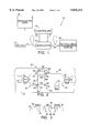
- FIG. 1 is a simplified schematic illustration of an optical system having a variable chirp modulator provided in accordance with the present invention.
- FIG. 2 is an enhanced schematic illustration of the variable chirp modulator of FIG. 1.
- FIG. 3 is a simplified schematic sectioned illustration of the modulator of FIG. 1 showing the relative location of several optical waveguides.
- FIG. 4 is a diagrammatic illustration of intensity of light output from the modulator of FIG. 2 at zero chirp.
- FIG. 5 is a diagrammatic illustration of phase of light output from the modulator of FIG. 2 at zero chirp.
- FIG. 6 is a diagrammatic illustration of intensity of light output from the modulator of FIG. 2 at a small value of chirp.
- FIG. 7 is a diagrammatic illustration of phase of light output from the device of FIG. 2 at a small value of chirp.
- FIG. 8 is a diagrammatic illustration of intensity of light output from the modulator of FIG. 2 at a first moderate value of chirp.
- FIG. 9 is a diagrammatic illustration of phase of light output from the modulator of FIG. 2 at a first moderate value of chirp.
- FIG. 10 is a diagrammatic illustration of intensity of light output from the modulator of FIG. 2 at a second moderate value of chirp.
- FIG. 11 is a diagrammatic illustration of phase of light output from the modulator of FIG. 2 at a second moderate value of chirp.
- FIG. 12 is a diagrammatic illustration of intensity of light output from the modulator of FIG. 2 at a large value of chirp.
- FIG. 13 is a diagrammatic illustration of phase of light output from the modulator of FIG. 2 at a large value of chirp.
- FIG. 14 is a diagrammatic illustration of intensity of light output from the modulator of FIG. 2 at a third moderate value of chirp.
- FIG. 15 is a diagrammatic illustration of phase of light output from the modulator of FIG. 2 at a third moderate value of chirp.
- FIG. 16 is a simplified schematic illustration of an alternative embodiment of the present invention in a cascaded modulator.
- FIG. 17 is a simplified schematic illustration of a second alternative embodiment of the present invention characterized by an extended frequency range over which chirp can be tuned.
- the present invention provides a variable chirp modulator which uses a single modulation signal to modulate an optical beam transiting the device.
- the single modulation voltage is applied in substantially equal amplitude to one or more electrodes in the preferred embodiment.
- the use of a single modulation signal eliminates problems associated with having two independent modulation voltages on the same modulator, such as interference effects on propagating optical beams, that result from microwave fields of different amplitudes.
- the complexity of the drive electronics is reduced substantially since only one modulation voltage must be applied instead of two time-synchronized modulation signals having unequal amplitude as with known devices.
- a chirp parameter for the modulator is adjusted by means of one or more DC voltages applied as a chirp control signal.
- the chirp control signal selects the magnitude of the light presented to the different legs of the modulator's interferometers.
- the chirp parameter for the modulator is adjustable over a range determined by individual chirp parameters for two Mach-Zehnder interferometers in the preferred embodiment.
- the reference legs can receive some level of modulation as compared to the "modulation" leg, although typically of lesser magnitude and/or opposite sign.
- FIGS. 1 and 2 there is shown a simplified schematic illustration of a fiber optic transmission system 10 having an optical modulator 12 that is an electro-optic device of a type provided in accordance with the present invention.
- An optical source 14 presents an optical beam to a fiber optic cable 16, which is connected to the input of the optical modulator.
- the optical beam is split into two signals by an input directional coupler 18 to a major interferometer 20 having within its branches two minor interferometers 22, 24.
- the interferometers are of a type known in the art, but are preferably of a Mach-Zehnder design.
- a radio frequency (RF) modulation signal is supplied by a signal generator associated with a controller 26 in dependence on modulation command signals from a modulation data source 28.
- the RF energy from the modulator is conducted within the modulator by modulation electrode 30.
- An output directional coupler 32 combines the two optical signals phase-shifted relative to one another into a single, amplitude modulated optical signal. Both the input and output directional couplers respectively split and combine light in accordance with received command signals presented on line 33.
- Fiber optic cable 34 is connected to the optical output of the modulator and delivers the modulated optical signal to the next device in the system 36.
- the optical wave travels down waveguides formed in the modulator. During transit, the electrical field of the RF signal modulates the optical wave.
- the distance in which the RF waves interact with or modulate the optical waves is called the interaction distance, and is determined primarily by the modulator design.
- the modulator includes a substrate 38 which is approximately 1000 ⁇ m thick.
- the length and width of substrate depend on the modulator design and should be sufficient to support the optical waveguides and the RF electrodes.
- the electro-optic effect displayed by the substrate relates to the change in the index of refraction of the substrate material as compared to the magnitude of the applied electric field.
- the effect is small and linear for substrates suitable for the present application. It is desirable to select a substrate material with a relatively high electro-optic coefficient. Accordingly, lithium niobate (LiNbO 3 ) was chosen, although other electro-optic materials, such as gallium arsenide (GaAs) may also be used.
- LiNbO 3 lithium niobate
- GaAs gallium arsenide
- the electro-optic effect in LiNbO 3 depends on the direction of the electric field relative to the orientation of the crystalline structure of the substrate along which the optical wave will propagate. There are two practical selections. The first is a crystallographic orientation where the optic axis is parallel to plane of the substrate and at right angles to the direction propagation of the optical wave, called an X-cut. The second is where the optic axis is normal to the of the substrate, referred to as a Z-cut. For the present application, Z-cut lithium niobate (LiNbO 3 ) is selected. Regardless, the applied electric field for maximum electro-optic interaction is in the direction of the optic axis.
- the preferred modulator includes first and second minor Mach-Zehnder interferometers formed by optical waveguides in respective legs 40, 42 of the major Mach-Zehnder interferometer.
- Each minor interferometer has optical waveguides 44, 46 and 48, 50. All of the optical waveguides are fabricated within the substrate, although alternative embodiments using ridge waveguides can be substituted.
- the waveguides are preferably created by diffusing titanium into the substrate.
- titanium is deposited as a strip on the surface of the crystal. Thereafter, the temperature of the substrate is raised so that the titanium diffuses into the substrate to form the channels that act as waveguides.
- the waveguides are approximately seven (7) microns wide and approximately three (3) microns deep.
- Fiber optic transmission media used in most optical communication links are dispersive, that is different wavelengths (or frequencies) of light travel at slightly different velocities. This effect causes optical pulses from a modulator to broaden as they travel down the fiber optic cable, causing greater difficulty at the receiver when reconstructing an electrical pulse from the received optical pulse.
- the power at the transmitter must be increased to overcome the degradation caused by dispersion. This increase in power required to maintain error free operation is referred to as the dispersion penalty of the communication link.
- the optical modulator produces a small amount of chirp of proper magnitude and sign, that is, the frequency of the light is shifted during the rising and falling edges of the optical pulse, the dispersion penalty can be significantly reduced, due to pulse compression that occurs.
- the optimal amount of modulator chirp depends on length of the fiber optic cable, therefore, it is desirable that the modulator chirp be variable, in order that one modulator can be used with any length of fiber optic cable.
- a variable chirp modulator provided in accordance with the present invention comprises several optical paths as embodied by the optical waveguides of the minor interferometers. These waveguides are fabricated in the proximity of the modulation electrode(s) which is driven by a single modulation source. By varying the optical amplitude or phase of the light in the different optical paths, the chirp of the modulator is varied. This preferably accomplished by directional coupler command signals provided to the modulator on line 51.
- the reference legs of the minor interferometers can receive some level of modulation as compared to the modulation legs, although typically of lesser magnitude and/or opposite sign.
- the four optical paths in the vicinity of the electrode of the preferred embodiment carry the modulation signal and provide adjustable chirp. Other numbers of optical paths are possible in alternative embodiments.
- the preferred design yields a net optical phase shift which is nearly linear with modulation voltage; a feature which makes the variable chirp modulator operate in a manner equivalent to fixed chirp, Mach-Zehnder modulators.
- the four optical waveguides of the minor Mach-Zehnder interferometers are all preferably formed with single mode optical waveguides. It is possible to use a combination of single or multi-mode waveguides or even discrete optics to perform the same task. However, the embodiment of FIG. 1 is preferable because of fabrication considerations.
- the minor interferometers employ Y-junctions 52, 54, 56, 58 to split the received optical beam as described hereinabove with respect to the major interferometer.
- Other power splitting/combining elements may be equivalently substituted.
- the input and output Y-junctions of the minor interferometers have power split ratios, respectively designated F2 and F3, of typically 50%.
- the total optical power flowing through the modulator is split between the minor interferometers by adjusting the power split ratios, F1 and F4, of the two electro-optically controlled, input and output directional couplers.
- F1 and F4 the power split ratios
- other types of adjustable power dividing/combining elements such as 1 ⁇ 2 couplers, can also be used instead of the more conventional 2 ⁇ 2 directional coupler switch of the embodiment of FIG. 2.
- bias electrode 60 after minor interferometer 24 which compensates for the phase shift through each coupler and any path length imbalance between the legs of the major interferometer.
- the bias electrode is set in order that light passing through the lower arm (in the Figure) of the major Mach-Zehnder interferometer experiences an extra ⁇ phase shift relative to the upper arm in order to cancel the ⁇ /2 phase shifts encountered when coupling across the directional couplers.
- the modulation signal voltage is applied to the modulation electrode which has on each side ground electrodes 62, 64 in order to form a Coplanar Waveguide (CPW) structure 67.
- the electric field generated by the CPW overlaps the optical waveguides of the minor interferometers, generating a phase shift proportional to voltage.
- the positions of the optical waveguides relative to each other and the electrodes are chosen in order that some of the phase shifts are different in each of the optical waveguides.
- the relative positions of the waveguides in the minor interferometers to the electrodes can be seen in the simplified sectional illustration of FIG. 3.
- the values V1, V2, V3, and V4 represent the phase shifts in each optical waveguide in a minor interferometer arm in units of ⁇ relative to the drive voltage on the modulation electrode.
- the waveguide positions are chosen in order that the voltage change from the "off” to "on” state (V.sub. ⁇ ) is the same for each minor interferometer, whereas the chirp parameter of the light at the output of each minor interferometer is different.
- the chirp parameter, ⁇ is defined by the following equation:
- I and ⁇ are the instantaneous intensity and phase, respectively, of the light output by a modulator.
- the chirp parameter of the entire modulator, ⁇ can be adjusted from -0.9 to 0.0 by adjusting the power split ratios F1 and F4.
- the power split ratio F1 is selected by the input directional coupler and power split ratio F4 by the output directional coupler.
- ⁇ can be adjusted from 0.0 to 0.9.
- Such a shift in the bias point corresponds to a bias point change on the intensity versus applied modulation signal transfer function to bias point with equivalent intensity magnitude but on a curve portion having opposite slope. For example in FIG. 4, points 71, 73 are shifted by ⁇ .
- chirp parameter measurement is typically done with a modulation signal of small amplitude.
- the modulator may be biased at other points when a large amplitude digital modulation signal is applied to the modulator. Note that the digital signal must be inverted when shifting the bias point to change sign of the chirp. For example, if a positive change in modulation voltage is required during the rising edge of the digital pulse for positive chirp, then a negative voltage change will be needed when the modulator is biased for negative chirp.
- the minor interferometers must be fabricated in such a way that their bias points are matched. That is, the minor interferometers are fully on or fully off at the same modulation voltage.
- the chirp parameter is selected to have a range so that the slope of the intensity versus applied modulation signal transfer function does not change sign; e.g. bias point 77 remains on a selected curve portion 79 of the transfer function peak 81, as seen in FIG. 6.
- FIGS. 4 through 13 show the calculated intensity and phase of the light output from the modulator for different values of power split ratios, F1 and F4.
- Curves 76, 78 of FIGS. 6 and 7 respectively correspond to the transfer function of intensity (P1k k ) and phase (Phase1 k ) vs. applied modulation signal (del k ).
- the response of the modulator for a second case of moderate chirp is seen in FIGS. 10, 11.
- the transfer functions of intensity (P1k k ) and phase (Phase1 k ) vs. applied modulation signal (del k ) are demonstrated by curves 84, 86.
- the transfer function of intensity (P1k k ) vs. applied modulation signal (del k ) is shown by curve 88 while that of phase (Phase1 k ) vs. applied modulation signal (del k ) is seen by curve 90.
- the transfer functions are intensity (P1k k ) vs. applied modulation signal (del k ) shown by curve 92 and phase (Phase1 k ) vs. applied modulation signal (del k ) illustrated by curve 94.
- V3 is altered from its previous value of 0.5 to 0.6 and V4 changes from -0.5 to -0.4.
- the chirp parameter, ⁇ changes from the previous example of value of -0.4 to -0.5.
- the range of chirp parameter is adjustable over a smaller range, from -0.2 to -0.9 instead of 0.0 to -0.9, the range of the examples shown with respect to FIGS. 4-13.
- FIG. 16 schematically shows an alternative embodiment of the present invention characterized by a cascaded interferometer design.
- a cascaded modulator 96 is similar to the embodiment of FIG. 2 but separates the modulation of the optical signal from chirp compensation without the use of a major interferometer.
- An input optical beam 97 is presented to a first interferometer 98 and split into two equal signals by a Y-junction 100.
- An RF modulation signal from an external signal generator is presented to a central modulation electrode 102.
- External ground electrodes 104, 106 are fabricated adjacent to optical waveguides 108, 110. The energy from the modulation signal is communicated with both of these optical waveguides.
- a second Y junction 112 recombines the modulated signals before presentation to a first directional coupler 114.
- the first directional coupler presents optical power of a selected magnitude to legs 116, 118 of a second interferometer 120.
- the interferometers are of a type known in the art, but are preferably of a Mach-Zehnder design.
- the optical waveguides which comprise legs 116, 118 encompass a modulation electrode 122 which receives the same modulation signal as does modulation electrode 102.
- the second interferometer is bounded by ground electrodes 104, 106.
- An output directional coupler 124 combines the two optical signals phase-shifted relative to one another into a single, amplitude modulated optical signal for presentation to a fiber optic cable 126.
- the modulator chirp parameter, ⁇ is selected as in the preferred embodiment by varying the power split ratio between the input and output directional couplers.
- FIG. 17 there is schematically shown a second alternative embodiment of the present invention as modulator 128.
- the modulator includes a subassembly 130 encompassed within the larger dashed box which is substantially equivalent to the single source variable chirp modulator described hereinabove.
- the subassembly has two interferometers 142, 144 as well as input and output directional couplers 146, 148. Interferometers 142, 144 each have reference and modulation legs indicated by waveguides 162, 164 and 166, 168.
- the modulator 128 also includes a supplemental interferometer 132 of the type described hereinabove and contained within the smaller dashed box and which has reference and modulation legs indicated by waveguides 170, 172.
- a supplemental interferometer 132 of the type described hereinabove and contained within the smaller dashed box and which has reference and modulation legs indicated by waveguides 170, 172.
- Light from modulator input directional coupler 134 is presented to both the subassembly 130 and interferometer 132 in accordance with a desired power split ratio F1 b.
- modulator output directional coupler 136 which receives light from the subassembly 130 and interferometer 132 and combines the same in accordance with a power split ratio F4b.
- the modulator 128 also includes bias electrodes, 138 and 140 which receive bias control signals to compensate for the phase shift through each coupler as well as any path length imbalance between legs of the interferometers, as described hereinabove.
- the values V1-V6 represent the respective phase shifts in each optical waveguide in an interferometer arm in units of ⁇ relative to the drive voltage on the modulation electrode.
- the waveguide positions are chosen in order that the voltage change from the "off” to "on” state (V.sub. ⁇ ) is the same for each minor interferometer, whereas the chirp parameter of the light at the output of each minor interferometer is different.
- the split ratios F1a and F4a are set to 0.0 when F1b and F4b are less than 1.0. That is, the subassembly is set to have a chirp parameter of 0.0 when optical power is diverted to the interferometer 132 in order to maintain linearity of the optical phase vs. modulator signal transfer function.
- V mod the modulation signal from source 150 is applied to two electrodes 152, 154 instead of one in the embodiment of FIG. 2. However, the voltages on those electrodes are equal in amplitude, in order to prevent interference effects. Also shown in the Figure are ground electrodes 156, 158 and 160.
Abstract
Description
α=(dφ/dt)/(dI/dt)/2I
Claims (20)
Priority Applications (7)
| Application Number | Priority Date | Filing Date | Title |
|---|---|---|---|
| US08/731,760 US5835212A (en) | 1996-10-18 | 1996-10-18 | Variable chirp optical modulator using single modulation source |
| PCT/US1997/018198 WO1998017967A1 (en) | 1996-10-18 | 1997-10-17 | Variable chirp optical modulator using single modulation source |
| AU50797/98A AU5079798A (en) | 1996-10-18 | 1997-10-17 | Variable chirp optical modulator using single modulation source |
| JP51942098A JP3433753B2 (en) | 1996-10-18 | 1997-10-17 | Tunable chirped light modulator using a single modulation source |
| DE69722443T DE69722443T2 (en) | 1996-10-18 | 1997-10-17 | Variable optical chirp modulator with a single modulation source |
| CA002272376A CA2272376A1 (en) | 1996-10-18 | 1997-10-17 | Variable chirp optical modulator using single modulation source |
| EP97913667A EP0950167B1 (en) | 1996-10-18 | 1997-10-17 | Variable chirp optical modulator using single modulation source |
Applications Claiming Priority (1)
| Application Number | Priority Date | Filing Date | Title |
|---|---|---|---|
| US08/731,760 US5835212A (en) | 1996-10-18 | 1996-10-18 | Variable chirp optical modulator using single modulation source |
Publications (1)
| Publication Number | Publication Date |
|---|---|
| US5835212A true US5835212A (en) | 1998-11-10 |
Family
ID=24940855
Family Applications (1)
| Application Number | Title | Priority Date | Filing Date |
|---|---|---|---|
| US08/731,760 Expired - Fee Related US5835212A (en) | 1996-10-18 | 1996-10-18 | Variable chirp optical modulator using single modulation source |
Country Status (6)
| Country | Link |
|---|---|
| US (1) | US5835212A (en) |
| EP (1) | EP0950167B1 (en) |
| JP (1) | JP3433753B2 (en) |
| AU (1) | AU5079798A (en) |
| DE (1) | DE69722443T2 (en) |
| WO (1) | WO1998017967A1 (en) |
Cited By (39)
| Publication number | Priority date | Publication date | Assignee | Title |
|---|---|---|---|---|
| US5973816A (en) * | 1997-08-28 | 1999-10-26 | Fujitsu Limited | Method and apparatus of driving an optical modulator to measure, and compensation for dispersion in an optical transmission line |
| US6118397A (en) * | 1998-06-17 | 2000-09-12 | Trw Inc. | Fully optical analog to digital converters with complementary outputs |
| US6198855B1 (en) | 1996-07-19 | 2001-03-06 | Jds Uniphase Corporation | Velocity-matched, traveling-wave electro-optical devices using non-conductive and conductive polymer buffer layers |
| US6341031B1 (en) | 1999-05-25 | 2002-01-22 | Jds Uniphase Corporation | Optical pulse generation using a high order function waveguide interferometer |
| US6369897B1 (en) | 2000-01-28 | 2002-04-09 | The Boeing Company | Fiber optic receiving antenna |
| US6407846B1 (en) | 2001-03-16 | 2002-06-18 | All Optical Networks, Inc. | Photonic wavelength shifting method |
| US6445841B1 (en) | 1999-05-28 | 2002-09-03 | Omm, Inc. | Optomechanical matrix switches including collimator arrays |
| US6445840B1 (en) | 1999-05-28 | 2002-09-03 | Omm, Inc. | Micromachined optical switching devices |
| US6449406B1 (en) | 1999-05-28 | 2002-09-10 | Omm, Inc. | Micromachined optomechanical switching devices |
| US6453083B1 (en) | 1999-05-28 | 2002-09-17 | Anis Husain | Micromachined optomechanical switching cell with parallel plate actuator and on-chip power monitoring |
| US20020131125A1 (en) * | 2001-03-16 | 2002-09-19 | Myers Michael H. | Replicated-spectrum photonic transceiving |
| US6490044B1 (en) * | 1997-05-30 | 2002-12-03 | Jds Uniphase Corporation | Optimized interferometrically modulated array source |
| US6498870B1 (en) | 1998-04-20 | 2002-12-24 | Omm, Inc. | Micromachined optomechanical switches |
| US6532315B1 (en) * | 2000-10-06 | 2003-03-11 | Donald J. Lenkszus | Variable chirp optical modulator having different length electrodes |
| US6535653B1 (en) * | 2000-10-06 | 2003-03-18 | Donald J. Lenkszus | Variable chirp optical modulator |
| US20030081277A1 (en) * | 2001-11-01 | 2003-05-01 | Sacha Corbeil | Adaptive method for chirping an optical data signal |
| US20040008395A1 (en) * | 2000-11-22 | 2004-01-15 | Jds Uniphase Corporation | Cascaded RZ and NRZ laser modulators having RZ/NRZ phase alignment bias control |
| US6714695B2 (en) | 2001-09-17 | 2004-03-30 | Dorsal Networks, Inc. | Optical transmission system employing auto-synchronized chirped return-to-zero transmitter |
| WO2004030242A1 (en) * | 2002-09-26 | 2004-04-08 | Bookham Technology Plc | Electro-optic modulator witih continuously adjustable chirp |
| US20040096143A1 (en) * | 2001-09-26 | 2004-05-20 | Celight, Inc. | Coherent optical detector and coherent communication system and method |
| US6744909B1 (en) | 1999-08-19 | 2004-06-01 | Physical Optics Corporation | Authentication system and method |
| US20040240765A1 (en) * | 2003-05-30 | 2004-12-02 | Jds Uniphase Corporation | Optical digital external modulator |
| US20050111853A1 (en) * | 2003-10-10 | 2005-05-26 | Tetsuya Kawanishi | Optical frequency shift keying modulator |
| US20050213862A1 (en) * | 2004-03-16 | 2005-09-29 | Tetsuya Kawanishi | Bias adjustment method for optical SSB modulator or optical FSK modulator |
| US7212326B2 (en) | 2003-05-30 | 2007-05-01 | Jds Uniphase Corporation | Optical external modulator |
| US20070280701A1 (en) * | 2004-05-25 | 2007-12-06 | Azea Networks Limited | Method and Apparatus for Producing High Extinction Ratio Data Modulation Formats |
| US20080008412A1 (en) * | 2005-03-18 | 2008-01-10 | Fujitsu Limited | Optical device |
| US20080144989A1 (en) * | 2004-12-22 | 2008-06-19 | Advantest Corporation | Optical switch and optical test apparatus |
| US7499603B1 (en) * | 2006-01-19 | 2009-03-03 | Lockheed Martin Corporation | Range extended electrooptic modulator |
| US20090225333A1 (en) * | 2008-03-05 | 2009-09-10 | Clark Alexander Bendall | System aspects for a probe system that utilizes structured-light |
| US20090231685A1 (en) * | 2008-03-11 | 2009-09-17 | Jyehong Chen | Optical amplifier for tuning transmission time of optical signal |
| US20100060972A1 (en) * | 2008-09-08 | 2010-03-11 | Daniel Kucharski | Method and circuit for encoding multi-level pulse amplitude modulated signals using integrated optoelectronic devices |
| US20110158576A1 (en) * | 2009-12-30 | 2011-06-30 | Jds Uniphase Corporation | Optical waveguide modulator |
| US20110221627A1 (en) * | 2008-09-18 | 2011-09-15 | Selex Sistemi Integrati S.P.A. | Switchable delays optical fibre transponder with optical generation of doppler shift |
| US20160282699A1 (en) * | 2013-03-20 | 2016-09-29 | Xieon Networks S.À.R.L. | Optical iq modulator control |
| US20170356987A1 (en) * | 2014-04-09 | 2017-12-14 | Digital Signal Corporation | System and Method for Using Combining Couplers with Asymmetric Split Ratios in a Lidar System |
| US10303036B2 (en) * | 2016-09-20 | 2019-05-28 | Fujitsu Optical Components Limited | Optical modulator |
| US10509243B2 (en) | 2017-03-15 | 2019-12-17 | Elenion Technologies, Llc | Bias control of optical modulators |
| US10742324B1 (en) | 2019-05-21 | 2020-08-11 | Elenion Technologies, Llc | Bias control of optical modulators |
Families Citing this family (5)
| Publication number | Priority date | Publication date | Assignee | Title |
|---|---|---|---|---|
| JP5303951B2 (en) * | 2008-02-12 | 2013-10-02 | 日本電気株式会社 | Optical modulator and optical modulation method |
| EP2323287A1 (en) * | 2009-11-12 | 2011-05-18 | Intune Networks Limited | Modulator control system and method in an optical network |
| JP5304938B2 (en) * | 2012-10-01 | 2013-10-02 | 日本電気株式会社 | Optical modulator and optical modulation method |
| US9599504B2 (en) * | 2013-07-30 | 2017-03-21 | Raytheon Company | Fiber optic vibration detection |
| CN109661612B (en) | 2016-07-22 | 2023-04-04 | 光子系统股份有限公司 | Inherently broadband linearized electro-optic modulator with customizable performance |
Citations (1)
| Publication number | Priority date | Publication date | Assignee | Title |
|---|---|---|---|---|
| US5101450A (en) * | 1991-01-23 | 1992-03-31 | Gte Laboratories Incorporated | Quadrature optical phase modulators for lightwave systems |
Family Cites Families (3)
| Publication number | Priority date | Publication date | Assignee | Title |
|---|---|---|---|---|
| JPS59107324A (en) * | 1982-12-13 | 1984-06-21 | Fujitsu Ltd | Optical modulator |
| JPS6368825A (en) * | 1986-09-10 | 1988-03-28 | Hitachi Ltd | Optical modulating element array |
| US5168534A (en) * | 1991-12-09 | 1992-12-01 | United Technologies Corporation | Cascaded optic modulator arrangement |
-
1996
- 1996-10-18 US US08/731,760 patent/US5835212A/en not_active Expired - Fee Related
-
1997
- 1997-10-17 WO PCT/US1997/018198 patent/WO1998017967A1/en active IP Right Grant
- 1997-10-17 EP EP97913667A patent/EP0950167B1/en not_active Expired - Lifetime
- 1997-10-17 DE DE69722443T patent/DE69722443T2/en not_active Expired - Fee Related
- 1997-10-17 JP JP51942098A patent/JP3433753B2/en not_active Expired - Fee Related
- 1997-10-17 AU AU50797/98A patent/AU5079798A/en not_active Abandoned
Patent Citations (1)
| Publication number | Priority date | Publication date | Assignee | Title |
|---|---|---|---|---|
| US5101450A (en) * | 1991-01-23 | 1992-03-31 | Gte Laboratories Incorporated | Quadrature optical phase modulators for lightwave systems |
Non-Patent Citations (2)
| Title |
|---|
| "Integrated Optical SSB Modular/Frequency Shifter" by Masayuki Izutsu, Shinsuke Shikama, and Tadasi Sueta; IEEE Journal of Quantum Electronics, vol. QE-17, No. 11, Nov. 1981. |
| Integrated Optical SSB Modular/Frequency Shifter by Masayuki Izutsu, Shinsuke Shikama, and Tadasi Sueta; IEEE Journal of Quantum Electronics, vol. QE 17, No. 11, Nov. 1981. * |
Cited By (59)
| Publication number | Priority date | Publication date | Assignee | Title |
|---|---|---|---|---|
| US6198855B1 (en) | 1996-07-19 | 2001-03-06 | Jds Uniphase Corporation | Velocity-matched, traveling-wave electro-optical devices using non-conductive and conductive polymer buffer layers |
| US6490044B1 (en) * | 1997-05-30 | 2002-12-03 | Jds Uniphase Corporation | Optimized interferometrically modulated array source |
| US5973816A (en) * | 1997-08-28 | 1999-10-26 | Fujitsu Limited | Method and apparatus of driving an optical modulator to measure, and compensation for dispersion in an optical transmission line |
| US5982530A (en) * | 1997-08-28 | 1999-11-09 | Fujitsu Limited | Apparatus for driving an optical modulator to measure, and compensate for, dispersion in an optical transmission line |
| US6262828B1 (en) | 1997-08-28 | 2001-07-17 | Fujitsu Limited | Method and apparatus of driving an optical modulator to measure, and compensate for, dispersion in an optical transmission line |
| US6526198B1 (en) | 1998-04-20 | 2003-02-25 | Omm, Inc. | Micromachined optomechanical switches |
| US6498870B1 (en) | 1998-04-20 | 2002-12-24 | Omm, Inc. | Micromachined optomechanical switches |
| US6404365B1 (en) * | 1998-06-17 | 2002-06-11 | Trw Inc. | Fully optical analog to digital converters with complementary outputs |
| US6118397A (en) * | 1998-06-17 | 2000-09-12 | Trw Inc. | Fully optical analog to digital converters with complementary outputs |
| US6341031B1 (en) | 1999-05-25 | 2002-01-22 | Jds Uniphase Corporation | Optical pulse generation using a high order function waveguide interferometer |
| US6445841B1 (en) | 1999-05-28 | 2002-09-03 | Omm, Inc. | Optomechanical matrix switches including collimator arrays |
| US6445840B1 (en) | 1999-05-28 | 2002-09-03 | Omm, Inc. | Micromachined optical switching devices |
| US6449406B1 (en) | 1999-05-28 | 2002-09-10 | Omm, Inc. | Micromachined optomechanical switching devices |
| US6453083B1 (en) | 1999-05-28 | 2002-09-17 | Anis Husain | Micromachined optomechanical switching cell with parallel plate actuator and on-chip power monitoring |
| US7317814B2 (en) | 1999-08-19 | 2008-01-08 | Physical Optics Corporation | Authentication system and method |
| US6744909B1 (en) | 1999-08-19 | 2004-06-01 | Physical Optics Corporation | Authentication system and method |
| US6369897B1 (en) | 2000-01-28 | 2002-04-09 | The Boeing Company | Fiber optic receiving antenna |
| US6532315B1 (en) * | 2000-10-06 | 2003-03-11 | Donald J. Lenkszus | Variable chirp optical modulator having different length electrodes |
| US6535653B1 (en) * | 2000-10-06 | 2003-03-18 | Donald J. Lenkszus | Variable chirp optical modulator |
| US6917455B2 (en) | 2000-11-22 | 2005-07-12 | Jds Uniphase Corporation | Cascaded RZ and NRZ laser modulators having RZ/NRZ phase alignment bias control |
| US20040008395A1 (en) * | 2000-11-22 | 2004-01-15 | Jds Uniphase Corporation | Cascaded RZ and NRZ laser modulators having RZ/NRZ phase alignment bias control |
| US20020131125A1 (en) * | 2001-03-16 | 2002-09-19 | Myers Michael H. | Replicated-spectrum photonic transceiving |
| US6407846B1 (en) | 2001-03-16 | 2002-06-18 | All Optical Networks, Inc. | Photonic wavelength shifting method |
| US6714695B2 (en) | 2001-09-17 | 2004-03-30 | Dorsal Networks, Inc. | Optical transmission system employing auto-synchronized chirped return-to-zero transmitter |
| US20040096143A1 (en) * | 2001-09-26 | 2004-05-20 | Celight, Inc. | Coherent optical detector and coherent communication system and method |
| US7327913B2 (en) * | 2001-09-26 | 2008-02-05 | Celight, Inc. | Coherent optical detector and coherent communication system and method |
| US20030081277A1 (en) * | 2001-11-01 | 2003-05-01 | Sacha Corbeil | Adaptive method for chirping an optical data signal |
| US6999678B2 (en) | 2001-11-01 | 2006-02-14 | Pts Corporation | Adaptive method for chirping an optical data signal |
| WO2004030242A1 (en) * | 2002-09-26 | 2004-04-08 | Bookham Technology Plc | Electro-optic modulator witih continuously adjustable chirp |
| US6961166B2 (en) | 2003-05-30 | 2005-11-01 | Jds Uniphase Corporation | Optical digital external modulator |
| US20040240765A1 (en) * | 2003-05-30 | 2004-12-02 | Jds Uniphase Corporation | Optical digital external modulator |
| US7212326B2 (en) | 2003-05-30 | 2007-05-01 | Jds Uniphase Corporation | Optical external modulator |
| US20050111853A1 (en) * | 2003-10-10 | 2005-05-26 | Tetsuya Kawanishi | Optical frequency shift keying modulator |
| US7526209B2 (en) * | 2003-10-10 | 2009-04-28 | National Institute Of Information And Communications Technology | Optical frequency shift keying modulator |
| US7245787B2 (en) * | 2004-03-16 | 2007-07-17 | National Institute Of Information And Communications Technology, Incorporated Administrative Agency | Bias adjustment method for optical SSB modulator or optical FSK modulator |
| US20050213862A1 (en) * | 2004-03-16 | 2005-09-29 | Tetsuya Kawanishi | Bias adjustment method for optical SSB modulator or optical FSK modulator |
| US20070280701A1 (en) * | 2004-05-25 | 2007-12-06 | Azea Networks Limited | Method and Apparatus for Producing High Extinction Ratio Data Modulation Formats |
| US20080144989A1 (en) * | 2004-12-22 | 2008-06-19 | Advantest Corporation | Optical switch and optical test apparatus |
| US7519241B2 (en) * | 2005-03-18 | 2009-04-14 | Fujitsu Limited | Optical device |
| US20080008412A1 (en) * | 2005-03-18 | 2008-01-10 | Fujitsu Limited | Optical device |
| US7499603B1 (en) * | 2006-01-19 | 2009-03-03 | Lockheed Martin Corporation | Range extended electrooptic modulator |
| US20090225333A1 (en) * | 2008-03-05 | 2009-09-10 | Clark Alexander Bendall | System aspects for a probe system that utilizes structured-light |
| US20090231685A1 (en) * | 2008-03-11 | 2009-09-17 | Jyehong Chen | Optical amplifier for tuning transmission time of optical signal |
| US20170126325A1 (en) * | 2008-09-08 | 2017-05-04 | Luxtera, Inc. | Method and system for encoding multi-level pulse amplitude modulated signals using integrated optoelectronic devices |
| US9548811B2 (en) | 2008-09-08 | 2017-01-17 | Luxtera, Inc. | Method and system for encoding multi-level pulse amplitude modulated signals using integrated optoelectronic devices |
| US11212007B2 (en) | 2008-09-08 | 2021-12-28 | Luxtera Llc | Method and system for encoding multi-level pulse amplitude modulated signals using integrated optoelectronic devices |
| US8238014B2 (en) * | 2008-09-08 | 2012-08-07 | Luxtera Inc. | Method and circuit for encoding multi-level pulse amplitude modulated signals using integrated optoelectronic devices |
| US10305597B2 (en) * | 2008-09-08 | 2019-05-28 | Luxtera, Inc. | Method and system for encoding multi-level pulse amplitude modulated signals using integrated optoelectronic devices |
| US20100060972A1 (en) * | 2008-09-08 | 2010-03-11 | Daniel Kucharski | Method and circuit for encoding multi-level pulse amplitude modulated signals using integrated optoelectronic devices |
| US8466831B2 (en) * | 2008-09-18 | 2013-06-18 | Selex Sistemi Integrati S.P.A. | Switchable delays optical fibre transponder with optical generation of doppler shift |
| US20110221627A1 (en) * | 2008-09-18 | 2011-09-15 | Selex Sistemi Integrati S.P.A. | Switchable delays optical fibre transponder with optical generation of doppler shift |
| US8849071B2 (en) * | 2009-12-30 | 2014-09-30 | Jds Uniphase Corporation | Optical waveguide modulator |
| US20110158576A1 (en) * | 2009-12-30 | 2011-06-30 | Jds Uniphase Corporation | Optical waveguide modulator |
| US20160282699A1 (en) * | 2013-03-20 | 2016-09-29 | Xieon Networks S.À.R.L. | Optical iq modulator control |
| US9823540B2 (en) * | 2013-03-20 | 2017-11-21 | Xieon Networks S.A.R.L. | Optical IQ modulator control |
| US20170356987A1 (en) * | 2014-04-09 | 2017-12-14 | Digital Signal Corporation | System and Method for Using Combining Couplers with Asymmetric Split Ratios in a Lidar System |
| US10303036B2 (en) * | 2016-09-20 | 2019-05-28 | Fujitsu Optical Components Limited | Optical modulator |
| US10509243B2 (en) | 2017-03-15 | 2019-12-17 | Elenion Technologies, Llc | Bias control of optical modulators |
| US10742324B1 (en) | 2019-05-21 | 2020-08-11 | Elenion Technologies, Llc | Bias control of optical modulators |
Also Published As
| Publication number | Publication date |
|---|---|
| EP0950167A4 (en) | 2001-02-07 |
| EP0950167A1 (en) | 1999-10-20 |
| EP0950167B1 (en) | 2003-05-28 |
| WO1998017967A1 (en) | 1998-04-30 |
| DE69722443D1 (en) | 2003-07-03 |
| DE69722443T2 (en) | 2004-04-08 |
| JP3433753B2 (en) | 2003-08-04 |
| AU5079798A (en) | 1998-05-15 |
| JP2001503157A (en) | 2001-03-06 |
Similar Documents
| Publication | Publication Date | Title |
|---|---|---|
| US5835212A (en) | Variable chirp optical modulator using single modulation source | |
| US5991471A (en) | Configurable chirp mach-zehnder optical modulator | |
| US5926297A (en) | Optical modulating device and optical modulating method | |
| US6583917B2 (en) | Optical intensity modulation device and method | |
| US8149492B2 (en) | Optical modulator | |
| US6501867B2 (en) | Chirp compensated Mach-Zehnder electro-optic modulator | |
| US5303079A (en) | Tunable chirp, lightwave modulator for dispersion compensation | |
| US6392751B1 (en) | Optimized interferometrically modulated array source | |
| US6650458B1 (en) | Electro-optic modulator with continuously adjustable chirp | |
| US5408544A (en) | Optical modulator for producing a controllable chirp | |
| US5420868A (en) | Suppression of brillouin scattering in lightwave transmission system | |
| US5109441A (en) | Fiber optic external modulator | |
| KR101160435B1 (en) | Resonator-assisted control of radio-frequency response in an optical modulator | |
| US20060120655A1 (en) | Optical modulator with pre-determined frequency chirp | |
| US6341031B1 (en) | Optical pulse generation using a high order function waveguide interferometer | |
| US5652807A (en) | Semiconductor optical modulator | |
| JP3820009B2 (en) | Optical modulator and optical modulation method | |
| EP1424591A1 (en) | Electro-optical modulator and method of modulating optical signals | |
| JP2658387B2 (en) | Optical modulator, driving method thereof, and optical modulator driving device | |
| CA2366136C (en) | Optical intensity modulation device and method | |
| JPH0764031A (en) | Optical modulator | |
| US6947617B2 (en) | Polarized wave scrambler and optical signal transmission apparatus | |
| CA2272376A1 (en) | Variable chirp optical modulator using single modulation source | |
| JPH02239223A (en) | Optical modulator | |
| GB2361369A (en) | Optical modulator with time division multiplexing and chirping |
Legal Events
| Date | Code | Title | Description |
|---|---|---|---|
| AS | Assignment |
Owner name: UNIPHASE CORPORATION, CALIFORNIA Free format text: ASSIGNMENT OF ASSIGNORS INTEREST;ASSIGNORS:KISSA, KARL;LIN, JACK;REEL/FRAME:008234/0263 Effective date: 19961017 |
|
| AS | Assignment |
Owner name: UNIPHASE TELECOMMUNICATIONS PRODUCTS, INC., CONNEC Free format text: ASSIGNMENT OF ASSIGNORS INTEREST;ASSIGNOR:UNIPHASE CORPORATION;REEL/FRAME:009584/0688 Effective date: 19980622 |
|
| FPAY | Fee payment |
Year of fee payment: 4 |
|
| REMI | Maintenance fee reminder mailed | ||
| AS | Assignment |
Owner name: JDS UNIPHASE CORPORATION, CALIFORNIA Free format text: ASSIGNMENT OF ASSIGNORS INTEREST;ASSIGNOR:UNIPHASE TELECOMMUNICATIONS PRODUCTS, INC.;REEL/FRAME:013295/0189 Effective date: 20020815 |
|
| FPAY | Fee payment |
Year of fee payment: 8 |
|
| REMI | Maintenance fee reminder mailed | ||
| LAPS | Lapse for failure to pay maintenance fees | ||
| LAPS | Lapse for failure to pay maintenance fees |
Free format text: PATENT EXPIRED FOR FAILURE TO PAY MAINTENANCE FEES (ORIGINAL EVENT CODE: EXP.); ENTITY STATUS OF PATENT OWNER: LARGE ENTITY |
|
| STCH | Information on status: patent discontinuation |
Free format text: PATENT EXPIRED DUE TO NONPAYMENT OF MAINTENANCE FEES UNDER 37 CFR 1.362 |
|
| FP | Lapsed due to failure to pay maintenance fee |
Effective date: 20101110 |
|
| FEPP | Fee payment procedure |
Free format text: PAYOR NUMBER ASSIGNED (ORIGINAL EVENT CODE: ASPN); ENTITY STATUS OF PATENT OWNER: LARGE ENTITY |