US5856753A - Output circuit for 3V/5V clock chip duty cycle adjustments - Google Patents
Output circuit for 3V/5V clock chip duty cycle adjustments Download PDFInfo
- Publication number
- US5856753A US5856753A US08/624,925 US62492596A US5856753A US 5856753 A US5856753 A US 5856753A US 62492596 A US62492596 A US 62492596A US 5856753 A US5856753 A US 5856753A
- Authority
- US
- United States
- Prior art keywords
- circuit
- duty cycle
- timing signal
- supply voltage
- signal
- Prior art date
- Legal status (The legal status is an assumption and is not a legal conclusion. Google has not performed a legal analysis and makes no representation as to the accuracy of the status listed.)
- Expired - Lifetime
Links
Images

Classifications
-
- H—ELECTRICITY
- H03—ELECTRONIC CIRCUITRY
- H03K—PULSE TECHNIQUE
- H03K5/00—Manipulating of pulses not covered by one of the other main groups of this subclass
- H03K5/01—Shaping pulses
- H03K5/02—Shaping pulses by amplifying
- H03K5/023—Shaping pulses by amplifying using field effect transistors
Definitions
- the present invention relates to circuits for maintaining a constant duty cycle in a timing chip and, more particularly, to a circuit for maintaining a constant duty cycle in a timing chip that operates at either 3 volts or 5 volts without the need to preprogram the circuit to work at a specific supply voltage.
- a clock duty cycle is measured at 1.4 volts (for a TTL input).
- a desired duty cycle performance may be, for example, about 50% across process, temperature and voltage ranges for output frequencies up to 140 MHz (5V) or 122 MHz (3V).
- a desired slew rate may be, for example, between 1 V/ns-2 V/ns.
- Clock jitter should be relatively low. For example, less than 250 ps jitter is acceptable. Traditional clock drivers may not meet these specifications which may be required for certain modern IC applications.
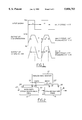
- FIG. 1 illustrates a comparison between a pad operating at 5 volts and an otherwise identical pad operating at 3 volts. When the pad above is operating at 3 volts, the rising edge becomes much slower and the measuring point is closer to Vcc. As a result, a very low duty cycle is realized.
- One approach uses a programmable element to control a portion of a pull down transistor. This allows the adjustment of the effective output threshold for the desired operating voltage.
- a major disadvantage of this approach is that the operating voltage must be known while building the programming vectors necessary for the manufacturing of the IC. After the internal fuses of the IC are programmed, the IC typically works only at the specified operating voltage. This tends to increase the complexity of manufacturing as well as the time necessary to generate samples. For example, a manufacturer generally must stock both 3 volt and 5 volt versions of the same part to meet demand.
- a second approach may realize a 50% duty cycle at both 3 and 5 volt operating voltages by using an on-chip voltage detector in place of the programmable element.
- the effect on signal control in the output pull down transistor is the same as in the approach discussed above.
- the second approach provides the advantage of being able to work with either voltage range (e.g., 3.0-3.6V or 4.5-5.5V).
- One disadvantage of the second approach is that the part tends to operate erratically in the voltage range between 3.6 and 4.5V. This erratic behavior is often directly translated into output jitter. Additionally, it is often difficult to reliably detect a voltage between 3.6 and 4.5 volts under noisy operating conditions.
- a third approach may realize a 50% duty cycle at both 3 and 5 volt operating voltages by increasing the edge rates of the output signal. This improves the duty cycle by reducing the time difference between the output threshold voltages.
- the third approach may be undesirable because a faster edge rate increases the on-chip noise problems and the EMI radiation.
- the required edge rates for the desired duty cycle performance are three to five times faster than current produce able values. Increased on-chip noise resulting from increasing the edge rates directly increases the part jitter.
- a fourth approach realizes a 50% duty cycle at both 3 volt and 5 volt operating voltages by changing the specifications to work around the duty cycle problem. For example, the duty cycle specification may only be met at a lower frequency. This may also be undesirable since conditions under which parts meet duty cycle and other specifications are becoming stricter with time.
- the present invention provides an analog biased pre-driver and pad as well as a duty cycle adjustment cell prior to the pre-driver and pad.
- the pre-driver and pad may operate in either a 3 volt mode, a 5 volt mode or any voltage in between, depending only on the power supply voltage present. No production configuration or post-production configuration is required.
- the present invention utilizes a special bias circuit to reduce the Vcc, temperature and other processing variations.
- a duty cycle cell produces a range of duty cycles when the circuit is operating between a 3 volt and 5 volt range. Based on different supply voltages, the duty cycle is adjusted before the pre-driver and driver.
- the pre-driver and driver can output a 50% duty cycle for a TTL input regardless the supply voltage Vcc.
- the objects, features and advantages of the present invention include providing a clock chip that operates at a constant duty cycle and which does not need reconfiguration.
- the clock chip works for both 3 volt and 5 volt designs interchangeably without reconfiguration and provides continuous operation over the entire voltage operating range. Consequently, the clock circuit may reduce chip noise and clock jitter at the output, shorten the design cycle, assure a low jitter under all conditions, and achieves a high Power Supply Rejection Ratio (PSRR).
- PSRR Power Supply Rejection Ratio
- FIG. 1 is a timing diagram illustrating the different duty cycles when a identical clock chip operates at 3 volts and 5 volts;
- FIG. 2 is a block diagram of a preferred embodiment of the present invention.
- FIG. 3 is a circuit diagram illustrating a duty cycle adjustment cell
- FIG. 4 is a circuit diagram illustrating the pre-driver and pad.
- the circuit 10 generally comprises an analog bias circuit 12, a duty cycle adjustment cell 14 and a pre-driver and optional pad circuit 16.
- the analog bias circuit 12 has an output 18 that provides a biasN signal to the duty cycle adjustment cell 14 and to the pre-driver and pad circuit 16.
- the analog bias circuit 12 also has an output 20 that provides a biasP signal to the duty cycle adjustment cell 14 and to the pre-driver and pad circuit 16.
- the duty cycle adjustment cell 14 has an input 22 that receives a 50% duty cycle signal (measured at Vcc/2), an input 24 that receives the biasN signal and an input 26 that receives the biasP signal.
- the duty cycle adjustment cell 14 presents an output 28 that is received at an input 30 of the pre-driver and pad circuit 16.
- the pre-driver and pad circuit 16 also has an input 32 that receives the biasN signal and an input 34 that receives the biasP signal.
- the pre-driver and pad circuit 16 presents an output 36 that produces a 50% duty cycle signal measured at 1.4 volts.
- the supply voltage to the circuit may be, in one example, at least 2.7v and may, in one example, range from about 3 to about 5v, and in another example, may range from 2.7v to about 6v.
- a "50% duty cycle signal” refers to a desired duty cycle signal which in its most preferred embodiment, is about 50%. However, it may be any desired level, for example, from 30% to 70%, and more preferably, from about 40% to 60%.
- the duty cycle adjustment cell 14 may provide an adjustment to the signal received at the input 22. At 5v operation, the duty cycle adjustment cell 14 outputs a much lower duty cycle signal at the output 28 because of a very fast falling edge. After the pre-driver and pad 16, the output duty cycle signal will be larger (measure at 1.4v) than the duty cycle at the input since the internal duty cycle is measured at Vcc/2. The duty cycle at the output 28 may be lower so the duty cycle at the output 36 can be 50%.
- the analog bias circuit 12 provides the output 18 and the output 20 that may provide adjustments for temperature and other processing parameter variations in the operation of the circuit 10. Any type of analog bias circuit 12 that produces process temperature and Vcc self-compensation may be used.
- the duty cycle adjustment cell 14 generally comprises a transistor 38, a transistor 40, a transistor 42, a transistor 44, a transistor 46, a transistor 48, a resistor 50 and a resistor 52.
- the resistors 50 and 52 in one example, have a 2:1 ratio.
- the transistors 38, 40, 42 and 44 form an input section 45.
- a supply voltage Vcc is presented to the sources of the transistors 38 and 48.
- the drains of the transistors 44 and 46 are connected to ground.
- An inverted gate of the transistor 38 receives the biasP signal present at the input 26.
- the drain of the transistor 38 is coupled to the source of the transistor 40.
- An inverted gate of the transistor 40 as well as a gate of the transistor 42 each receives the signal from the input 22.
- the drain of the transistor 40 and the source of the transistor 42 are coupled together and presented as the output 28.
- the drain of the transistor 42 is coupled to the source of the transistor 44 and the source of the transistor 46.
- the base of the transistor 44 receives the biasN signal from the input 24.
- the drain of the transistor 48 is connected to a first side of the resistor 50.
- a second side of the resistor 50 is coupled to the gate of the transistor 46 as well as to a first side of the resistor 52.
- a second side of the resistor 52 is coupled to ground.
- the transistor 46 may skew (or change the rate of) the duty cycle of the signal received at the input 22 based on the value of Vcc.
- the transistor 44 receives the biasN signal from the input 22 and operates to provide adjustments for process and temperature variations as needed and/or desired.
- the resistors 50 and 52 are used in combination to provide a proper input voltage (for example, about 1/3 Vcc) to the transistor 46.
- the transistor 48 provides a power-on switch that may be used to prevent leakage when the circuit 10 is not operating.
- the transistor 48 may receive a control input (e.g., CONTROL) that enables the duty cycle adjustment circuit 14 when the control unput is at a first digital state and disables the duty cycle adjustment circuit 14 when the control input is at a second digital state.
- CONTROL control input
- the pre-driver and pad circuit 16 generally comprises a transistor 62, a transistor 64, a transistor 66, a transistor 68, a transistor 70, a transistor 72, a transistor 74 and a transistor 76.
- the transistors 62, 64 and 66 form a pull-up pre-driver section 67.
- the transistors 68, 70 and 72 form a pull-down pre-driver section 73.
- the transistors 74 and 76 form a output driver section 77.
- An inverted gate of the transistor 68 receives the biasP signal from the input 34.
- a gate of the transistor 66 receives the biasN signal from the input 32.
- the input signal 30 is presented to an inverted gate of the transistor 62, a gate of the transistor 64, an inverted gate of the transistor 70 and a gate of the transistor 72.
- An input voltage Vcc is presented to the source of the transistor 62, the source of the transistor 68 and the source of the transistor 74.
- the drain of the transistor 62 is coupled to the drain of the transistor 64 as well as to an inverted gate of the transistor 74.
- the drain of the transistor 64 is coupled to the gate of the transistor 66.
- the drain of the transistor 68 is coupled to the source of the transistor 70.
- the drain of the transistor 70 is coupled to the drain of the transistor 72 as well as to the gate of the transistor 76.
- the drain of the transistor 74 is coupled to the source of the transistor 76 and also presents the output 36.
- the source of the transistor 66, the transistor 72 and the transistor 76 are each coupled to ground.
- the output 36 is presented across a capacitor 78.
- the pre-driver and pad circuit 16 may drive a 30 pF load at the capacitor 78. Other capacitances can be used for the capacitor 78 to fit the design criteria of a particular application.
- the speed that the pre-driver and pad circuit 16 operates may be controlled by the biasN signal and the biasP signal. Specifically, at higher voltage, lower temperature and faster process conditions, the biasP signal increases while the biasN signal decreases. This allows the pull-up and pull-down pre-driver circuits 67 and 73 to produce slower pull-up and pull-down signals. This prevents the buffer from providing too fast of a signal at the output 36.
- An additional advantage of the adjustment provided by the biasN signal and the biasP signal is that noise may be kept to a minimum under a wide variety of conditions.
- the circuit 10 may provide a duty cycle adjustment that produces a 50% duty cycle output signal with any input supply voltage (for example, at least 2.7v, preferably 2.7-6v, more preferably from about 3 to about 5 volts) without any production configuration (i.e., producing both 3 and 5 volt parts) or post-production configuration. Additionally, the circuit 10 can be extended to operate with even greater input voltages.
- the 3 and 5 volt examples used herein reflect the 3 volt and 5 volt industry standards in current production, as well as 50% duty cycle.
- the present invention reduces manufacturing overhead by allowing a single device to be used in a variety of applications.
Abstract
Description
Claims (17)
Priority Applications (1)
| Application Number | Priority Date | Filing Date | Title |
|---|---|---|---|
| US08/624,925 US5856753A (en) | 1996-03-29 | 1996-03-29 | Output circuit for 3V/5V clock chip duty cycle adjustments |
Applications Claiming Priority (1)
| Application Number | Priority Date | Filing Date | Title |
|---|---|---|---|
| US08/624,925 US5856753A (en) | 1996-03-29 | 1996-03-29 | Output circuit for 3V/5V clock chip duty cycle adjustments |
Publications (1)
| Publication Number | Publication Date |
|---|---|
| US5856753A true US5856753A (en) | 1999-01-05 |
Family
ID=24503899
Family Applications (1)
| Application Number | Title | Priority Date | Filing Date |
|---|---|---|---|
| US08/624,925 Expired - Lifetime US5856753A (en) | 1996-03-29 | 1996-03-29 | Output circuit for 3V/5V clock chip duty cycle adjustments |
Country Status (1)
| Country | Link |
|---|---|
| US (1) | US5856753A (en) |
Cited By (12)
| Publication number | Priority date | Publication date | Assignee | Title |
|---|---|---|---|---|
| US6320438B1 (en) | 2000-08-17 | 2001-11-20 | Pericom Semiconductor Corp. | Duty-cycle correction driver with dual-filter feedback loop |
| US6437622B1 (en) * | 2001-03-27 | 2002-08-20 | Texas Instruments Incorporated | Temperature compensated slew rate control circuit |
| WO2003001351A2 (en) * | 2001-06-22 | 2003-01-03 | Sun Microsystems, Inc. | METHOD FOR SMOOTHING dI/dT NOISE DUE TO CLOCK TRANSITIONS |
| US6518809B1 (en) | 2001-08-01 | 2003-02-11 | Cypress Semiconductor Corp. | Clock circuit with self correcting duty cycle |
| EP1298443A2 (en) * | 2001-09-28 | 2003-04-02 | Agilent Technologies, Inc. | Circuit and method for adjusting the clock skew in a communications system |
| EP1298823A2 (en) * | 2001-09-28 | 2003-04-02 | Agilent Technologies, Inc. | Method and apparatus for synchronizing a multiple-stage multiplexer |
| US20030189448A1 (en) * | 2002-04-08 | 2003-10-09 | Silicon Video, Inc. | MOSFET inverter with controlled slopes and a method of making |
| US6667668B1 (en) | 2002-01-09 | 2003-12-23 | Cypress Semiconductor Corp. | System and method for controlling the frequency output from an oscillator using an in-phase voltage |
| US6753713B1 (en) * | 2002-12-02 | 2004-06-22 | Atmel Corporation | System and method for expanding a pulse width |
| US6762636B1 (en) | 2001-12-11 | 2004-07-13 | Cypress Semiconductor Corp. | Circuit and method for adjusting duty cycle of a high speed, low swing output signal |
| US7196550B1 (en) | 2003-06-26 | 2007-03-27 | Cypress Semiconductor Corporation | Complementary CMOS driver circuit with de-skew control |
| US7394293B1 (en) | 2003-09-25 | 2008-07-01 | Cypress Semiconductor Corp. | Circuit and method for rapid power up of a differential output driver |
Citations (17)
| Publication number | Priority date | Publication date | Assignee | Title |
|---|---|---|---|---|
| US4365211A (en) * | 1980-10-31 | 1982-12-21 | Westinghouse Electric Corp. | Phase-locked loop with initialization loop |
| US4479216A (en) * | 1982-12-22 | 1984-10-23 | At&T Bell Laboratories | Skew-free clock circuit for integrated circuit chip |
| US4688205A (en) * | 1984-06-30 | 1987-08-18 | Kabushiki Kaisha Toshiba | Data demodulation apparatus |
| US4723108A (en) * | 1986-07-16 | 1988-02-02 | Cypress Semiconductor Corporation | Reference circuit |
| US4959557A (en) * | 1989-05-18 | 1990-09-25 | Compaq Computer Corporation | Negative feedback circuit to control the duty cycle of a logic system clock |
| US4978905A (en) * | 1989-10-31 | 1990-12-18 | Cypress Semiconductor Corp. | Noise reduction output buffer |
| US5053639A (en) * | 1989-06-16 | 1991-10-01 | Ncr Corporation | Symmetrical clock generator and method |
| US5079440A (en) * | 1990-03-15 | 1992-01-07 | Intel Corporation | Apparatus for generating computer clock pulses |
| US5122676A (en) * | 1990-12-03 | 1992-06-16 | Thomson, S.A. | Variable pulse width generator including a timer vernier |
| US5136264A (en) * | 1990-12-05 | 1992-08-04 | At&T Bell Laboratories | Transmitter including an fsk modulator having a switched capacitor |
| US5157355A (en) * | 1988-09-13 | 1992-10-20 | Canon Kabushiki Kaisha | Phase-locked loop device having stability over wide frequency range |
| US5254960A (en) * | 1991-08-26 | 1993-10-19 | Nec Corporation | Oscillator circuit capable of removing noise |
| US5289052A (en) * | 1991-11-30 | 1994-02-22 | Samsung Electronics Co., Ltd. | Monostable multivibrator |
| US5367204A (en) * | 1992-09-01 | 1994-11-22 | Vlsi Technology, Inc. | Multiple digital clock edge generator circuit and method |
| US5477180A (en) * | 1994-10-11 | 1995-12-19 | At&T Global Information Solutions Company | Circuit and method for generating a clock signal |
| US5481228A (en) * | 1993-10-15 | 1996-01-02 | Hewlett-Packard Corporation | Method and apparatus for controlling oscillator duty cycle |
| US5512860A (en) * | 1994-12-02 | 1996-04-30 | Pmc-Sierra, Inc. | Clock recovery phase locked loop control using clock difference detection and forced low frequency startup |
-
1996
- 1996-03-29 US US08/624,925 patent/US5856753A/en not_active Expired - Lifetime
Patent Citations (17)
| Publication number | Priority date | Publication date | Assignee | Title |
|---|---|---|---|---|
| US4365211A (en) * | 1980-10-31 | 1982-12-21 | Westinghouse Electric Corp. | Phase-locked loop with initialization loop |
| US4479216A (en) * | 1982-12-22 | 1984-10-23 | At&T Bell Laboratories | Skew-free clock circuit for integrated circuit chip |
| US4688205A (en) * | 1984-06-30 | 1987-08-18 | Kabushiki Kaisha Toshiba | Data demodulation apparatus |
| US4723108A (en) * | 1986-07-16 | 1988-02-02 | Cypress Semiconductor Corporation | Reference circuit |
| US5157355A (en) * | 1988-09-13 | 1992-10-20 | Canon Kabushiki Kaisha | Phase-locked loop device having stability over wide frequency range |
| US4959557A (en) * | 1989-05-18 | 1990-09-25 | Compaq Computer Corporation | Negative feedback circuit to control the duty cycle of a logic system clock |
| US5053639A (en) * | 1989-06-16 | 1991-10-01 | Ncr Corporation | Symmetrical clock generator and method |
| US4978905A (en) * | 1989-10-31 | 1990-12-18 | Cypress Semiconductor Corp. | Noise reduction output buffer |
| US5079440A (en) * | 1990-03-15 | 1992-01-07 | Intel Corporation | Apparatus for generating computer clock pulses |
| US5122676A (en) * | 1990-12-03 | 1992-06-16 | Thomson, S.A. | Variable pulse width generator including a timer vernier |
| US5136264A (en) * | 1990-12-05 | 1992-08-04 | At&T Bell Laboratories | Transmitter including an fsk modulator having a switched capacitor |
| US5254960A (en) * | 1991-08-26 | 1993-10-19 | Nec Corporation | Oscillator circuit capable of removing noise |
| US5289052A (en) * | 1991-11-30 | 1994-02-22 | Samsung Electronics Co., Ltd. | Monostable multivibrator |
| US5367204A (en) * | 1992-09-01 | 1994-11-22 | Vlsi Technology, Inc. | Multiple digital clock edge generator circuit and method |
| US5481228A (en) * | 1993-10-15 | 1996-01-02 | Hewlett-Packard Corporation | Method and apparatus for controlling oscillator duty cycle |
| US5477180A (en) * | 1994-10-11 | 1995-12-19 | At&T Global Information Solutions Company | Circuit and method for generating a clock signal |
| US5512860A (en) * | 1994-12-02 | 1996-04-30 | Pmc-Sierra, Inc. | Clock recovery phase locked loop control using clock difference detection and forced low frequency startup |
Cited By (17)
| Publication number | Priority date | Publication date | Assignee | Title |
|---|---|---|---|---|
| US6320438B1 (en) | 2000-08-17 | 2001-11-20 | Pericom Semiconductor Corp. | Duty-cycle correction driver with dual-filter feedback loop |
| US6437622B1 (en) * | 2001-03-27 | 2002-08-20 | Texas Instruments Incorporated | Temperature compensated slew rate control circuit |
| WO2003001351A2 (en) * | 2001-06-22 | 2003-01-03 | Sun Microsystems, Inc. | METHOD FOR SMOOTHING dI/dT NOISE DUE TO CLOCK TRANSITIONS |
| WO2003001351A3 (en) * | 2001-06-22 | 2004-03-25 | Sun Microsystems Inc | Method for smoothing dI/dT noise due to clock transitions |
| US6518809B1 (en) | 2001-08-01 | 2003-02-11 | Cypress Semiconductor Corp. | Clock circuit with self correcting duty cycle |
| EP1298443A2 (en) * | 2001-09-28 | 2003-04-02 | Agilent Technologies, Inc. | Circuit and method for adjusting the clock skew in a communications system |
| EP1298823A2 (en) * | 2001-09-28 | 2003-04-02 | Agilent Technologies, Inc. | Method and apparatus for synchronizing a multiple-stage multiplexer |
| US20030063626A1 (en) * | 2001-09-28 | 2003-04-03 | Karlquist Richard K. | Method and apparatus for synchronizing a multiple-stage multiplexer |
| US7106227B2 (en) | 2001-09-28 | 2006-09-12 | Agilent Technologies, Inc. | Method and apparatus for synchronizing a multiple-stage multiplexer |
| EP1298823A3 (en) * | 2001-09-28 | 2005-05-04 | Agilent Technologies, Inc. | Method and apparatus for synchronizing a multiple-stage multiplexer |
| EP1298443A3 (en) * | 2001-09-28 | 2004-06-16 | Agilent Technologies, Inc. | Circuit and method for adjusting the clock skew in a communications system |
| US6762636B1 (en) | 2001-12-11 | 2004-07-13 | Cypress Semiconductor Corp. | Circuit and method for adjusting duty cycle of a high speed, low swing output signal |
| US6667668B1 (en) | 2002-01-09 | 2003-12-23 | Cypress Semiconductor Corp. | System and method for controlling the frequency output from an oscillator using an in-phase voltage |
| US20030189448A1 (en) * | 2002-04-08 | 2003-10-09 | Silicon Video, Inc. | MOSFET inverter with controlled slopes and a method of making |
| US6753713B1 (en) * | 2002-12-02 | 2004-06-22 | Atmel Corporation | System and method for expanding a pulse width |
| US7196550B1 (en) | 2003-06-26 | 2007-03-27 | Cypress Semiconductor Corporation | Complementary CMOS driver circuit with de-skew control |
| US7394293B1 (en) | 2003-09-25 | 2008-07-01 | Cypress Semiconductor Corp. | Circuit and method for rapid power up of a differential output driver |
Similar Documents
| Publication | Publication Date | Title |
|---|---|---|
| EP0717334B1 (en) | Circuit for providing a compensated bias voltage | |
| EP0883247B1 (en) | Semiconductor integrated circuit with input/output interface adapted for small-amplitude operation | |
| US6351172B1 (en) | High-speed output driver with an impedance adjustment scheme | |
| US7368976B2 (en) | Method and apparatus for providing compensation against temperature, process and supply voltage variation | |
| US6320438B1 (en) | Duty-cycle correction driver with dual-filter feedback loop | |
| US5594373A (en) | Output driver circuitry with selective limited output high voltage | |
| US5596297A (en) | Output driver circuitry with limited output high voltage | |
| US6127841A (en) | CMOS buffer having stable threshold voltage | |
| US5856753A (en) | Output circuit for 3V/5V clock chip duty cycle adjustments | |
| JP2010178346A (en) | Output buffer having predriver for compensating slew rate against process variation | |
| JPH0736521B2 (en) | Driver circuit | |
| US5576656A (en) | Voltage regulator for an output driver with reduced output impedance | |
| KR100408412B1 (en) | Data output buffer for detecting variation of supply voltage | |
| US6121789A (en) | Output buffer with control circuitry | |
| US5519338A (en) | Controlled slew rate output buffer | |
| US6281731B1 (en) | Control of hysteresis characteristic within a CMOS differential receiver | |
| US5710516A (en) | Input logic signal buffer circuits | |
| US6236255B1 (en) | Output impedance adjustment circuit | |
| JPH08288830A (en) | Integrated buffer circuit | |
| US20040119510A1 (en) | Bus driver | |
| US7737734B1 (en) | Adaptive output driver | |
| JPH07162281A (en) | Data input buffer | |
| JPH05268054A (en) | Integrated circuit device | |
| JPH08315573A (en) | Voltage regulator for output driver with decreased output impedance | |
| JPH05152856A (en) | Semiconductor integrated circuit |
Legal Events
| Date | Code | Title | Description |
|---|---|---|---|
| AS | Assignment |
Owner name: CYPRESS SEMICONDUCTOR CORPORATION, CALIFORNIA Free format text: ASSIGNMENT OF ASSIGNORS INTEREST;ASSIGNORS:XU, PING;KIZZIAR, JOHN W.;REEL/FRAME:007930/0735 Effective date: 19960328 |
|
| STCF | Information on status: patent grant |
Free format text: PATENTED CASE |
|
| FPAY | Fee payment |
Year of fee payment: 4 |
|
| FPAY | Fee payment |
Year of fee payment: 8 |
|
| REMI | Maintenance fee reminder mailed | ||
| FPAY | Fee payment |
Year of fee payment: 12 |
|
| SULP | Surcharge for late payment |
Year of fee payment: 11 |
|
| AS | Assignment |
Owner name: MORGAN STANLEY SENIOR FUNDING, INC., NEW YORK Free format text: SECURITY INTEREST;ASSIGNORS:CYPRESS SEMICONDUCTOR CORPORATION;SPANSION LLC;REEL/FRAME:035240/0429 Effective date: 20150312 |
|
| AS | Assignment |
Owner name: MORGAN STANLEY SENIOR FUNDING, INC., NEW YORK Free format text: CORRECTIVE ASSIGNMENT TO CORRECT THE 8647899 PREVIOUSLY RECORDED ON REEL 035240 FRAME 0429. ASSIGNOR(S) HEREBY CONFIRMS THE SECURITY INTERST;ASSIGNORS:CYPRESS SEMICONDUCTOR CORPORATION;SPANSION LLC;REEL/FRAME:058002/0470 Effective date: 20150312 |