US5858828A - Use of MEV implantation to form vertically modulated N+ buried layer in an NPN bipolar transistor - Google Patents
Use of MEV implantation to form vertically modulated N+ buried layer in an NPN bipolar transistor Download PDFInfo
- Publication number
- US5858828A US5858828A US08/801,668 US80166897A US5858828A US 5858828 A US5858828 A US 5858828A US 80166897 A US80166897 A US 80166897A US 5858828 A US5858828 A US 5858828A
- Authority
- US
- United States
- Prior art keywords
- forming
- layer
- substrate
- opening
- photoresist layer
- Prior art date
- Legal status (The legal status is an assumption and is not a legal conclusion. Google has not performed a legal analysis and makes no representation as to the accuracy of the status listed.)
- Expired - Lifetime
Links
- 238000002513 implantation Methods 0.000 title claims abstract description 26
- 238000000034 method Methods 0.000 claims abstract description 78
- 229920002120 photoresistant polymer Polymers 0.000 claims description 97
- 239000000758 substrate Substances 0.000 claims description 68
- 150000004767 nitrides Chemical class 0.000 claims description 37
- 239000012535 impurity Substances 0.000 claims description 23
- 238000000059 patterning Methods 0.000 claims description 7
- 239000004065 semiconductor Substances 0.000 claims description 5
- 230000005669 field effect Effects 0.000 claims description 4
- 239000007943 implant Substances 0.000 abstract description 45
- 230000008569 process Effects 0.000 abstract description 43
- 238000012545 processing Methods 0.000 abstract description 6
- 238000012986 modification Methods 0.000 abstract description 5
- 230000004048 modification Effects 0.000 abstract description 5
- 230000003071 parasitic effect Effects 0.000 abstract description 3
- 239000010410 layer Substances 0.000 description 79
- 229910052581 Si3N4 Inorganic materials 0.000 description 15
- HQVNEWCFYHHQES-UHFFFAOYSA-N silicon nitride Chemical compound N12[Si]34N5[Si]62N3[Si]51N64 HQVNEWCFYHHQES-UHFFFAOYSA-N 0.000 description 15
- 230000015572 biosynthetic process Effects 0.000 description 11
- 230000000873 masking effect Effects 0.000 description 8
- 239000000463 material Substances 0.000 description 6
- XUIMIQQOPSSXEZ-UHFFFAOYSA-N Silicon Chemical compound [Si] XUIMIQQOPSSXEZ-UHFFFAOYSA-N 0.000 description 5
- 229910052710 silicon Inorganic materials 0.000 description 5
- 239000010703 silicon Substances 0.000 description 5
- 238000000206 photolithography Methods 0.000 description 4
- 238000013461 design Methods 0.000 description 3
- 230000010354 integration Effects 0.000 description 3
- 238000002955 isolation Methods 0.000 description 3
- 238000004519 manufacturing process Methods 0.000 description 3
- 230000003647 oxidation Effects 0.000 description 3
- 238000007254 oxidation reaction Methods 0.000 description 3
- 229910021420 polycrystalline silicon Inorganic materials 0.000 description 3
- 229920005591 polysilicon Polymers 0.000 description 3
- 235000012431 wafers Nutrition 0.000 description 3
- KRHYYFGTRYWZRS-UHFFFAOYSA-N Fluorane Chemical compound F KRHYYFGTRYWZRS-UHFFFAOYSA-N 0.000 description 2
- 229910052785 arsenic Inorganic materials 0.000 description 2
- RQNWIZPPADIBDY-UHFFFAOYSA-N arsenic atom Chemical compound [As] RQNWIZPPADIBDY-UHFFFAOYSA-N 0.000 description 2
- 238000010586 diagram Methods 0.000 description 2
- 230000000694 effects Effects 0.000 description 2
- 238000005516 engineering process Methods 0.000 description 2
- BHEPBYXIRTUNPN-UHFFFAOYSA-N hydridophosphorus(.) (triplet) Chemical compound [PH] BHEPBYXIRTUNPN-UHFFFAOYSA-N 0.000 description 2
- 230000035515 penetration Effects 0.000 description 2
- 230000001681 protective effect Effects 0.000 description 2
- 230000007704 transition Effects 0.000 description 2
- ZOXJGFHDIHLPTG-UHFFFAOYSA-N Boron Chemical compound [B] ZOXJGFHDIHLPTG-UHFFFAOYSA-N 0.000 description 1
- 239000002253 acid Substances 0.000 description 1
- 229910052787 antimony Inorganic materials 0.000 description 1
- WATWJIUSRGPENY-UHFFFAOYSA-N antimony atom Chemical compound [Sb] WATWJIUSRGPENY-UHFFFAOYSA-N 0.000 description 1
- 238000013459 approach Methods 0.000 description 1
- 229910052796 boron Inorganic materials 0.000 description 1
- 239000013078 crystal Substances 0.000 description 1
- 238000000151 deposition Methods 0.000 description 1
- 230000008021 deposition Effects 0.000 description 1
- 229910052732 germanium Inorganic materials 0.000 description 1
- GNPVGFCGXDBREM-UHFFFAOYSA-N germanium atom Chemical compound [Ge] GNPVGFCGXDBREM-UHFFFAOYSA-N 0.000 description 1
- 239000012212 insulator Substances 0.000 description 1
- 238000004518 low pressure chemical vapour deposition Methods 0.000 description 1
- 230000007935 neutral effect Effects 0.000 description 1
- 238000002161 passivation Methods 0.000 description 1
- 230000009467 reduction Effects 0.000 description 1
- 239000002356 single layer Substances 0.000 description 1
Images


Classifications
-
- H—ELECTRICITY
- H01—ELECTRIC ELEMENTS
- H01L—SEMICONDUCTOR DEVICES NOT COVERED BY CLASS H10
- H01L29/00—Semiconductor devices adapted for rectifying, amplifying, oscillating or switching, or capacitors or resistors with at least one potential-jump barrier or surface barrier, e.g. PN junction depletion layer or carrier concentration layer; Details of semiconductor bodies or of electrodes thereof ; Multistep manufacturing processes therefor
- H01L29/66—Types of semiconductor device ; Multistep manufacturing processes therefor
- H01L29/66007—Multistep manufacturing processes
- H01L29/66075—Multistep manufacturing processes of devices having semiconductor bodies comprising group 14 or group 13/15 materials
- H01L29/66227—Multistep manufacturing processes of devices having semiconductor bodies comprising group 14 or group 13/15 materials the devices being controllable only by the electric current supplied or the electric potential applied, to an electrode which does not carry the current to be rectified, amplified or switched, e.g. three-terminal devices
- H01L29/66234—Bipolar junction transistors [BJT]
- H01L29/66272—Silicon vertical transistors
-
- H—ELECTRICITY
- H01—ELECTRIC ELEMENTS
- H01L—SEMICONDUCTOR DEVICES NOT COVERED BY CLASS H10
- H01L21/00—Processes or apparatus adapted for the manufacture or treatment of semiconductor or solid state devices or of parts thereof
- H01L21/02—Manufacture or treatment of semiconductor devices or of parts thereof
- H01L21/04—Manufacture or treatment of semiconductor devices or of parts thereof the devices having at least one potential-jump barrier or surface barrier, e.g. PN junction, depletion layer or carrier concentration layer
- H01L21/18—Manufacture or treatment of semiconductor devices or of parts thereof the devices having at least one potential-jump barrier or surface barrier, e.g. PN junction, depletion layer or carrier concentration layer the devices having semiconductor bodies comprising elements of Group IV of the Periodic System or AIIIBV compounds with or without impurities, e.g. doping materials
- H01L21/26—Bombardment with radiation
- H01L21/263—Bombardment with radiation with high-energy radiation
- H01L21/265—Bombardment with radiation with high-energy radiation producing ion implantation
- H01L21/266—Bombardment with radiation with high-energy radiation producing ion implantation using masks
-
- H—ELECTRICITY
- H01—ELECTRIC ELEMENTS
- H01L—SEMICONDUCTOR DEVICES NOT COVERED BY CLASS H10
- H01L21/00—Processes or apparatus adapted for the manufacture or treatment of semiconductor or solid state devices or of parts thereof
- H01L21/70—Manufacture or treatment of devices consisting of a plurality of solid state components formed in or on a common substrate or of parts thereof; Manufacture of integrated circuit devices or of parts thereof
- H01L21/71—Manufacture of specific parts of devices defined in group H01L21/70
- H01L21/74—Making of localized buried regions, e.g. buried collector layers, internal connections substrate contacts
-
- H—ELECTRICITY
- H01—ELECTRIC ELEMENTS
- H01L—SEMICONDUCTOR DEVICES NOT COVERED BY CLASS H10
- H01L29/00—Semiconductor devices adapted for rectifying, amplifying, oscillating or switching, or capacitors or resistors with at least one potential-jump barrier or surface barrier, e.g. PN junction depletion layer or carrier concentration layer; Details of semiconductor bodies or of electrodes thereof ; Multistep manufacturing processes therefor
- H01L29/02—Semiconductor bodies ; Multistep manufacturing processes therefor
- H01L29/06—Semiconductor bodies ; Multistep manufacturing processes therefor characterised by their shape; characterised by the shapes, relative sizes, or dispositions of the semiconductor regions ; characterised by the concentration or distribution of impurities within semiconductor regions
- H01L29/08—Semiconductor bodies ; Multistep manufacturing processes therefor characterised by their shape; characterised by the shapes, relative sizes, or dispositions of the semiconductor regions ; characterised by the concentration or distribution of impurities within semiconductor regions with semiconductor regions connected to an electrode carrying current to be rectified, amplified or switched and such electrode being part of a semiconductor device which comprises three or more electrodes
- H01L29/0821—Collector regions of bipolar transistors
-
- Y—GENERAL TAGGING OF NEW TECHNOLOGICAL DEVELOPMENTS; GENERAL TAGGING OF CROSS-SECTIONAL TECHNOLOGIES SPANNING OVER SEVERAL SECTIONS OF THE IPC; TECHNICAL SUBJECTS COVERED BY FORMER USPC CROSS-REFERENCE ART COLLECTIONS [XRACs] AND DIGESTS
- Y10—TECHNICAL SUBJECTS COVERED BY FORMER USPC
- Y10S—TECHNICAL SUBJECTS COVERED BY FORMER USPC CROSS-REFERENCE ART COLLECTIONS [XRACs] AND DIGESTS
- Y10S438/00—Semiconductor device manufacturing: process
- Y10S438/942—Masking
- Y10S438/948—Radiation resist
- Y10S438/95—Multilayer mask including nonradiation sensitive layer
Definitions
- the present invention relates generally to bipolar junction transistors and in particular to bipolar junction transistors formed in the same integrated circuit with complimentary metal-oxide-semiconductor transistors (BiCMOS). Still more particularly, the present invention relates to formation of bipolar transistors with reduced vertical collector resistance.
- BiCMOS complimentary metal-oxide-semiconductor transistors
- CMOS complimentary metal-oxide-semiconductor
- BiCMOS bipolar devices on the same silicon substrate
- FIG. 1 depicts a known simple, low cost NPN bipolar device commonly employed in BiCMOS designs along with the mask levels used to form this device.
- the bipolar device 100 is formed in a heavily-doped substrate 102, on which a lightly doped epitaxial layer 104 has been deposited.
- a field oxide 106 is grown for device isolation.
- a silicon nitride layer (not shown) prevents growth of the field oxide 106 in the region of the device window 108.
- Buried collector 110 is typically implanted, followed by formation of the collector region 112.
- a masking layer (not shown) is provided to allow base region 114 to be formed through a base region window 116 in the masking layer.
- Emitter region 118 and collector contact region 120 are similarly formed by windows 122, 124 through a masking layer (not shown).
- Emitter (E), base (B), and collector (C) contacts 126, 128 and 130, respectively, are formed through contact openings 132. The process results in vertically integrated NPN bipolar device 100.
- FIG. 2 illustrates the collector resistance of vertically integrated bipolar junction transistors through the bipolar device of FIG. 1 and its equivalent circuit diagram.
- the bipolar device of FIG. 1 may be represented as a bipolar transistor 202 with a resistor 204 at the collector having a resistance of R c .
- Collector resistance R c has both a vertical component, arising from the vertical distance (L 4 -L 2 ) between collector contact 130 and the body of the collector, and a lateral component, arising from the horizontal distance (L 3 -L 1 ) between the emitter and collector contacts 126 and 130. Both components are significant to bipolar device performance.
- FIG. 3A depicts the prior art method of minimizing collector resistance to optimize device performance. Buried layer formation, producing a heavily doped layer (buried collector or subcollector 110) deep within the collector, reduces the lateral component of collector resistance R c . A "sinker" formation 302 in the collector contact region is typically used to minimize the vertical component of collector resistance R c . However formation of sinker 302 typically requires additional process steps.
- High energy implantation through varying vertical thicknesses of one or more films is used to form a vertically modulated sub-collector, which simultaneously reduces both the vertical and lateral components of parasitic collector resistance in a vertically integrated bipolar device.
- the need for a sinker implant or other additional steps to reduce collector resistance is avoided.
- the necessary processing modifications may be readily integrated into conventional bipolar or BiCMOS process flows.
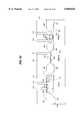
- FIG. 1 depicts a vertically integrated bipolar device design commonly employed in the prior art, along with the mask levels utilized to form this device;
- FIG. 2 is the vertically integrated bipolar device of FIG. 1 and its equivalent circuit diagram
- FIGS. 3A and 3B depict, for comparison purposes, a prior art bipolar device employing a prior art approach to reducing collector resistance and an exemplary embodiment of the present invention
- FIG. 4 is an illustration of a generic vertically modulated implant layer realized by implanting through two films
- FIG. 5 depicts the final structure of an NPN bipolar device with a vertically modulated subcollector in accordance with a preferred embodiment of the present invention, along with two possible masking layouts for forming the vertically modulated subcollector;
- FIGS. 6-12 illustrate a process flow for forming a vertically modulated subcollector for a bipolar device in accordance with a preferred embodiment of the present invention
- FIGS. 13-19 depict an alternative process flow for forming a vertically modulated subcollector for a bipolar device in accordance with a preferred embodiment of the present invention
- FIGS. 20-27 illustrate a third process flow for forming a vertically modulated subcollector for a bipolar device in accordance with a preferred embodiment of the present invention.
- FIGS. 28-43 depict a fully integrated BiCMOS flow incorporating a vertically modulated subcollector for the bipolar device in accordance with a preferred embodiment of the present invention.
- FIG. 3B a bipolar device in accordance with the preferred embodiment of the present invention is depicted.
- the figures representing device profiles or cross-sections of portions of an integrated circuit during fabrication are not drawn to scale, but instead are drawn so as to illustrate the important features of the invention.
- the process steps and structures described below do not form a complete process flow for manufacturing integrated circuits.
- the present invention may be practiced in conjunction with integrated circuit fabrication techniques currently used in the art, and only so much of the commonly practiced process steps are included as are necessary for an understanding of the present invention.
- a vertically modulated subcollector 304 is employed in FIG. 3B to reduce both the vertical and lateral components of the collector resistance.
- the differential penetration of a high-energy implant creates both a buried layer and its connection to the collector, simultaneously.
- Collector resistance is significantly reduced without the need for separate process steps forming buried collector and sinker structures.
- the resulting technology has a higher performance-to-price ratio.
- Subcollector 304 in FIG. 3B is a vertically modulated buried layer formed by the high energy implant.
- Subcollector 304 includes a portion beneath the base region 114 which is vertically displaced from the portion of subcollector 304 beneath collector contact region 120. At least the portion of subcollector 304 beneath the base region 114 overlaps or intersects the well forming collector region 112.
- Subcollector 304 is an integral, heavily doped region formed by a single implant.
- Subcollector 110 and sinker 302 in FIG. 3A remain distinct despite overlapping or contacting, and are formed by separate implants. Thus, a danger exists that sinker 302, if not properly implanted, will not contact or overlap subcollector 110. In that event, reduction of collector resistance by sinker 302 is less effective.
- Use of vertically modulated subcollector 304 as shown in FIG. 3B avoids this potential problem.
- FIG. 4 the process for forming a generic vertically modulated implant is illustrated.
- the technique employed is similar to that described in U.S. Pat. No. 5,501,993 to J. Borland entitled Method of Constructing CMOS Vertically Modulated Wells (VMW) by Clustered MeV BILLI (Buried Implanted Layer for Lateral Isolation) Implantation.
- VMW CMOS Vertically Modulated Wells
- BILLI Clustered MeV BILLI (Buried Implanted Layer for Lateral Isolation) Implantation.
- Differential film heights are utilized to modulate the vertical doping profile in a substrate resulting from a single implant.
- a first film 402 and a second film 404, which is not coextensive with first film 402 mask an implant into substrate 406.
- Films 402 and 404 may be photoresist, grown or deposited oxides, nitride, polysilicon, or other suitable implant masking films. A single film having a vertical profile modified by photolithography, etch, or other means may also be used.
- the combination of films modulates implant(s) into substrate 406, resulting in a vertically-modulated implant layer 408.
- Impurities of different conductivity types may be implanted.
- Donor (n-type) impurities such as phosphorous or arsenic and acceptor (p-type) impurities such as boron may be implanted through the films, as well as neutral impurities such as silicon or germanium.
- Substrate 406 may be any type of suitable substrate such as a semiconductor crystal (monocrystalline substrate), a substrate with epitaxial layers or doped regions, or a semiconductor-on-insulator (SOI) substrate.
- SOI semiconductor-on-insulator
- the dose or concentration and the implantation energy required to form buried layer 408 will depend on a variety of factors known to those skilled in the art, including the materials used for films 402 and 404, the thickness of films 402 and 404, and the impurity being implanted. By selecting the implant energy and the material, position, and thickness of films 402 and 404 appropriately, the doping profile of buried layer 408 may be tailored to device requirements. Implanted impurities passing through a region 412 in which substrate 406 is exposed (or covered only by a thin oxide 410) results in a portion 414 of buried layer 408 with the deepest implantation depth.
- impurities from the same implant form a portion 418 of buried layer 408 which is somewhat shallower. Both portions 414 and 418 of buried layer 408 are formed by a single implant, using a single dose and energy. A fringe effect of the implantation causes buried layer 408 to smoothly transition 420 between the deepest portion 414 and the shallower portion 418.
- implanted impurities are implanted to the shallowest portion 424 of buried layer 408.
- the material or thickness of film 404 may be selected so as to prevent impurities from reaching substrate 406, forming the shallowest portion 424 of buried layer 408 within film 402 or film 404. Films 402 and 404 may then be subsequently removed, and with them the shallowest portion 424 of implanted layer 408.
- Films 402 and 404 may be different materials selected for different penetration rates by the implant species, or may simply be different layers of the same material. Although the depicted example employs two films for the implantation mask, a single film may be sufficient or three or more films may be used, depending on the implementation.
- a bilevel implanted layer may be formed with an implantation mask of a single film, covering and exposing selected portions of the substrate. The edge of a film, or the transition between regions where the substrate is covered and exposed, may be a single step, multiple steps, a taper, or any other suitable geometry. Variations in film materials and profiles are limited only by processing constraints.
- FIG. 5 the final structure of an NPN bipolar device with a vertically modulated subcollector in accordance with a preferred embodiment of the present invention is depicted, along with two possible masking layouts.
- Vertically modulated subcollector 502 an integral, heavily doped buried layer, contacts or overlaps the collector contact region 504, reducing collector resistance in the vertically integrated NPN device 500.
- Subcollector 502 overlaps collector 506 at least in a portion 508 of subcollector 502 underlying base 510. Another portion 509 of subcollector 502 is vertically displaced from the portion 508 underlying base 510.
- the semiconductor body in which bipolar device 500 is formed comprises a monocrystalline, heavily doped substrate 512 on which a lightly doped epitaxial layer 514 was grown or deposited.
- CMOS devices by comparison, tolerate a fairly limited number of process variations.
- An illustrative sample of the process flows capable of forming the NPN bipolar device of FIG. 5 are described below, although it will be understood that others are possible. All flows described are illustrated as being formed on bulk silicon wafers. However, the same flows will work on other substrates as well, such as bulk substrates with a deposited layer of high resistivity epitaxial silicon.
- Either mask sequence 550 or 552 depicted in FIG. 5 may be used, depending on the process flow employed.
- the process flows described in conjunction with FIGS. 6-12 and FIGS. 13-19 utilizes mask sequence 550, while the process flow described in conjunction with FIGS. 20-27 utilize mask sequence 552.
- FIGS. 6-12 a process flow for forming a vertically modulated subcollector in accordance with a preferred embodiment of the present invention is illustrated, along with the mask levels used in the process.
- mask sequence 550 from FIG. 5 is used with the collector mask initially used in a dark field mode. If positive resist is being used, in a clear field mode, islands of photoresist remain only where the mask is opaque. In dark field mode, openings in photoresist are formed in regions where the mask is NOT opaque. Clear field shapes leave islands of resist, whereas Dark field shapes leave holes in resist.
- a support/screen oxide 602 is first grown on substrate 604, followed by deposition of silicon nitride layer 606, preferably by a furnace LPCVD.
- Substrate 604 is a lightly doped p-substrate in the depicted example.
- a layer of photoresist 608 is deposited and patterned with the collector mask 609 to etch a window 610 in silicon nitride 606.
- photoresist layer 608 is removed. As depicted in FIG. 8, a new photoresist layer 612 is deposited and patterned using base mask 613 to form a window 614 defining the base region. Opening 614 in photoresist layer 612 is smaller than opening 610 in silicon nitride 606. A high energy implant using a suitable donor species (arsenic, phosphorous, antimony, etc.) is then performed to form vertically modulated buried n+ region 616 for the subcollector. Photoresist layer 612 and silicon nitride layer 606 modulate the vertical doping profile resulting from the implant.
- a suitable donor species arsenic, phosphorous, antimony, etc.
- photoresist layer 612 thickness, silicon nitride layer 606 thickness, and implant conditions may be modified to control the buried n+ layer doping profile. It may be preferable to adjust these variables so that, outside the region defined by the collector mask, the doping profile of the n+ region lies within the silicon nitride layer 606 and may be subsequently removed.
- n-well 618 for the collector.
- n-well 618 which forms the collector, overlaps or intersects only part of that portion of buried n+ layer 616 which will form the subcollector.
- the same photoresist layer 612 with the patterned window 614 may be used to implant p-region 620 for the base.
- Photoresist 612 and silicon nitride 606 are then removed.
- a second layer of silicon nitride 622 is deposited and patterned using collector mask 609 in a clear field mode.
- silicon nitride layer 622 is deposited over the portion of substrate 604 which was previously exposed by opening 610 in silicon nitride layer 606, now removed.
- Field oxide 624 is then grown as depicted in FIG. 11, over regions of substrate 604 where nitride layer 622 is absent.
- Nitride 622 and oxide 624 are then stripped as illustrated in FIG. 12. The process steps depicted in FIGS.
- the resulting structure includes vertically modulated buried layer 616 in substrate 604, a portion of which underlies base region 620.
- Collector well 618 overlaps at least the portion of buried layer 616 underlying base 620. From this point, the substrate may be processed on a typical CMOS process route to form a BiCMOS integrated circuit.
- FIGS. 13-19 an alternative process flow for forming a vertically modulated subcollector in accordance with a preferred embodiment of the present invention is depicted, along with the mask levels used in the process.
- mask sequence 550 from FIG. 5 is used with the collector mask initially used in a clear field mode.
- the process begins with a substrate 702 on which a support/screen oxide 704 is grown and a silicon nitride layer 706 deposited as illustrated in FIG. 13.
- Substrate 702 is a lightly doped p-substrate in this depicted example.
- a layer of photoresist 708 is deposited and patterned using the collector mask 710, followed by an etch leaving an island of silicon nitride 707.
- Photoresist 708 is then removed and a well oxide/field oxide 712 grown over substrate 702 in regions which are not protected by nitride island 707, followed by removal of the nitride island 707 as illustrated in FIG. 15.
- An opening 713 through well oxide 712 remains in the region protected by nitride layer 707.
- a new layer of photoresist 714 is deposited and patterned using base mask 716 to define a window 718 for the base region.
- Window 718 in photoresist 714 is smaller than opening 713 in well oxide 712.
- a high energy implant of a suitable donor species forms buried n+ layer 720, vertically modulated by photoresist 714 and well oxide 712.
- the thicknesses of photoresist 714 and well oxide 712, together with the implant conditions, may be adjusted to control the doping profile of buried n+ layer 720. It may be desirable to tailor these variables so that, outside the region defined by collector mask 710 and nitride island 707, the doping profile of n+ layer 720 lies within well oxide 712 as shown and may be subsequently removed.
- n-well 722 for the collector and p-region 724 for the base may be formed using n-well 722 for the collector and p-region 724 for the base, as depicted in FIG. 17.
- implant of p-region 724 may be deferred until a later point in the process flow, when photo masking operations using base mask 716 may be repeated.
- Photoresist 714, support oxide 704, and well oxide 712 are then removed as illustrated in FIG. 18.
- Well oxide 712 is preferably removed in a solution of hydrofluoric acid.
- the n+ doping profile within well oxide 712 is simultaneously removed. As with the previous process flow, this results in a structure in which collector well 722 only overlaps the portion of buried layer 720 underlying 724.
- the substrate may be processed in a typical CMOS process route to produce a BICMOS product.
- FIG. 19 illustrates this progression, where the substrate has been processed through a "zero level" oxidation typically used at the start of a CMOS process to form support/screen oxide 726.
- FIGS. 20-27 a third process flow for forming a vertically modulated subcollector for a bipolar device in accordance with a preferred embodiment of the present invention is depicted, along with the mask levels used in the process.
- mask sequence 552 from FIG. 5 is used, this time with the collector mask initially used in a dark field mode.
- the process flow of FIGS. 20-27 represents a tighter integration of CMOS and NPN bipolar processing than the two previous process flows described.
- the process begins with a substrate 800, on which a support/screen oxide 802 is grown.
- Substrate 800 is again a lightly doped p-substrate in this depicted embodiment.
- a layer of photoresist 804 is deposited and patterned using collector mask 806, as depicted in FIG. 21.
- a high-energy implant of a suitable donor species is then performed, vertically modulated by photoresist 804 and opening 805 through photoresist 804, to form buried n+ layer 808.
- a single layer implantation mask is sufficient to form the bilevel buried layer 808 required to form a vertically modulated subcollector in accordance with the present invention.
- the thickness of photoresist 804 and the implant conditions may be adjusted to control the vertical doping profile of n+ layer 808.
- a photolithography step to define the collector region is performed. If a suitable photoresist has been used, the step may be performed by reexposing photoresist 804. Otherwise, photoresist 804 is stripped and a new layer of photoresist 810 is deposited. Photoresist 810 is patterned using a n-well mask 812 to form window 814. Opening 814 through photoresist 810 is larger than opening 805 in photoresist 804.
- Performance of the photolithography step forming opening 814 in photoresist 810 may be coincident with the n-well photolithography step of a CMOS process. It is assumed that n-well mask 812 is drawn to a shape derived from the collector mask data. An n-well implant through window 814 in photoresist 810 forms the collector. In this embodiment, collector well 816 overlaps the entire portion of buried layer 808 which will form the subcollector.
- photoresist 810 is stripped and a layer of nitride 818 is deposited, on which is deposited another layer of photoresist 820.
- Photoresist 820 is patterned using p-well mask 819 (which is the opposite of n-well mask 812), and nitride 818 is etched to leave a protective island of nitride over the collector and subcollector.
- a well oxidation is then performed to grow field oxide 822 as illustrated in FIG. 24A.
- a silicon nitride strip/etch and an oxide strip/etch, preferably in acid solutions, follows to remove nitride 818 and oxide 822.
- screen oxide 824 is grown as depicted in FIG. 24B.
- a layer of photoresist 826 is again deposited and patterned using p-well mask 819, followed by implantation of the p-wells 828 as illustrated in FIG. 25.
- the structure is fairly consistent with the product of CMOS front-end processing.
- the flow can now continue with typical CMOS process steps that occur after well formation (i.e., field implant, active formation, field growth, etc.).
- a photoresist layer 830 is deposited and patterned using base mask 832 to allow an implant through window 836 in photoresist 830 of p-region 834 forming the base. Opening 836 in photoresist 830 is smaller than opening 805 in photoresist layer 804. As noted earlier, placement of the base formation step within the process flow is a function of the desired device characteristics. Photoresist 830 is stripped to leave the final structure illustrated in FIG. 27.
- FIGS. 28-43 a fully integrated BiCMOS flow incorporating a vertically modulated subcollector in accordance with a preferred embodiment of the present invention is illustrated.
- the process begins with a substrate 902 on which support oxide 904 is grown and nitride layer 906 is deposited.
- Substrate 902 is a lightly doped p-substrate in the embodiment shown.
- the mask layout 908 used for the process is depicted FIG. 29.
- Photoresist 910 is deposited and patterned, as illustrated in FIG. 30, using collector mask 912 in a clear field mode to define the region of the modulated n+ buried layer.
- Photoresist 910 is removed and a well oxidation performed to grow oxide 914, after which nitride 906 is removed as depicted in FIG. 31.
- a new photoresist layer 916 is deposited and patterned using base mask 918 to form window 920.
- a subsequent implant through window 920 creates the n-well 926 forming the collector.
- An additional implant through window 920 may be performed to form base/p-region 926 as shown, or formation of the base may be optionally deferred until a later point in the process.
- photoresist 916 is stripped and oxide 914 removed, followed by growth of support/screen oxide 928.
- a layer of photoresist 930 is then deposited and patterned using n-well mask 932 to form window 934 through which n-well 936 for PMOS devices is implanted, as illustrated in FIG. 34.
- the n-well 936 formation may be followed by formation of a p-well using the "opposite" mask data of n-well mask 932. Alternatively, a blanket adjust implant may be performed.
- nitride layer 938 is deposited, over which a photoresist 940 is deposited.
- Photoresist 940 is patterned using collector mask 912 and active MOS mask 942.
- Nitride layer 938 is then etched to leave protective islands of nitride over the active regions of the substrate.
- photoresist 940 is stripped and replaced with new photoresist 944.
- Photoresist 944 is patterned using collector region mask 946 and n-well mask 932. Patterned photoresist 944 masks implantation of field implants 948.
- Photoresist 944 is then stripped and field oxide 950 grown, as illustrated in FIGS. 37A-37B.
- Nitride 938 is then removed as depicted in FIG. 38A.
- gate oxide 952 is grown and polysilicon layer 954 deposited as illustrated in FIG. 38B.
- a layer of photoresist 956 is deposited and patterned using poly-1 mask 958, and exposed portions of polysilicon layer 954 are removed.
- active MOS masks 942 are used individually to pattern photoresist (not shown) to mask separate implantation of source/drain regions 960 for the MOS devices.
- emitter region and collector region masks 962 and 964 are used to pattern photoresist (not shown) to mask implantation of the emitter region 966 and collector contact region 968.
- a small gap between collector contact region 968 and subcollector 922 may be acceptable, but preferably collector contact region 968 and subcollector 922 contact or overlap. Implantation of the emitter and collector contact regions 966 and 968 may alternatively be performed before implantation of source/drain regions 960 for the MOS devices.
- FIG. 43 illustrates the final BiCMOS structure through the contact level, including a vertically integrated NPN bipolar transistor with a vertically modulated subcollector in accordance with a preferred embodiment of the present invention and a NMOS and PMOS transistors.
- Bipolar device 976 includes bilevel subcollector 922 with a portion underlying base 926 and overlapping collector 924. That portion is vertically displaced from the remainder of subcollector 922.
- NMOS field effect transistor 978 is deposited in substrate 902 and PMOS field effect transistor 980 is deposited within well 936 within substrate 902.
- Field oxide regions 950 on substrate 902 between NPN bipolar device 976, NMOS transistor 978, and PMOS transistor 980 provide isolation, along with field implant regions 948 beneath field oxide regions 950.
Abstract
Description
Claims (17)
Priority Applications (5)
| Application Number | Priority Date | Filing Date | Title |
|---|---|---|---|
| US08/801,668 US5858828A (en) | 1997-02-18 | 1997-02-18 | Use of MEV implantation to form vertically modulated N+ buried layer in an NPN bipolar transistor |
| PCT/US1998/003520 WO1998036457A1 (en) | 1997-02-18 | 1998-02-17 | Bipolar transistor with reduced vertical collector resistance |
| AU64382/98A AU6438298A (en) | 1997-02-18 | 1998-02-17 | Bipolar transistor with reduced vertical collector resistance |
| TW087102155A TW374248B (en) | 1997-02-18 | 1998-02-17 | Use of MeV implantation to form vertically modulated n+ buried layer in an NPN bipolar transistor |
| US09/272,732 US6316817B1 (en) | 1997-02-18 | 1998-12-14 | MeV implantation to form vertically modulated N+ buried layer in an NPN bipolar transistor |
Applications Claiming Priority (1)
| Application Number | Priority Date | Filing Date | Title |
|---|---|---|---|
| US08/801,668 US5858828A (en) | 1997-02-18 | 1997-02-18 | Use of MEV implantation to form vertically modulated N+ buried layer in an NPN bipolar transistor |
Related Child Applications (1)
| Application Number | Title | Priority Date | Filing Date |
|---|---|---|---|
| US09/272,732 Division US6316817B1 (en) | 1997-02-18 | 1998-12-14 | MeV implantation to form vertically modulated N+ buried layer in an NPN bipolar transistor |
Publications (1)
| Publication Number | Publication Date |
|---|---|
| US5858828A true US5858828A (en) | 1999-01-12 |
Family
ID=25181751
Family Applications (2)
| Application Number | Title | Priority Date | Filing Date |
|---|---|---|---|
| US08/801,668 Expired - Lifetime US5858828A (en) | 1997-02-18 | 1997-02-18 | Use of MEV implantation to form vertically modulated N+ buried layer in an NPN bipolar transistor |
| US09/272,732 Expired - Lifetime US6316817B1 (en) | 1997-02-18 | 1998-12-14 | MeV implantation to form vertically modulated N+ buried layer in an NPN bipolar transistor |
Family Applications After (1)
| Application Number | Title | Priority Date | Filing Date |
|---|---|---|---|
| US09/272,732 Expired - Lifetime US6316817B1 (en) | 1997-02-18 | 1998-12-14 | MeV implantation to form vertically modulated N+ buried layer in an NPN bipolar transistor |
Country Status (4)
| Country | Link |
|---|---|
| US (2) | US5858828A (en) |
| AU (1) | AU6438298A (en) |
| TW (1) | TW374248B (en) |
| WO (1) | WO1998036457A1 (en) |
Cited By (16)
| Publication number | Priority date | Publication date | Assignee | Title |
|---|---|---|---|---|
| US6506656B2 (en) | 2001-03-19 | 2003-01-14 | International Business Machines Corporation | Stepped collector implant and method for fabrication |
| US6656815B2 (en) | 2001-04-04 | 2003-12-02 | International Business Machines Corporation | Process for implanting a deep subcollector with self-aligned photo registration marks |
| US20040267373A1 (en) * | 2003-06-25 | 2004-12-30 | Dwyer Kimberly Ann | Assembly tool for modular implants and associated method |
| US20050033444A1 (en) * | 2003-06-25 | 2005-02-10 | Jones Michael C. | Assembly tool for modular implants and associated method |
| US20050179093A1 (en) * | 2004-02-17 | 2005-08-18 | Silicon Space Technology Corporation | Buried guard ring and radiation hardened isolation structures and fabrication methods |
| US20060264042A1 (en) * | 2005-05-20 | 2006-11-23 | Texas Instruments, Incorporated | Interconnect structure including a silicon oxycarbonitride layer |
| US20070141794A1 (en) * | 2005-10-14 | 2007-06-21 | Silicon Space Technology Corporation | Radiation hardened isolation structures and fabrication methods |
| US7271070B1 (en) * | 1998-09-29 | 2007-09-18 | Hartmut Grutzediek | Method for producing transistors |
| US20080142899A1 (en) * | 2006-08-04 | 2008-06-19 | Silicon Space Technology Corporation | Radiation immunity of integrated circuits using backside die contact and electrically conductive layers |
| US8518050B2 (en) | 2007-10-31 | 2013-08-27 | DePuy Synthes Products, LLC | Modular taper assembly device |
| US8998919B2 (en) | 2003-06-25 | 2015-04-07 | DePuy Synthes Products, LLC | Assembly tool for modular implants, kit and associated method |
| US9095452B2 (en) | 2010-09-01 | 2015-08-04 | DePuy Synthes Products, Inc. | Disassembly tool |
| US9101495B2 (en) | 2010-06-15 | 2015-08-11 | DePuy Synthes Products, Inc. | Spiral assembly tool |
| US9504578B2 (en) | 2011-04-06 | 2016-11-29 | Depuy Synthes Products, Inc | Revision hip prosthesis having an implantable distal stem component |
| US9717545B2 (en) | 2007-10-30 | 2017-08-01 | DePuy Synthes Products, Inc. | Taper disengagement tool |
| US10038058B2 (en) | 2016-05-07 | 2018-07-31 | Silicon Space Technology Corporation | FinFET device structure and method for forming same |
Families Citing this family (1)
| Publication number | Priority date | Publication date | Assignee | Title |
|---|---|---|---|---|
| US7968394B2 (en) * | 2005-12-16 | 2011-06-28 | Freescale Semiconductor, Inc. | Transistor with immersed contacts and methods of forming thereof |
Citations (12)
| Publication number | Priority date | Publication date | Assignee | Title |
|---|---|---|---|---|
| DE3026218A1 (en) * | 1980-07-10 | 1982-02-04 | Siemens AG, 1000 Berlin und 8000 München | Semiconductor with high surface breakdown voltage - has boron implanted channel between base and channel stopper zones of different conductivity |
| US4710477A (en) * | 1983-09-12 | 1987-12-01 | Hughes Aircraft Company | Method for forming latch-up immune, multiple retrograde well high density CMOS FET |
| US4711017A (en) * | 1986-03-03 | 1987-12-08 | Trw Inc. | Formation of buried diffusion devices |
| US4729964A (en) * | 1985-04-15 | 1988-03-08 | Hitachi, Ltd. | Method of forming twin doped regions of the same depth by high energy implant |
| US4732869A (en) * | 1985-07-11 | 1988-03-22 | U.S. Philips Corporation | Method of forming implanted regions in a semiconductor device by use of a three layer masking structure |
| US5121185A (en) * | 1987-10-09 | 1992-06-09 | Hitachi, Ltd. | Monolithic semiconductor IC device including blocks having different functions with different breakdown voltages |
| US5160996A (en) * | 1987-10-08 | 1992-11-03 | Matsushita Electric Industrial Co., Inc. | Structure and method of manufacture for semiconductor device |
| JPH06314663A (en) * | 1993-04-30 | 1994-11-08 | Toyota Motor Corp | Manufacture of semiconductor device |
| US5436176A (en) * | 1990-03-27 | 1995-07-25 | Matsushita Electric Industrial Co., Ltd. | Method for fabricating a semiconductor device by high energy ion implantation while minimizing damage within the semiconductor substrate |
| US5501993A (en) * | 1994-11-22 | 1996-03-26 | Genus, Inc. | Method of constructing CMOS vertically modulated wells (VMW) by clustered MeV BILLI (buried implanted layer for lateral isolation) implantation |
| EP0731387A2 (en) * | 1995-02-16 | 1996-09-11 | Samsung Electronics Co., Ltd. | Gray-tone mask and pattern formation and ion implantation methods using the same |
| DE19611692A1 (en) * | 1996-03-25 | 1997-10-02 | Siemens Ag | Bipolar transistor with high-energy implanted collector and manufacturing process |
Family Cites Families (8)
| Publication number | Priority date | Publication date | Assignee | Title |
|---|---|---|---|---|
| US3397449A (en) * | 1965-07-14 | 1968-08-20 | Hughes Aircraft Co | Making p-nu junction under glass |
| US4812417A (en) * | 1986-07-30 | 1989-03-14 | Mitsubishi Denki Kabushiki Kaisha | Method of making self aligned external and active base regions in I.C. processing |
| JP2509690B2 (en) * | 1989-02-20 | 1996-06-26 | 株式会社東芝 | Semiconductor device |
| JP2947822B2 (en) * | 1989-07-28 | 1999-09-13 | 株式会社日立製作所 | Semiconductor device |
| US5235206A (en) * | 1990-10-24 | 1993-08-10 | International Business Machines Corporation | Vertical bipolar transistor with recessed epitaxially grown intrinsic base region |
| JPH0645340A (en) * | 1991-11-12 | 1994-02-18 | Rohm Co Ltd | Semiconductor device and its manufacture |
| DE69402221T2 (en) * | 1993-01-29 | 1997-08-14 | Nat Semiconductor Corp | Bipolar transistors and their manufacturing processes |
| US5541121A (en) * | 1995-01-30 | 1996-07-30 | Texas Instruments Incorporated | Reduced resistance base contact method for single polysilicon bipolar transistors using extrinsic base diffusion from a diffusion source dielectric layer |
-
1997
- 1997-02-18 US US08/801,668 patent/US5858828A/en not_active Expired - Lifetime
-
1998
- 1998-02-17 TW TW087102155A patent/TW374248B/en not_active IP Right Cessation
- 1998-02-17 WO PCT/US1998/003520 patent/WO1998036457A1/en active Application Filing
- 1998-02-17 AU AU64382/98A patent/AU6438298A/en not_active Abandoned
- 1998-12-14 US US09/272,732 patent/US6316817B1/en not_active Expired - Lifetime
Patent Citations (12)
| Publication number | Priority date | Publication date | Assignee | Title |
|---|---|---|---|---|
| DE3026218A1 (en) * | 1980-07-10 | 1982-02-04 | Siemens AG, 1000 Berlin und 8000 München | Semiconductor with high surface breakdown voltage - has boron implanted channel between base and channel stopper zones of different conductivity |
| US4710477A (en) * | 1983-09-12 | 1987-12-01 | Hughes Aircraft Company | Method for forming latch-up immune, multiple retrograde well high density CMOS FET |
| US4729964A (en) * | 1985-04-15 | 1988-03-08 | Hitachi, Ltd. | Method of forming twin doped regions of the same depth by high energy implant |
| US4732869A (en) * | 1985-07-11 | 1988-03-22 | U.S. Philips Corporation | Method of forming implanted regions in a semiconductor device by use of a three layer masking structure |
| US4711017A (en) * | 1986-03-03 | 1987-12-08 | Trw Inc. | Formation of buried diffusion devices |
| US5160996A (en) * | 1987-10-08 | 1992-11-03 | Matsushita Electric Industrial Co., Inc. | Structure and method of manufacture for semiconductor device |
| US5121185A (en) * | 1987-10-09 | 1992-06-09 | Hitachi, Ltd. | Monolithic semiconductor IC device including blocks having different functions with different breakdown voltages |
| US5436176A (en) * | 1990-03-27 | 1995-07-25 | Matsushita Electric Industrial Co., Ltd. | Method for fabricating a semiconductor device by high energy ion implantation while minimizing damage within the semiconductor substrate |
| JPH06314663A (en) * | 1993-04-30 | 1994-11-08 | Toyota Motor Corp | Manufacture of semiconductor device |
| US5501993A (en) * | 1994-11-22 | 1996-03-26 | Genus, Inc. | Method of constructing CMOS vertically modulated wells (VMW) by clustered MeV BILLI (buried implanted layer for lateral isolation) implantation |
| EP0731387A2 (en) * | 1995-02-16 | 1996-09-11 | Samsung Electronics Co., Ltd. | Gray-tone mask and pattern formation and ion implantation methods using the same |
| DE19611692A1 (en) * | 1996-03-25 | 1997-10-02 | Siemens Ag | Bipolar transistor with high-energy implanted collector and manufacturing process |
Non-Patent Citations (4)
| Title |
|---|
| Characteristics of Bipolar Transistors with Various Depths of n Buried Layers Formed by High Energy Ion Implantation, Akihiro Tamba, Yutaka Kobayashi, Tadeshi Suzuki and Nobuyoshi Natsuaki, Japanese Journal of Applied Physics pp. 156 160, Dec. 1991. * |
| Characteristics of Bipolar Transistors with Various Depths of n+ Buried Layers Formed by High-Energy Ion Implantation, Akihiro Tamba, Yutaka Kobayashi, Tadeshi Suzuki and Nobuyoshi Natsuaki, Japanese Journal of Applied Physics pp. 156-160, Dec. 1991. |
| Tamba A et al: Characteristics of Bipolar Transistors with Various Depth N Buried Layers Formed by High Energy Ion Implantation; Extended Abstracts of the International Conference on Solid State Devices and Materials; Tokyo, Aug. 24 26, 1988; No. Conf. 20, 24 Aug. 1988, Japan Society of Applied Physics; pp. 141 144; XP000042517. * |
| Tamba A et al: Characteristics of Bipolar Transistors with Various Depth N+ Buried Layers Formed by High Energy Ion Implantation; Extended Abstracts of the International Conference on Solid State Devices and Materials; Tokyo, Aug. 24-26, 1988; No. Conf. 20, 24 Aug. 1988, Japan Society of Applied Physics; pp. 141-144; XP000042517. |
Cited By (46)
| Publication number | Priority date | Publication date | Assignee | Title |
|---|---|---|---|---|
| US7271070B1 (en) * | 1998-09-29 | 2007-09-18 | Hartmut Grutzediek | Method for producing transistors |
| US6506656B2 (en) | 2001-03-19 | 2003-01-14 | International Business Machines Corporation | Stepped collector implant and method for fabrication |
| US6656815B2 (en) | 2001-04-04 | 2003-12-02 | International Business Machines Corporation | Process for implanting a deep subcollector with self-aligned photo registration marks |
| US20080091212A1 (en) * | 2003-06-25 | 2008-04-17 | Depuy Products, Inc. | Assembly tool for modular implants and associated method |
| US20040267373A1 (en) * | 2003-06-25 | 2004-12-30 | Dwyer Kimberly Ann | Assembly tool for modular implants and associated method |
| US20050033444A1 (en) * | 2003-06-25 | 2005-02-10 | Jones Michael C. | Assembly tool for modular implants and associated method |
| US8419799B2 (en) | 2003-06-25 | 2013-04-16 | Depuy Products, Inc. | Assembly tool for modular implants and associated method |
| US9381097B2 (en) | 2003-06-25 | 2016-07-05 | DePuy Synthes Products, Inc. | Assembly tool for modular implants, kit and associated method |
| US8998919B2 (en) | 2003-06-25 | 2015-04-07 | DePuy Synthes Products, LLC | Assembly tool for modular implants, kit and associated method |
| US8685036B2 (en) | 2003-06-25 | 2014-04-01 | Michael C. Jones | Assembly tool for modular implants and associated method |
| US20080073725A1 (en) * | 2004-02-17 | 2008-03-27 | Morris Wesley H | Buried guard ring structures and fabrication methods |
| US8497195B2 (en) | 2004-02-17 | 2013-07-30 | Silicon Space Technology Corporation | Method for radiation hardening a semiconductor device |
| US8729640B2 (en) | 2004-02-17 | 2014-05-20 | Silicon Space Technology Corporation | Method and structure for radiation hardening a semiconductor device |
| US20080188045A1 (en) * | 2004-02-17 | 2008-08-07 | Morris Wesley H | Methods for operating and fabricating a semiconductor device having a buried guard ring structure |
| US7629654B2 (en) | 2004-02-17 | 2009-12-08 | Silicon Space Technology Corp. | Buried guard ring structures and fabrication methods |
| US7804138B2 (en) | 2004-02-17 | 2010-09-28 | Silicon Space Technology Corp. | Buried guard ring and radiation hardened isolation structures and fabrication methods |
| US7304354B2 (en) | 2004-02-17 | 2007-12-04 | Silicon Space Technology Corp. | Buried guard ring and radiation hardened isolation structures and fabrication methods |
| US8093145B2 (en) | 2004-02-17 | 2012-01-10 | Silicon Space Technology Corp. | Methods for operating and fabricating a semiconductor device having a buried guard ring structure |
| US20060249759A1 (en) * | 2004-02-17 | 2006-11-09 | Morris Wesley H | Buried guard ring and radiation hardened isolation structures and fabrication methods |
| US20050179093A1 (en) * | 2004-02-17 | 2005-08-18 | Silicon Space Technology Corporation | Buried guard ring and radiation hardened isolation structures and fabrication methods |
| US20060264042A1 (en) * | 2005-05-20 | 2006-11-23 | Texas Instruments, Incorporated | Interconnect structure including a silicon oxycarbonitride layer |
| US8252642B2 (en) | 2005-10-14 | 2012-08-28 | Silicon Space Technology Corp. | Fabrication methods for radiation hardened isolation structures |
| US8278719B2 (en) | 2005-10-14 | 2012-10-02 | Silicon Space Technology Corp. | Radiation hardened isolation structures and fabrication methods |
| US20100267212A1 (en) * | 2005-10-14 | 2010-10-21 | Morris Wesley H | Fabrication methods for radiation hardened isolation structures |
| US20070141794A1 (en) * | 2005-10-14 | 2007-06-21 | Silicon Space Technology Corporation | Radiation hardened isolation structures and fabrication methods |
| US20080142899A1 (en) * | 2006-08-04 | 2008-06-19 | Silicon Space Technology Corporation | Radiation immunity of integrated circuits using backside die contact and electrically conductive layers |
| US9717545B2 (en) | 2007-10-30 | 2017-08-01 | DePuy Synthes Products, Inc. | Taper disengagement tool |
| US8518050B2 (en) | 2007-10-31 | 2013-08-27 | DePuy Synthes Products, LLC | Modular taper assembly device |
| US9119601B2 (en) | 2007-10-31 | 2015-09-01 | DePuy Synthes Products, Inc. | Modular taper assembly device |
| US10166118B2 (en) | 2010-06-15 | 2019-01-01 | DePuy Synthes Products, Inc. | Spiral assembly tool |
| US9101495B2 (en) | 2010-06-15 | 2015-08-11 | DePuy Synthes Products, Inc. | Spiral assembly tool |
| US10292837B2 (en) | 2010-09-01 | 2019-05-21 | Depuy Synthes Products Inc. | Disassembly tool |
| US9867720B2 (en) | 2010-09-01 | 2018-01-16 | DePuy Synthes Products, Inc. | Disassembly tool |
| US9095452B2 (en) | 2010-09-01 | 2015-08-04 | DePuy Synthes Products, Inc. | Disassembly tool |
| US9597188B2 (en) | 2011-04-06 | 2017-03-21 | DePuy Synthes Products, Inc. | Version-replicating instrument and orthopaedic surgical procedure for using the same to implant a revision hip prosthesis |
| US9949833B2 (en) | 2011-04-06 | 2018-04-24 | DePuy Synthes Products, Inc. | Finishing RASP and orthopaedic surgical procedure for using the same to implant a revision hip prosthesis |
| US10064725B2 (en) | 2011-04-06 | 2018-09-04 | DePuy Synthes Products, Inc. | Distal reamer for use during an orthopaedic surgical procedure to implant a revision hip prosthesis |
| US9737405B2 (en) | 2011-04-06 | 2017-08-22 | DePuy Synthes Products, Inc. | Orthopaedic surgical procedure for implanting a revision hip prosthesis |
| US10226345B2 (en) | 2011-04-06 | 2019-03-12 | DePuy Synthes Products, Inc. | Version-replicating instrument and orthopaedic surgical procedure for using the same to implant a revision hip prosthesis |
| US9504578B2 (en) | 2011-04-06 | 2016-11-29 | Depuy Synthes Products, Inc | Revision hip prosthesis having an implantable distal stem component |
| US10603173B2 (en) | 2011-04-06 | 2020-03-31 | DePuy Synthes Products, Inc. | Orthopaedic surgical procedure for implanting a revision hip prosthesis |
| US10772730B2 (en) | 2011-04-06 | 2020-09-15 | DePuy Synthes Products, Inc. | Finishing rasp and orthopaedic surgical procedure for using the same to implant a revision hip prosthesis |
| US10888427B2 (en) | 2011-04-06 | 2021-01-12 | DePuy Synthes Products, Inc. | Distal reamer for use during an orthopaedic surgical procedure to implant a revision hip prosthesis |
| US10925739B2 (en) | 2011-04-06 | 2021-02-23 | DePuy Synthes Products, Inc. | Version-replicating instrument and orthopaedic surgical procedure for using the same to implant a revision hip prosthesis |
| US10038058B2 (en) | 2016-05-07 | 2018-07-31 | Silicon Space Technology Corporation | FinFET device structure and method for forming same |
| US10615260B1 (en) | 2016-05-07 | 2020-04-07 | Silicon Space Technology Corporation | Method for forming FinFET device structure |
Also Published As
| Publication number | Publication date |
|---|---|
| WO1998036457A1 (en) | 1998-08-20 |
| US6316817B1 (en) | 2001-11-13 |
| AU6438298A (en) | 1998-09-08 |
| TW374248B (en) | 1999-11-11 |
Similar Documents
| Publication | Publication Date | Title |
|---|---|---|
| US5326710A (en) | Process for fabricating lateral PNP transistor structure and BICMOS IC | |
| US5856003A (en) | Method for forming pseudo buried layer for sub-micron bipolar or BiCMOS device | |
| US5858828A (en) | Use of MEV implantation to form vertically modulated N+ buried layer in an NPN bipolar transistor | |
| US5294823A (en) | SOI BICMOS process | |
| US5846868A (en) | Method for forming a walled-emitter transistor | |
| KR0139805B1 (en) | Method of making single polysilicon self-aligned transistor | |
| US4902639A (en) | Process for making BiCMOS integrated circuit having a shallow trench bipolar transistor with vertical base contacts | |
| US5323057A (en) | Lateral bipolar transistor with insulating trenches | |
| US4874714A (en) | Method of making laterally oriented Schottky diode | |
| JPS5929153B2 (en) | Method of forming low resistance interconnects in MOS n-channel silicon gate integrated circuits | |
| US5556796A (en) | Self-alignment technique for forming junction isolation and wells | |
| EP0500233A2 (en) | Bipolar transistor structure & BICMOS IC fabrication process | |
| JP2824263B2 (en) | High voltage merged bipolar / CMOS integrated circuit | |
| US5328859A (en) | Method of making high voltage PNP bipolar transistor in CMOS | |
| EP0476571A2 (en) | Semiconductor device with vertical bipolar transistors | |
| US5994190A (en) | Semiconductor device with impurity layer as channel stopper immediately under silicon oxide film | |
| EP0600596B1 (en) | Improved bipolar transistor | |
| JPH04343434A (en) | Manufacture of semiconductor device | |
| US5065209A (en) | Bipolar transistor fabrication utilizing CMOS techniques | |
| KR930005508B1 (en) | Semiconductor device and manufacturing method of the same | |
| US5453387A (en) | Fabrication method of semiconductor device with neighboring n- and p-type regions | |
| JP3244534B2 (en) | Manufacturing method of MOS integrated circuit | |
| US5789789A (en) | Semiconductor device and manufacturing method for improved voltage resistance between an N-well and N-type diffusion layer | |
| KR0175378B1 (en) | Lateral bipolar transistor and method of manufacturing the same | |
| KR100346822B1 (en) | A method for fabrication of semiconductor devices comprising bipolar transistor and resistors |
Legal Events
| Date | Code | Title | Description |
|---|---|---|---|
| AS | Assignment |
Owner name: SYMBIOS LOGIC INC., COLORADO Free format text: ASSIGNMENT OF ASSIGNORS INTEREST;ASSIGNORS:SELISKAR, JOHN J.;DANIEL, DAVID W.;RANDAZZO, TODD A.;REEL/FRAME:008546/0841 Effective date: 19970213 |
|
| AS | Assignment |
Owner name: SYMBIOS, INC ., COLORADO Free format text: CHANGE OF NAME;ASSIGNOR:SYMBIOS LOGIC INC.;REEL/FRAME:009089/0936 Effective date: 19971210 |
|
| AS | Assignment |
Owner name: LSI LOGIC CORPORATION, CALIFORNIA Free format text: ASSIGNMENT OF ASSIGNORS INTEREST;ASSIGNOR:SYMBIOS, INC.;REEL/FRAME:009500/0554 Effective date: 19980922 |
|
| AS | Assignment |
Owner name: LEHMAN COMMERCIAL PAPER INC., AS ADMINISTRATIVE AG Free format text: SECURITY AGREEMENT;ASSIGNORS:HYUNDAI ELECTRONICS AMERICA, A CORP. OF CALIFORNIA;SYMBIOS, INC., A CORP. OF DELAWARE;REEL/FRAME:009396/0441 Effective date: 19980226 |
|
| STCF | Information on status: patent grant |
Free format text: PATENTED CASE |
|
| FPAY | Fee payment |
Year of fee payment: 4 |
|
| FEPP | Fee payment procedure |
Free format text: PAT HOLDER NO LONGER CLAIMS SMALL ENTITY STATUS, ENTITY STATUS SET TO UNDISCOUNTED (ORIGINAL EVENT CODE: STOL); ENTITY STATUS OF PATENT OWNER: LARGE ENTITY |
|
| AS | Assignment |
Owner name: SYMBIOS, INC., COLORADO Free format text: RELEASE OF SECURITY INTEREST;ASSIGNOR:LEHMAN COMMERICAL PAPER INC.;REEL/FRAME:016602/0895 Effective date: 20050107 Owner name: HYUNDAI ELECTRONICS AMERICA, CALIFORNIA Free format text: RELEASE OF SECURITY INTEREST;ASSIGNOR:LEHMAN COMMERICAL PAPER INC.;REEL/FRAME:016602/0895 Effective date: 20050107 |
|
| REMI | Maintenance fee reminder mailed | ||
| FPAY | Fee payment |
Year of fee payment: 8 |
|
| SULP | Surcharge for late payment |
Year of fee payment: 7 |
|
| FEPP | Fee payment procedure |
Free format text: PAYER NUMBER DE-ASSIGNED (ORIGINAL EVENT CODE: RMPN); ENTITY STATUS OF PATENT OWNER: LARGE ENTITY Free format text: PAYOR NUMBER ASSIGNED (ORIGINAL EVENT CODE: ASPN); ENTITY STATUS OF PATENT OWNER: LARGE ENTITY |
|
| FPAY | Fee payment |
Year of fee payment: 12 |
|
| AS | Assignment |
Owner name: DEUTSCHE BANK AG NEW YORK BRANCH, AS COLLATERAL AG Free format text: PATENT SECURITY AGREEMENT;ASSIGNORS:LSI CORPORATION;AGERE SYSTEMS LLC;REEL/FRAME:032856/0031 Effective date: 20140506 |
|
| AS | Assignment |
Owner name: LSI CORPORATION, CALIFORNIA Free format text: CHANGE OF NAME;ASSIGNOR:LSI LOGIC CORPORATION;REEL/FRAME:033102/0270 Effective date: 20070406 |
|
| AS | Assignment |
Owner name: AVAGO TECHNOLOGIES GENERAL IP (SINGAPORE) PTE. LTD Free format text: ASSIGNMENT OF ASSIGNORS INTEREST;ASSIGNOR:LSI CORPORATION;REEL/FRAME:035058/0248 Effective date: 20140804 |
|
| AS | Assignment |
Owner name: LSI CORPORATION, CALIFORNIA Free format text: TERMINATION AND RELEASE OF SECURITY INTEREST IN PATENT RIGHTS (RELEASES RF 032856-0031);ASSIGNOR:DEUTSCHE BANK AG NEW YORK BRANCH, AS COLLATERAL AGENT;REEL/FRAME:037684/0039 Effective date: 20160201 Owner name: AGERE SYSTEMS LLC, PENNSYLVANIA Free format text: TERMINATION AND RELEASE OF SECURITY INTEREST IN PATENT RIGHTS (RELEASES RF 032856-0031);ASSIGNOR:DEUTSCHE BANK AG NEW YORK BRANCH, AS COLLATERAL AGENT;REEL/FRAME:037684/0039 Effective date: 20160201 |
|
| AS | Assignment |
Owner name: BANK OF AMERICA, N.A., AS COLLATERAL AGENT, NORTH CAROLINA Free format text: PATENT SECURITY AGREEMENT;ASSIGNOR:AVAGO TECHNOLOGIES GENERAL IP (SINGAPORE) PTE. LTD.;REEL/FRAME:037808/0001 Effective date: 20160201 Owner name: BANK OF AMERICA, N.A., AS COLLATERAL AGENT, NORTH Free format text: PATENT SECURITY AGREEMENT;ASSIGNOR:AVAGO TECHNOLOGIES GENERAL IP (SINGAPORE) PTE. LTD.;REEL/FRAME:037808/0001 Effective date: 20160201 |
|
| AS | Assignment |
Owner name: AVAGO TECHNOLOGIES GENERAL IP (SINGAPORE) PTE. LTD., SINGAPORE Free format text: TERMINATION AND RELEASE OF SECURITY INTEREST IN PATENTS;ASSIGNOR:BANK OF AMERICA, N.A., AS COLLATERAL AGENT;REEL/FRAME:041710/0001 Effective date: 20170119 Owner name: AVAGO TECHNOLOGIES GENERAL IP (SINGAPORE) PTE. LTD Free format text: TERMINATION AND RELEASE OF SECURITY INTEREST IN PATENTS;ASSIGNOR:BANK OF AMERICA, N.A., AS COLLATERAL AGENT;REEL/FRAME:041710/0001 Effective date: 20170119 |
|
| AS | Assignment |
Owner name: BELL SEMICONDUCTOR, LLC, ILLINOIS Free format text: ASSIGNMENT OF ASSIGNORS INTEREST;ASSIGNORS:AVAGO TECHNOLOGIES GENERAL IP (SINGAPORE) PTE. LTD.;BROADCOM CORPORATION;REEL/FRAME:044886/0608 Effective date: 20171208 |
|
| AS | Assignment |
Owner name: CORTLAND CAPITAL MARKET SERVICES LLC, AS COLLATERA Free format text: SECURITY INTEREST;ASSIGNORS:HILCO PATENT ACQUISITION 56, LLC;BELL SEMICONDUCTOR, LLC;BELL NORTHERN RESEARCH, LLC;REEL/FRAME:045216/0020 Effective date: 20180124 |
|
| AS | Assignment |
Owner name: BELL NORTHERN RESEARCH, LLC, ILLINOIS Free format text: RELEASE BY SECURED PARTY;ASSIGNOR:CORTLAND CAPITAL MARKET SERVICES LLC;REEL/FRAME:059720/0719 Effective date: 20220401 Owner name: BELL SEMICONDUCTOR, LLC, ILLINOIS Free format text: RELEASE BY SECURED PARTY;ASSIGNOR:CORTLAND CAPITAL MARKET SERVICES LLC;REEL/FRAME:059720/0719 Effective date: 20220401 Owner name: HILCO PATENT ACQUISITION 56, LLC, ILLINOIS Free format text: RELEASE BY SECURED PARTY;ASSIGNOR:CORTLAND CAPITAL MARKET SERVICES LLC;REEL/FRAME:059720/0719 Effective date: 20220401 |