US5859446A - Diode and power converting apparatus - Google Patents
Diode and power converting apparatus Download PDFInfo
- Publication number
- US5859446A US5859446A US08/802,882 US80288297A US5859446A US 5859446 A US5859446 A US 5859446A US 80288297 A US80288297 A US 80288297A US 5859446 A US5859446 A US 5859446A
- Authority
- US
- United States
- Prior art keywords
- semiconductor layer
- junction
- diode
- main electrode
- conductivity type
- Prior art date
- Legal status (The legal status is an assumption and is not a legal conclusion. Google has not performed a legal analysis and makes no representation as to the accuracy of the status listed.)
- Expired - Lifetime
Links
- 239000004065 semiconductor Substances 0.000 claims abstract description 174
- 238000009792 diffusion process Methods 0.000 claims abstract description 19
- 239000000969 carrier Substances 0.000 claims description 14
- 239000012535 impurity Substances 0.000 claims description 7
- 238000011084 recovery Methods 0.000 description 30
- 230000007423 decrease Effects 0.000 description 9
- 230000015556 catabolic process Effects 0.000 description 6
- 238000010586 diagram Methods 0.000 description 5
- 230000006698 induction Effects 0.000 description 5
- 238000004904 shortening Methods 0.000 description 4
- 239000003990 capacitor Substances 0.000 description 3
- 238000006243 chemical reaction Methods 0.000 description 3
- 230000001419 dependent effect Effects 0.000 description 3
- 230000000694 effects Effects 0.000 description 3
- 238000002347 injection Methods 0.000 description 3
- 239000007924 injection Substances 0.000 description 3
- 238000000034 method Methods 0.000 description 3
- 230000002093 peripheral effect Effects 0.000 description 3
- 230000001681 protective effect Effects 0.000 description 3
- 229910000789 Aluminium-silicon alloy Inorganic materials 0.000 description 2
- 239000008186 active pharmaceutical agent Substances 0.000 description 2
- 238000002474 experimental method Methods 0.000 description 2
- 229910020489 SiO3 Inorganic materials 0.000 description 1
- 238000001816 cooling Methods 0.000 description 1
- 230000006378 damage Effects 0.000 description 1
- 230000003247 decreasing effect Effects 0.000 description 1
- 238000007599 discharging Methods 0.000 description 1
- 230000005684 electric field Effects 0.000 description 1
- 238000010894 electron beam technology Methods 0.000 description 1
- 238000010438 heat treatment Methods 0.000 description 1
- 238000003780 insertion Methods 0.000 description 1
- 230000037431 insertion Effects 0.000 description 1
- 230000001737 promoting effect Effects 0.000 description 1
- 238000005215 recombination Methods 0.000 description 1
- 230000006798 recombination Effects 0.000 description 1
Images


Classifications
-
- H—ELECTRICITY
- H01—ELECTRIC ELEMENTS
- H01L—SEMICONDUCTOR DEVICES NOT COVERED BY CLASS H10
- H01L29/00—Semiconductor devices adapted for rectifying, amplifying, oscillating or switching, or capacitors or resistors with at least one potential-jump barrier or surface barrier, e.g. PN junction depletion layer or carrier concentration layer; Details of semiconductor bodies or of electrodes thereof ; Multistep manufacturing processes therefor
- H01L29/40—Electrodes ; Multistep manufacturing processes therefor
- H01L29/41—Electrodes ; Multistep manufacturing processes therefor characterised by their shape, relative sizes or dispositions
- H01L29/417—Electrodes ; Multistep manufacturing processes therefor characterised by their shape, relative sizes or dispositions carrying the current to be rectified, amplified or switched
-
- H—ELECTRICITY
- H01—ELECTRIC ELEMENTS
- H01L—SEMICONDUCTOR DEVICES NOT COVERED BY CLASS H10
- H01L29/00—Semiconductor devices adapted for rectifying, amplifying, oscillating or switching, or capacitors or resistors with at least one potential-jump barrier or surface barrier, e.g. PN junction depletion layer or carrier concentration layer; Details of semiconductor bodies or of electrodes thereof ; Multistep manufacturing processes therefor
- H01L29/66—Types of semiconductor device ; Multistep manufacturing processes therefor
- H01L29/86—Types of semiconductor device ; Multistep manufacturing processes therefor controllable only by variation of the electric current supplied, or only the electric potential applied, to one or more of the electrodes carrying the current to be rectified, amplified, oscillated or switched
- H01L29/861—Diodes
- H01L29/8611—Planar PN junction diodes
Definitions
- a reverse current flows for a while. This is because the reverse voltage causes the carriers stored in the diode to be discharged outside due to the conductivity modulation of the carriers.
- This reverse current is known as the recovery current of a diode.
- the peak value (I rp ) of the recovery current increases as the time variation (di/dt) of the current becomes abrupt in a change from the forward to the reverse direction.
- the diode breaks down when di/dt increases excessively at the time of recovery.
- the value of di/dt at which the breakdown occurs (hereinafter called the "critical di/dt") is required to be large.
- critical di/dt di/dt at which the breakdown occurs
- the turn-on time of the switching element needs to be extended to decrease the di/dt in the diode by slowing down the switching speed of the switching element, which would make it necessary to limit the switching frequency and incur an additional cost for cooling the elements because the turn-on loss of the elements increases.
- An object of the present invention which is made in view of the foregoing problems, is to provide a diode designed to improve its critical di/dt and a power converting apparatus adapted to the requirement for improvement in conversion efficiency and cost reduction.
- a diode according to the present invention has a first and a second semiconductor layer for forming the p-n junction, and a first and a second main electrode are connected to the first and second semiconductor layers, respectively. Further, the diode has means for reducing the concentration of the carriers injected from the end portion of the second semiconductor layer in the planar direction.
- the distance between a contact area and the p-n junction region between the first and second semiconductor layers is increased, the contact area being positioned between the second semiconductor layer and the second main electrode.
- a region where the second main electrode and the second semiconductor layer do not contact each other in the end portion of the second semiconductor layer is widened.
- the quantity of the carriers injected into a termination region adjacent to the end portion of the second semiconductor layer is reduced because the resistance of the region where the second main electrode and the second semiconductor layer do not contact each other is greater than that of the second main electrode. Therefore, local current concentration in the end portion of the second semiconductor layer at the time of recovery is prevented. Consequently, the diode will hardly break down at the time of recovery, and the critical di/dt is improved.
- the carrier life time in the vicinity of the termination region of the diode is made shorter than that in an active region, whereby the carriers stored in the first semiconductor layer in the vicinity of the termination region are reduced because the recombination of carriers in the termination region is accelerated. Therefore, local current concentration in the end portion of the second semiconductor layer at the time of recovery is prevented,.and the critical di/dt is improved.
- a power converting apparatus having a parallel circuit including switching elements, such as IGBTs and diodes embodying the present invention has the feature that the di/dt of a current flowing through the diode when the switching element is turned on/off can be increased up to at least 2500 A/ ⁇ s.
- an anode reactor necessary for the power converting apparatus may be reduced in size or dispensed with.
- a protective circuit, such as a snubber circuit may also be reduced in size. Therefore, the power converting apparatus can be reduced in size and weight, and the conversion efficiency can be improved as well.
- a power converting apparatus comprising a plurality of modules in a withstand voltage class of 4000 V or higher, the module having a built-in parallel circuit having switching circuits and diodes without the provision of a reactor.
- the power converting apparatus thus arranged makes it feasible to reduce the size and weight of a large capacity converting apparatus which is used with a high-voltage power supply at a source voltage of about 1500 V or higher.
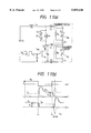
- FIG. 1 is a perspective view of a planar diode embodying the present invention.
- FIG. 2 is a graph showing the relation between L and a critical di/dt in the diode of FIG. 1.
- FIG. 3 is a graph showing the relationship between a forward voltage V F at a current density of 100 A/cm 2 and the ratio between the diffusion length L P of the holes in a semiconductor layer of an n - conductivity type and the thickness Wn - of the semiconductor layer.
- FIG. 4(a) to FIG. 4(c) are diagrams showing the results of experiments made by the present inventors, wherein FIG. 4(a) shows current and voltage waveforms at the time of recovery, and FIG. 4(b) and FIG. 4(c) show the current distribution in the diode.
- FIG. 5(a) and FIG. 5(b) are diagrams illustrating another embodiment of the present invention.
- FIG. 6 is a diagrammatic sectional view illustrating still another embodiment of the present invention.
- FIG. 7 is a diagrammatic sectional view illustrating still another embodiment of the present invention.
- FIG. 8 is a diagrammatic sectional view of still another embodiment of the present invention.
- FIG. 9(a) and FIG. 9(b) are diagrammatic sectional views illustrating the operation of shortening a part of carrier life time in the thickness direction of a diode.
- FIG. 10 is a schematic circuit diagram of an example of a power converting apparatus using the diodes according to the embodiment of the present invention.
- FIG. 11(a) is a schematic circuit diagram and FIG. 11(b) is a waveform diagram illustrating the operation of the inverter of FIG. 10.
- FIG. 1 is a perspective view of a planar diode embodying the present invention.
- a semiconductor layer 12 of the p + conductivity type provided partly in a termination region serves to spread the depletion layer extending from the junction J1 between the semiconductor layer 11 of the p + conductivity type and the semiconductor layer 14 of the n - conductivity type to the peripheral portion of the diode to prevent the electric-field concentration in the vicinity of the boundary between an L portion and the termination region.
- the termination region is provided so as to surround an active region and the L portion.
- An insulating film 13 e.g., an SiO 3 film
- the electrode 18 provided in the termination region is concentrically divided with respect to the semiconductor layer 12 of the p + conductivity type.
- the electrode 18 on the outermost periphery contacts a semiconductor layer 19 of an n + conductivity type.
- the semiconductor layer 15 of the n + conductivity type On the cathode-side surface of the semiconductor layer 14 of the n - conductivity type lies a semiconductor layer 15 of the n + conductivity type, and the semiconductor layer 15 contacts the cathode electrode 17.
- the semiconductor layer 15 of the n + conductivity type injects electrons into the semiconductor layer 14 of the n - conductivity type when a forward voltage is applied.
- a reference symbol L denotes the distance (hereinafter referred to as the "backward length of the anode electrode") between the most peripheral portion on the termination region side of the semiconductor layer 11 of the p + conductivity type and that of a portion where the anode electrode 16 and the semiconductor layer 11 of the p + conductivity type contact each other.
- the description of "the boundary between the active region and the termination region” hereinafter refers to the "most peripheral portion of the semiconductor layer 11 of the p + conductivity type" at the same time.
- a forward state is established when positive and negative voltages are applied to the anode and cathode electrodes 16, 17, respectively. Then, holes and electrons are simultaneously injected from the semiconductor layer 11 of the p + conductivity type and the semiconductor layer 15 of the n + conductivity type, respectively. As a result, the carrier concentration increases in the semiconductor layer 14 of the n - conductivity type, so that a state of high injection is created. Therefore, the resistance of the semiconductor layer 14 of the n - conductivity type lowers and a low forward voltage V F is obtained.
- the diode is in the reverse state when the negative and positive voltages are applied to the anode electrode 16 and the cathode electrode 17, respectively.
- FIG. 2 shows the relation between the backward length L in the diode and the critical di/dt resulting from the examination made by the present inventors.
- the impurity concentration in the semiconductor layer 14 of the n - conductivity type is 1.8 ⁇ 10 13 cm -3 ; the distance between the junctions J1 and J2 is about 400 ⁇ s; and the reverse withstand voltage is about 4000 V.
- the size of the critical di/dt of the diode is greatly dependent on the backward length L of the anode electrode and the critical di/dt sharply drops when the backward length L is 100 ⁇ m or less.
- the backward length L is 100 ⁇ m, for example, the di/dt is 2500 A/ ⁇ s, whereas when the former is 10 ⁇ m, the latter also decreases by more than one digit to 200 A/ ⁇ s.
- One factor in causing the critical di/dt to be greatly dependent on the backward length L is the diffusion length L P of the holes in the semiconductor layer 14 of the n - conductivity type.
- the diffusion coefficient and life time of the hole in the semiconductor layer 14 of the n - conductivity type are generally D and ⁇
- ⁇ ()! represents the square root of the value in the parentheses.
- the diffusion coefficient D is about 12 cm 2 /s when the impurity concentration in the semiconductor layer 14 of the n - conductivity type is 1.8 ⁇ 10 13 cm -3 .
- L P comes up to about 100 ⁇ m.
- the backward length L of the anode electrode in which the critical di/dt sharply drops conforms to the diffusion length of the holes in the semiconductor layer 14 of the n - conductivity type.
- the upper limit of the backward length L of the anode electrode is preferably set to a value at which the area of the active region is about 30% of the total area of the diode, excluding the termination region.
- a pn-junction having a uniform depth in an active region is preferable for a large critical di/dt.
- the depth of the junction J1 in the active region including the L portion is uniform.
- the junction J1 has no portion promoting a current crowding during recovery. Consequently, the diode of FIG. 1 has a sufficiently large critical di/dt.
- FIG. 2 refers to the results obtained from the diode at a withstand voltage of 4000 V
- the backward length L which makes a greater critical di/dt available is as follows: 24 ⁇ m or greater in a withstand voltage class of 200 V, 32 ⁇ m or greater in a withstand voltage class of 600 V, 44 ⁇ m or greater in a withstand voltage class of 1200 V, 60 ⁇ m or greater in a withstand voltage class of 2000 V, 86 ⁇ m or greater in a withstand voltage class of 3300 V, 100 ⁇ m or greater in a withstand voltage class of 4000 V, and 120 ⁇ m or greater in a withstand voltage class of 5000 V.
- V B V
- the above backward length L ( ⁇ m) is expressed by
- the forward voltages of these diodes are as follows: approximately, 1.2 V-1.5 V in a withstand voltage class of 200 V in the neighborhood of a current density of 100 A/cm 2 , 1.5 V-1.8 V at a withstand voltage of 600 V, 1.8 V-2.5 V in 1200-2000 classes, and 2.5 V-4 V in a withstand voltage class of 2000 V or higher.
- the forward voltage V F In the case of a diode having a withstand voltage in excess of about 100 V, not only the diffusion length of the holes, but also the forward voltage V F held in conduction is greatly dependent on the life time of the carrier. Further, the higher the withstand voltage, the thicker the semiconductor layer 14 of the n - conductivity type becomes, so that the forward voltage V F becomes greater. Therefore, the present inventors have estimated that the forward voltage V F might be related in some way to the diffusion length L P of the holes in the semiconductor layer 14 of the n - conductivity type and the thickness Wn - of the semiconductor layer 14, and have examined the relationship.
- FIG. 3 shows the relationship between the forward voltage V F at a current density of 100 A/cm -2 and the ratio between the diffusion length L P of the holes in the semiconductor layer 14 of the n - conductivity type and the thickness Wn - of the semiconductor layer 14. This relationship is established in a diode whose withstand voltage is 100 V or higher. Incidentally, the distribution of impurities in the semiconductor layer 11 of the p + conductivity type and the semiconductor layer 15 of the n + conductivity type remains within the range of the distribution employed in a conventional planar diode.
- the peak concentration is about 10 18 cm -3 and the depth is 10-15 ⁇ m with respect to the semiconductor layer 11 of the p + conductivity type, and the peak concentration is about 10 19 -10 20 cm -3 with respect to the semiconductor layer 15 of the n + conductivity type.
- FIG. 3 shows that when the forward voltage V F and the thickness Wn - of the semiconductor layer of the n - conductivity type are set up, the diffusion length L P of the holes is obtainable.
- the diffusion length L P of the holes is given by
- the backward length L can be set in the range shown by the equation (Numeral Formula 2) on condition that the backward length L of the anode electrode is set higher than this value.
- the backward length L of the anode electrode for the purpose of obtaining a great critical di/dt can be set in accordance with the desired forward voltage V F and the thickness Wn - of the semiconductor layer 14 of the n - conductivity type without obtaining the diffusion length L P from the life time.
- FIG. 4 shows the results of the study made by the present inventors into the current distribution in the diode at the time of recovery.
- FIG. 4(a) shows the waveforms of the current and the voltage at the time of recovery.
- FIGS. 4(b) and 4(c) show the current distribution in the diode at the peak value (I rp ) of the recovery current.
- FIG. 4(b) refers to the embodiment of FIG. 1 wherein the backward length L of the anode electrode is 400 ⁇ m and
- FIG. 4(c) refers to the conventional diode wherein the backward length L is 10 ⁇ m.
- the withstand voltage is in a class of 4000 V; the impurity concentration in the semiconductor layer 14 of the n conductivity type is 1.8 ⁇ 10 13 cm -3 ; and the thickness (the distance between the junctions J1 and J2) of the semiconductor layer is 400 ⁇ m. Further, di/dt at the time of recovery is 1500 A/ ⁇ s.
- the diode according to this embodiment of the present invention no current concentration is recognized on the boundary between the active region and the termination region and a uniform current distribution has been obtained.
- the current has been concentrated on the boundary between the active region and the termination region at the time of recovery.
- the current distribution in the diode according to this embodiment of the present invention is entirely different from that in the conventional example.
- FIGS. 5(a) and 5(b) illustrate patterns on the plane of the anode electrode 16 in another embodiment of the present invention.
- the anode electrode 16 is made to contact the semiconductor layer 11 of the p + conductivity type in a region 52.
- a region 51 is a region where the anode electrode 16 is not in contact with the semiconductor layer 11 of the p + conductivity type, that is, where it is set backward.
- the corners of the region 52 are curved and the width of the corner portion of the region 51 is greater than that of the linear portion thereof; whereas in FIG. 5(b), the corners of the region 52 are linear and the width of the region 51 is also greater in the corner portion than in FIG. 5(a).
- the backward length L R of the corner portion of the anode electrode in the diode of FIGS. 5(a) and 5(b) is greater than the backward length L S of the linear portion thereof and at least the length L R satisfies the equation (numerical formula 2) above.
- FIG. 6 shows another embodiment of the present invention.
- semiconductor layers 61 of the p + conductivity type and semiconductor layers 62 of the p - conductivity type are alternately arranged in the active region of a diode.
- the operational principle of this diode is described in Japanese Patent Laid-Open No. 250670/1991.
- the semiconductor layer 62 of the p - conductivity type whose impurity concentration near the surface is about 10 16 cm -3 and whose depth is about 50-100 nm, forms a Schottky junction with the anode electrode 16.
- the semiconductor layer 62 of the p - conductivity type is formed by forming the anode electrode 16 with AlSi and then diffusing Al in the AlSi through the semiconductor layer of the n - conductivity type through heat treatment at several 100° C.
- a semiconductor layer 63 of the p + conductivity type is provided on the boundary between the termination region and the region where the semiconductor layers 61 of the p + conductivity type and the semiconductor layers 62 of the p - conductivity type are alternately arranged.
- the backward length L of the anode electrode in the semiconductor layer 63 of the p + conductivity type satisfies the equation (numerical formula 2) above.
- the cathode electrode side and the termination region are of a structure similar to that in the embodiment of FIG. 1.
- the electrons transferred from the cathode electrode side are able to easily pass through the semiconductor layer 62 of the p - conductivity type because the impurity concentration in the semiconductor layer 62 of the p conductivity type is low. Therefore, the carrier concentration on the anode electrode side, which is the main factor in determining the size of the recovery current in the semiconductor layer of the n - conductivity type, is reduced. Consequently, the peak value I rp of the recovery current becomes small.
- the length L A is set equal to the dimension L B of the contact area between the semiconductor layer 61 of the p + conductivity type, partially provided in the active region, and the anode electrode according to this embodiment of the present invention. The carrier density in the active region is thus uniformized and the current peak I rp is not increased.
- FIG. 7 shows still another embodiment of the present invention.
- the structure on the side A of the anode electrode according to this embodiment is similar to that of the embodiment of FIG. 1, semiconductor layers 71 of the p + conductivity type are partially provided in the semiconductor layer 15 of the n + conductivity type on the side K of the cathode electrode.
- a diode is used in a circuit in which an inductance component (the inductance of a reactor or wiring) connected to the diode in series exists. Therefore, the recovery current of the diode also flows through the inductance connected to the diode in series. As the carrier concentration in the semiconductor layer of the n - conductivity type lowers, the recovery current is suddenly reduced after its peak value I rp and consequently the inductance causes the reverse voltage of the diode to increase to an extent over the supply voltage. When the reverse voltage becomes excessive, not only is destruction of the diode possible, but also the generation of electromagnetic noise occurs. In the diode according to this embodiment of the present invention, however, the current starts flowing gently at a first reverse voltage value V 1 and the decrease in the recovery current slows down, whereby a high voltage due to the inductance and electromagnetic noise are prevented from being generated.
- the holes concentrated in the vicinity of the boundary between the active region and the termination region at the time of recovery come to include the holes injected from the semiconductor layer 71 of the p + conductivity type in addition to the holes stored in the termination region. Therefore, a current concentration is likely to occur on the boundary. According to this embodiment, however, such a current concentration is prevented since the backward length L of the anode electrode A in the semiconductor layer 11 of the p + conductivity type has satisfied the equation (numerical formula 2) above.
- the semiconductor layer 71 of the p + conductivity type is not provided in the region where the anode electrode is moved backward and the termination region so as to ease the current concentration in this embodiment of the invention.
- FIG. 8 is a sectional view of still another embodiment of the present invention, wherein the carrier life time in the vicinity 81 of the termination region is differentiated from that of the active region 82. More specifically, the carrier life time in the vicinity 81 of the termination region is made shorter than that of the active region.
- the backward region of the active region is contained in the region 81 whose life time is short.
- the backward length L of the anode electrode satisfies the relation defined by the equation (numerical formula 2) above. According to this embodiment, a greater critical di/dt is obtainable when the backward length L is shorter than that of the anode electrode in the preceding embodiment since the carrier density in the termination region is lowered by decreasing the carrier life time in the termination region.
- a range in which the carrier life time in the active region is shortened is preferably set roughly to be twice as large as the diffusion length of the holes determined by the carrier life time in the region 81. If, however, the carrier life time in the termination region is made excessively short, not only the processing time (e.g., electron beam irradiation time) for shortening the carrier life time, but also leakage current at the time the reverse voltage is applied, increases. In view of this fact, it is undesirable to excessively decrease the diffusion length L P of the holes, but it is preferable to set the lower limit to about 0.08 ⁇ s, that is, a carrier life time in which the diffusion length is about 10 ⁇ m.
- FIG. 9 refers to shortening part of the carrier life time in the thickness direction of a diode as an embodiment of the present invention.
- FIG. 9(a) refers to shortening the carrier life time on the side A of the anode electrode of the diode according to this embodiment.
- the carriers concentrated on the boundary between the active region and the termination region at the time of recovery are mainly those stored in the vicinity of the anode electrode side of the termination region. Since the carrier life time in the vicinity of the anode electrode side in the semiconductor layer of the n - conductivity type is shortened according to this embodiment, the density of the carriers stored in that vicinity is reduced.
- the lengths L and L 1 thus set are sufficiently large. More specifically, the lengths L and L 1 are set to be about two to four times greater than the diffusion length L P of the holes in a region 91 where the carrier life time is partially shortened. Further, the distance between the region 91 whose carrier life time is short and the J1 junction is desirably set at about 50 ⁇ m to prevent the leakage current from increasing at the time the reverse voltage is applied.
- FIG. 9(b) refers to the provision of a region 92 having a short carrier life time in part of the cathode electrode side according to this embodiment.
- the carrier density in the termination region is reduced and the critical di/dt becomes greater as in the preceding embodiment. Since the reduced carrier life time portion is located on the cathode electrode side according to this embodiment, almost no increase in leakage current results. Therefore, it is possible to make the carrier life time of the region 92 shorter than that in the embodiment of FIG. 9(a). In consequence, the carrier density in the termination region can be reduced without increasing the leakage current and the backward length L can also be shortened according to this embodiment. In this case, the range of the lengths L, L 1 is set to be equal to that of FIG. 9(a).
- the technique of partially controlling the carrier life time in the thickness direction as shown in the embodiment of FIG. 9 corresponds to the known proton injection method.
- FIG. 10 shows an example of a power converting apparatus using diodes provided according to the present invention, and what is shown therein is an inverter for driving a three-phase induction motor.
- two switching elements e.g., IGBT 11 and IGBT 12
- a freewheel diode D F is connected in parallel to each switching element.
- a so-called snubber circuit S is connected in parallel to each switching element so as to protect the switching element from a sudden voltage rise at the time of switching.
- the snubber circuit is formed of a capacitor C S connected in series to a parallel circuit consisting of a diode D S and a resistor R S .
- the junctions between two switching elements in individual phases are connected to respective AC terminals T 3 , T 4 , T 5 , which are connected to the three-phase induction motor.
- the three anode terminals of the switching elements on the upper arm side are commonly connected to a DC terminal T 1 to which the high potential side of a DC voltage source is connected.
- the cathode electrodes of the switching elements on the lower arm side are commonly connected to a DC terminal T 2 to which the low potential side of the DC voltage source is connected.
- FIG. 11(a) and FIG. 11(b) will be used to explain the operation of the inverter shown in FIG. 10.
- the circuit of FIG. 11(a) is part of the inverter corresponding to one phase out of the circuit shown in FIG. 10 with the omission of the switching element IGBT of the upper arm and the freewheel diode D F of the lower arm.
- an inductance L M is the inductance of the three-phase induction motor and L S corresponds to, for example, L S11 of FIG. 10. corresponds to, for example, L S11 of FIG. 10.
- D F represents a diode according to the present invention to which the switching element IGBT, the inductance L M and a DC power supply E 1 are connected.
- snubber circuits are respectively connected in parallel to the freewheel diode D F and the switching element IGBT via the snubber inductance L S .
- the snubber circuit has a parallel circuit including a snubber resistor R S and a snubber diode D S , and snubber capacitor C S .
- FIG. 11(b) shows current and voltage waveforms in the principal part of the circuit shown in FIG. 11(a). The symbols of the voltage and the current correspond to those shown in FIG. 11(a).
- the collector voltage V IG of the IGBT is increased, so that an excess voltage is caused to be generated in the IGBT.
- the snubber circuit is connected in parallel to the switching element, as shown in FIG. 11(a), to control the high voltage.
- the IGBT When a positive voltage is subsequently applied to the gate signal V G at time t2, the IGBT is turned on and the current I D flowing through the freewheel diode begins to decrease and ultimately the recovery current flows in the negative direction (the direction directed from the cathode electrode K toward the anode electrode A). Since the recovery current flows because of the carriers stored in the diode, the absolute value of the current decreases in the direction of zero as the carrier quantity becomes smaller after the recovery current exceeds the peak value I rp . The recovery current of the diode also flows through the inductance L A of the main circuit, and as its absolute value decreases, a high voltage is applied to the diode. Even in this case, the snubber circuit connected in parallel to the freewheel diode prevents the high voltage generated between the main terminals of the diode.
- the degree of time variation at which the current of the freewheel diode varies in the reverse direction instead of the forward direction, that is, the di/dt shown in FIG. 11(b), is determined by the inductance L A existing in the main circuit and the switching speed of the switching element IGBT.
- the freewheel diode according to the embodiment has an outstanding critical di/dt in the circuit shown in FIGS. 10, 11(a), the inductance LA in the main circuit can be lowered, whereas it becomes unnecessary to control the switching speed of the switching elements. Therefore, it is possible to decrease the power loss of the inverter, reduce the size of the snubber circuit and secure high-frequency operation.
- the wiring length in the main circuit will be at least about 1 m long.
- the inductance of the wiring is normally about 1 ⁇ H with a wiring length of 1 m, an anode reactor of about 6.5 pH needs to be inserted in the main circuit.
- the insertion of the anode reactor in the main circuit is unnecessary.
- the inverter can thus be made small-sized. Moreover, since the energy stored in the inductance of the main circuit is reduced, the generation of a high voltage can be suppressed.
- the capacitance of the capacitor of the snubber circuit is reduced accordingly.
- the diode according to this embodiment may be used as not only a freewheel diode, but also as a snubber diode in a snubber circuit.
- the desired effect is also achievable because the value of the inductance L S of the snubber circuit is reduced.
- the diode according to this embodiment even though such a diode is used in an invertor for driving a three-phase induction motor and any other inverters or convertors.
- a diode having a great critical di/dt is obtainable.
- the apparatus can be made small-sized and the generation of an overvoltage can also be suppressed.
Abstract
Description
L≧0.02 V.sub.B +20 (Numerical Formula 3)
L.sub.P =0.28×200=56 μm
Claims (12)
Applications Claiming Priority (2)
| Application Number | Priority Date | Filing Date | Title |
|---|---|---|---|
| JP04091896A JP3444081B2 (en) | 1996-02-28 | 1996-02-28 | Diode and power converter |
| JP8-040918 | 1996-02-28 |
Publications (1)
| Publication Number | Publication Date |
|---|---|
| US5859446A true US5859446A (en) | 1999-01-12 |
Family
ID=12593890
Family Applications (1)
| Application Number | Title | Priority Date | Filing Date |
|---|---|---|---|
| US08/802,882 Expired - Lifetime US5859446A (en) | 1996-02-28 | 1997-02-19 | Diode and power converting apparatus |
Country Status (4)
| Country | Link |
|---|---|
| US (1) | US5859446A (en) |
| EP (1) | EP0794578B1 (en) |
| JP (1) | JP3444081B2 (en) |
| DE (1) | DE69721366T2 (en) |
Cited By (46)
| Publication number | Priority date | Publication date | Assignee | Title |
|---|---|---|---|---|
| US6426521B1 (en) * | 1999-07-12 | 2002-07-30 | Ngk Insulators, Ltd. | Semiconductor device |
| US6603153B2 (en) * | 2000-06-14 | 2003-08-05 | International Rectifier Corporation | Fast recovery diode and method for its manufacture |
| DE10212661B4 (en) * | 2001-03-30 | 2006-10-12 | Mitsubishi Denki K.K. | Semiconductor device |
| US20070126024A1 (en) * | 2003-09-10 | 2007-06-07 | Ixys Corporation | Over charge protection device |
| US20070228518A1 (en) * | 2006-03-31 | 2007-10-04 | Hamza Yilmaz | Power device with improved edge termination |
| US20090232078A1 (en) * | 2001-11-26 | 2009-09-17 | Spyder Navigations L.L.C. | Method and apparatus for mac layer inverse multiplexing in a third generation radio access network |
| US20100140697A1 (en) * | 2008-12-08 | 2010-06-10 | Yedinak Joseph A | Trench-Based Power Semiconductor Devices with Increased Breakdown Voltage Characteristics |
| US20100140695A1 (en) * | 2008-12-08 | 2010-06-10 | Yedinak Joseph A | Trench-Based Power Semiconductor Devices With Increased Breakdown Voltage Characteristics |
| US20100200910A1 (en) * | 2009-02-09 | 2010-08-12 | Joseph Yedinak | Semiconductor Devices with Stable and Controlled Avalanche Characteristics and Methods of Fabricating the Same |
| US20100207205A1 (en) * | 2009-02-19 | 2010-08-19 | Grebs Thomas E | Structures and Methods for Improving Trench-Shielded Semiconductor Devices and Schottky Barrier Rectifier Devices |
| US20100314707A1 (en) * | 2009-06-12 | 2010-12-16 | Yedinak Joseph A | Reduced Process Sensitivity of Electrode-Semiconductor Rectifiers |
| US20110042773A1 (en) * | 2008-03-06 | 2011-02-24 | Sionyx, Inc. | High fill-factor laser-treated semiconductor device on bulk material with single side contact scheme |
| US8102025B2 (en) | 2006-02-24 | 2012-01-24 | Denso Corporation | Semiconductor device having IGBT and diode |
| US20120228700A1 (en) * | 2011-03-09 | 2012-09-13 | Mitsubishi Electric Corporation | Semiconductor device and method for manufacturing the same |
| US8786045B2 (en) | 2003-05-20 | 2014-07-22 | Fairchild Semiconductor Corporation | Power semiconductor devices having termination structures |
| US8823124B2 (en) | 2012-02-15 | 2014-09-02 | First Sensor AG | Semiconductor structure for a radiation detector and a radiation detector |
| US8872278B2 (en) | 2011-10-25 | 2014-10-28 | Fairchild Semiconductor Corporation | Integrated gate runner and field implant termination for trench devices |
| US8928077B2 (en) | 2007-09-21 | 2015-01-06 | Fairchild Semiconductor Corporation | Superjunction structures for power devices |
| US20150021747A1 (en) * | 2012-04-13 | 2015-01-22 | Mitsubishi Electric Corporation | Diode |
| US20150236088A1 (en) * | 2008-05-23 | 2015-08-20 | Mitsubishi Electric Corporation | Semiconductor device |
| US9147758B2 (en) | 2013-12-17 | 2015-09-29 | Toyota Jidosha Kabushiki Kaisha | Semiconductor device |
| US9236460B2 (en) | 2012-05-21 | 2016-01-12 | Fuji Electric Co., Ltd. | Semiconductor device having a diffusion region |
| CN105280720A (en) * | 2014-07-25 | 2016-01-27 | 株式会社东芝 | Semiconductor device |
| US9419148B2 (en) | 2014-03-28 | 2016-08-16 | Stmicroelectronics S.R.L. | Diode with insulated anode regions |
| US20160260703A1 (en) * | 2014-01-29 | 2016-09-08 | Mitsubishi Electric Corporation | Power semiconductor device |
| US9450110B2 (en) | 2013-03-21 | 2016-09-20 | Fuji Electric Co., Ltd. | Semiconductor device |
| US9496308B2 (en) | 2011-06-09 | 2016-11-15 | Sionyx, Llc | Process module for increasing the response of backside illuminated photosensitive imagers and associated methods |
| US9673250B2 (en) | 2013-06-29 | 2017-06-06 | Sionyx, Llc | Shallow trench textured regions and associated methods |
| US9673243B2 (en) | 2009-09-17 | 2017-06-06 | Sionyx, Llc | Photosensitive imaging devices and associated methods |
| US9741761B2 (en) | 2010-04-21 | 2017-08-22 | Sionyx, Llc | Photosensitive imaging devices and associated methods |
| US9762830B2 (en) | 2013-02-15 | 2017-09-12 | Sionyx, Llc | High dynamic range CMOS image sensor having anti-blooming properties and associated methods |
| US9761739B2 (en) | 2010-06-18 | 2017-09-12 | Sionyx, Llc | High speed photosensitive devices and associated methods |
| US9793343B2 (en) | 2015-09-16 | 2017-10-17 | Fuji Electric., Ltd. | Semiconductor device |
| US9905599B2 (en) | 2012-03-22 | 2018-02-27 | Sionyx, Llc | Pixel isolation elements, devices and associated methods |
| US9911781B2 (en) | 2009-09-17 | 2018-03-06 | Sionyx, Llc | Photosensitive imaging devices and associated methods |
| US9939251B2 (en) | 2013-03-15 | 2018-04-10 | Sionyx, Llc | Three dimensional imaging utilizing stacked imager devices and associated methods |
| US20180233554A1 (en) * | 2017-02-16 | 2018-08-16 | Fuji Electric Co., Ltd. | Semiconductor device |
| US10244188B2 (en) | 2011-07-13 | 2019-03-26 | Sionyx, Llc | Biometric imaging devices and associated methods |
| US20190131412A1 (en) * | 2017-01-25 | 2019-05-02 | Fuji Electric Co., Ltd. | Semiconductor device |
| US10361083B2 (en) | 2004-09-24 | 2019-07-23 | President And Fellows Of Harvard College | Femtosecond laser-induced formation of submicrometer spikes on a semiconductor substrate |
| US10361191B2 (en) | 2014-08-26 | 2019-07-23 | Mitsubishi Electric Corporation | Semiconductor device |
| US10374109B2 (en) | 2001-05-25 | 2019-08-06 | President And Fellows Of Harvard College | Silicon-based visible and near-infrared optoelectric devices |
| CN110546767A (en) * | 2017-11-15 | 2019-12-06 | 富士电机株式会社 | Semiconductor device with a plurality of semiconductor chips |
| US10510904B2 (en) * | 2015-02-09 | 2019-12-17 | Mitsubishi Electric Corporation | Semiconductor device with backside N-type layer at active region/termination region boundary and extending into action region |
| CN110637377A (en) * | 2017-05-17 | 2019-12-31 | 棱镜传感器公司 | X-ray sensor with detector diode and junction termination structure |
| CN110783396A (en) * | 2018-07-26 | 2020-02-11 | 拉碧斯半导体株式会社 | Semiconductor device with a plurality of semiconductor chips |
Families Citing this family (18)
| Publication number | Priority date | Publication date | Assignee | Title |
|---|---|---|---|---|
| DE19741970B4 (en) * | 1997-09-23 | 2004-07-08 | Infineon Technologies Ag | Edge structure for semiconductor device with high breakdown voltage |
| DE19851461C2 (en) * | 1998-11-09 | 2003-07-31 | Semikron Elektronik Gmbh | Fast power diode and process for its passivation |
| US7138668B2 (en) * | 2003-07-30 | 2006-11-21 | Nissan Motor Co., Ltd. | Heterojunction diode with reduced leakage current |
| JP2006210667A (en) * | 2005-01-28 | 2006-08-10 | Mitsubishi Electric Corp | Semiconductor device |
| DE102005029263B4 (en) * | 2005-06-23 | 2011-07-07 | Infineon Technologies Austria Ag | Semiconductor device with improved dynamic load capacity |
| EP1909332A1 (en) * | 2006-10-05 | 2008-04-09 | ABB Technology AG | Power Semiconductor device |
| JP4803211B2 (en) | 2008-05-27 | 2011-10-26 | トヨタ自動車株式会社 | Semiconductor device |
| JP5381420B2 (en) | 2008-07-22 | 2014-01-08 | 富士電機株式会社 | Semiconductor device |
| JP5577607B2 (en) * | 2009-03-05 | 2014-08-27 | 日産自動車株式会社 | Semiconductor device and manufacturing method of semiconductor device |
| JP6301776B2 (en) * | 2010-05-26 | 2018-03-28 | 三菱電機株式会社 | Semiconductor device |
| JP5925991B2 (en) * | 2010-05-26 | 2016-05-25 | 三菱電機株式会社 | Semiconductor device |
| JP5741069B2 (en) * | 2011-03-02 | 2015-07-01 | トヨタ自動車株式会社 | Semiconductor device |
| JP6263966B2 (en) * | 2012-12-12 | 2018-01-24 | 富士電機株式会社 | Semiconductor device |
| JP6179468B2 (en) * | 2014-06-23 | 2017-08-16 | トヨタ自動車株式会社 | Semiconductor device |
| JP6615291B2 (en) * | 2018-09-14 | 2019-12-04 | 三菱電機株式会社 | Power semiconductor device |
| JP6615292B2 (en) * | 2018-09-14 | 2019-12-04 | 三菱電機株式会社 | Power semiconductor device |
| JP6618591B2 (en) * | 2018-09-14 | 2019-12-11 | 三菱電機株式会社 | Power semiconductor device |
| US20230178663A1 (en) | 2020-04-24 | 2023-06-08 | Kyocera Corporation | Semiconductor device and method for manufacturing semiconductor device |
Citations (3)
| Publication number | Priority date | Publication date | Assignee | Title |
|---|---|---|---|---|
| US4536816A (en) * | 1982-07-12 | 1985-08-20 | Susumu Jatsumura | Thyristor apparatus employing light-triggered thyristors |
| US5162876A (en) * | 1990-09-28 | 1992-11-10 | Kabushiki Kaisha Toshiba | Semiconductor device having high breakdown voltage |
| US5574312A (en) * | 1994-06-17 | 1996-11-12 | Abb Management Ag | Low-inductance power semiconductor module |
Family Cites Families (4)
| Publication number | Priority date | Publication date | Assignee | Title |
|---|---|---|---|---|
| US3909119A (en) * | 1974-02-06 | 1975-09-30 | Westinghouse Electric Corp | Guarded planar PN junction semiconductor device |
| JPS57160159A (en) * | 1981-03-28 | 1982-10-02 | Toshiba Corp | High breakdown voltage planar type semiconductor device |
| JPS59189679A (en) * | 1983-04-13 | 1984-10-27 | Hitachi Ltd | Diode |
| JPH0851223A (en) * | 1995-07-28 | 1996-02-20 | Sanken Electric Co Ltd | Semiconductor device |
-
1996
- 1996-02-28 JP JP04091896A patent/JP3444081B2/en not_active Expired - Lifetime
-
1997
- 1997-02-19 US US08/802,882 patent/US5859446A/en not_active Expired - Lifetime
- 1997-02-21 EP EP97301162A patent/EP0794578B1/en not_active Expired - Lifetime
- 1997-02-21 DE DE69721366T patent/DE69721366T2/en not_active Expired - Lifetime
Patent Citations (3)
| Publication number | Priority date | Publication date | Assignee | Title |
|---|---|---|---|---|
| US4536816A (en) * | 1982-07-12 | 1985-08-20 | Susumu Jatsumura | Thyristor apparatus employing light-triggered thyristors |
| US5162876A (en) * | 1990-09-28 | 1992-11-10 | Kabushiki Kaisha Toshiba | Semiconductor device having high breakdown voltage |
| US5574312A (en) * | 1994-06-17 | 1996-11-12 | Abb Management Ag | Low-inductance power semiconductor module |
Cited By (95)
| Publication number | Priority date | Publication date | Assignee | Title |
|---|---|---|---|---|
| US6426521B1 (en) * | 1999-07-12 | 2002-07-30 | Ngk Insulators, Ltd. | Semiconductor device |
| US6603153B2 (en) * | 2000-06-14 | 2003-08-05 | International Rectifier Corporation | Fast recovery diode and method for its manufacture |
| DE10212661B4 (en) * | 2001-03-30 | 2006-10-12 | Mitsubishi Denki K.K. | Semiconductor device |
| US10374109B2 (en) | 2001-05-25 | 2019-08-06 | President And Fellows Of Harvard College | Silicon-based visible and near-infrared optoelectric devices |
| US20090232078A1 (en) * | 2001-11-26 | 2009-09-17 | Spyder Navigations L.L.C. | Method and apparatus for mac layer inverse multiplexing in a third generation radio access network |
| US7944943B2 (en) * | 2001-11-26 | 2011-05-17 | Spyder Navigations L.L.C. | Method and apparatus for MAC layer inverse multiplexing in a third generation radio access network |
| US8786045B2 (en) | 2003-05-20 | 2014-07-22 | Fairchild Semiconductor Corporation | Power semiconductor devices having termination structures |
| US20070126024A1 (en) * | 2003-09-10 | 2007-06-07 | Ixys Corporation | Over charge protection device |
| US7619284B2 (en) * | 2003-09-10 | 2009-11-17 | Ixys Corporation | Over charge protection device |
| US10741399B2 (en) | 2004-09-24 | 2020-08-11 | President And Fellows Of Harvard College | Femtosecond laser-induced formation of submicrometer spikes on a semiconductor substrate |
| US10361083B2 (en) | 2004-09-24 | 2019-07-23 | President And Fellows Of Harvard College | Femtosecond laser-induced formation of submicrometer spikes on a semiconductor substrate |
| DE102007008568B8 (en) * | 2006-02-24 | 2013-01-17 | Denso Corporation | Semiconductor device with IGBT and diode |
| DE102007008568B4 (en) * | 2006-02-24 | 2012-11-08 | Denso Corporation | Semiconductor device with IGBT and diode |
| US8102025B2 (en) | 2006-02-24 | 2012-01-24 | Denso Corporation | Semiconductor device having IGBT and diode |
| US20110089488A1 (en) * | 2006-03-31 | 2011-04-21 | Hamza Yilmaz | Power Device with Improved Edge Termination |
| US7863708B2 (en) | 2006-03-31 | 2011-01-04 | Fairchild Semiconductor Corporation | Power device edge termination having a resistor with one end biased to source voltage |
| US20070228518A1 (en) * | 2006-03-31 | 2007-10-04 | Hamza Yilmaz | Power device with improved edge termination |
| US7521773B2 (en) * | 2006-03-31 | 2009-04-21 | Fairchild Semiconductor Corporation | Power device with improved edge termination |
| US8063442B2 (en) | 2006-03-31 | 2011-11-22 | Fairchild Semiconductor Corporation | Power device with improved edge termination |
| US20090200606A1 (en) * | 2006-03-31 | 2009-08-13 | Hamza Yilmaz | Power Device Edge Termination Having a Resistor with One End Biased to Source Voltage |
| US9595596B2 (en) | 2007-09-21 | 2017-03-14 | Fairchild Semiconductor Corporation | Superjunction structures for power devices |
| US8928077B2 (en) | 2007-09-21 | 2015-01-06 | Fairchild Semiconductor Corporation | Superjunction structures for power devices |
| US8212327B2 (en) * | 2008-03-06 | 2012-07-03 | Sionyx, Inc. | High fill-factor laser-treated semiconductor device on bulk material with single side contact scheme |
| US20110042773A1 (en) * | 2008-03-06 | 2011-02-24 | Sionyx, Inc. | High fill-factor laser-treated semiconductor device on bulk material with single side contact scheme |
| US9704946B2 (en) * | 2008-05-23 | 2017-07-11 | Mitsubishi Electric Corporation | Semiconductor device including a diode and guard ring |
| US20150236088A1 (en) * | 2008-05-23 | 2015-08-20 | Mitsubishi Electric Corporation | Semiconductor device |
| US8193581B2 (en) | 2008-12-08 | 2012-06-05 | Fairchild Semiconductor Corporation | Trench-based power semiconductor devices with increased breakdown voltage characteristics |
| US9293526B2 (en) | 2008-12-08 | 2016-03-22 | Fairchild Semiconductor Corporation | Trench-based power semiconductor devices with increased breakdown voltage characteristics |
| US9391193B2 (en) | 2008-12-08 | 2016-07-12 | Fairchild Semiconductor Corporation | Trench-based power semiconductor devices with increased breakdown voltage characteristics |
| US20100140697A1 (en) * | 2008-12-08 | 2010-06-10 | Yedinak Joseph A | Trench-Based Power Semiconductor Devices with Increased Breakdown Voltage Characteristics |
| US8304829B2 (en) | 2008-12-08 | 2012-11-06 | Fairchild Semiconductor Corporation | Trench-based power semiconductor devices with increased breakdown voltage characteristics |
| US20100140696A1 (en) * | 2008-12-08 | 2010-06-10 | Yedinak Joseph A | Trench-Based Power Semiconductor Devices With Increased Breakdown Voltage Characteristics |
| US20100140689A1 (en) * | 2008-12-08 | 2010-06-10 | Yedinak Joseph A | Trench-Based Power Semiconductor Devices with Increased Breakdown Voltage Characteristics |
| US10868113B2 (en) | 2008-12-08 | 2020-12-15 | Fairchild Semiconductor Corporation | Trench-based power semiconductor devices with increased breakdown voltage characteristics |
| US8563377B2 (en) | 2008-12-08 | 2013-10-22 | Fairchild Semiconductor Corporation | Trench-based power semiconductor devices with increased breakdown voltage characteristics |
| US8564024B2 (en) | 2008-12-08 | 2013-10-22 | Fairchild Semiconductor Corporation | Trench-based power semiconductor devices with increased breakdown voltage characteristics |
| US20100140695A1 (en) * | 2008-12-08 | 2010-06-10 | Yedinak Joseph A | Trench-Based Power Semiconductor Devices With Increased Breakdown Voltage Characteristics |
| US8174067B2 (en) | 2008-12-08 | 2012-05-08 | Fairchild Semiconductor Corporation | Trench-based power semiconductor devices with increased breakdown voltage characteristics |
| US9748329B2 (en) | 2008-12-08 | 2017-08-29 | Fairchild Semiconductor Corporation | Trench-based power semiconductor devices with increased breakdown voltage characteristics |
| US8963212B2 (en) | 2008-12-08 | 2015-02-24 | Fairchild Semiconductor Corporation | Trench-based power semiconductor devices with increased breakdown voltage characteristics |
| US8932924B2 (en) | 2008-12-08 | 2015-01-13 | Fairchild Semiconductor Corporation | Trench-based power semiconductor devices with increased breakdown voltage characteristics |
| US20100200910A1 (en) * | 2009-02-09 | 2010-08-12 | Joseph Yedinak | Semiconductor Devices with Stable and Controlled Avalanche Characteristics and Methods of Fabricating the Same |
| US8227855B2 (en) | 2009-02-09 | 2012-07-24 | Fairchild Semiconductor Corporation | Semiconductor devices with stable and controlled avalanche characteristics and methods of fabricating the same |
| US8148749B2 (en) | 2009-02-19 | 2012-04-03 | Fairchild Semiconductor Corporation | Trench-shielded semiconductor device |
| US20100207205A1 (en) * | 2009-02-19 | 2010-08-19 | Grebs Thomas E | Structures and Methods for Improving Trench-Shielded Semiconductor Devices and Schottky Barrier Rectifier Devices |
| US8492837B2 (en) | 2009-06-12 | 2013-07-23 | Fairchild Semiconductor Corporation | Reduced process sensitivity of electrode-semiconductor rectifiers |
| US20100314707A1 (en) * | 2009-06-12 | 2010-12-16 | Yedinak Joseph A | Reduced Process Sensitivity of Electrode-Semiconductor Rectifiers |
| US8049276B2 (en) | 2009-06-12 | 2011-11-01 | Fairchild Semiconductor Corporation | Reduced process sensitivity of electrode-semiconductor rectifiers |
| US9911781B2 (en) | 2009-09-17 | 2018-03-06 | Sionyx, Llc | Photosensitive imaging devices and associated methods |
| US9673243B2 (en) | 2009-09-17 | 2017-06-06 | Sionyx, Llc | Photosensitive imaging devices and associated methods |
| US10361232B2 (en) | 2009-09-17 | 2019-07-23 | Sionyx, Llc | Photosensitive imaging devices and associated methods |
| US9741761B2 (en) | 2010-04-21 | 2017-08-22 | Sionyx, Llc | Photosensitive imaging devices and associated methods |
| US10229951B2 (en) | 2010-04-21 | 2019-03-12 | Sionyx, Llc | Photosensitive imaging devices and associated methods |
| US9761739B2 (en) | 2010-06-18 | 2017-09-12 | Sionyx, Llc | High speed photosensitive devices and associated methods |
| US10505054B2 (en) | 2010-06-18 | 2019-12-10 | Sionyx, Llc | High speed photosensitive devices and associated methods |
| US20120228700A1 (en) * | 2011-03-09 | 2012-09-13 | Mitsubishi Electric Corporation | Semiconductor device and method for manufacturing the same |
| CN102683427A (en) * | 2011-03-09 | 2012-09-19 | 三菱电机株式会社 | Semiconductor device and method for manufacturing the same |
| US9202936B2 (en) | 2011-03-09 | 2015-12-01 | Mitsubishi Electric Corporation | Semiconductor device |
| US9666636B2 (en) | 2011-06-09 | 2017-05-30 | Sionyx, Llc | Process module for increasing the response of backside illuminated photosensitive imagers and associated methods |
| US9496308B2 (en) | 2011-06-09 | 2016-11-15 | Sionyx, Llc | Process module for increasing the response of backside illuminated photosensitive imagers and associated methods |
| US10269861B2 (en) | 2011-06-09 | 2019-04-23 | Sionyx, Llc | Process module for increasing the response of backside illuminated photosensitive imagers and associated methods |
| US10244188B2 (en) | 2011-07-13 | 2019-03-26 | Sionyx, Llc | Biometric imaging devices and associated methods |
| US8872278B2 (en) | 2011-10-25 | 2014-10-28 | Fairchild Semiconductor Corporation | Integrated gate runner and field implant termination for trench devices |
| US8823124B2 (en) | 2012-02-15 | 2014-09-02 | First Sensor AG | Semiconductor structure for a radiation detector and a radiation detector |
| US9905599B2 (en) | 2012-03-22 | 2018-02-27 | Sionyx, Llc | Pixel isolation elements, devices and associated methods |
| US10224359B2 (en) | 2012-03-22 | 2019-03-05 | Sionyx, Llc | Pixel isolation elements, devices and associated methods |
| US20150021747A1 (en) * | 2012-04-13 | 2015-01-22 | Mitsubishi Electric Corporation | Diode |
| CN104221156B (en) * | 2012-04-13 | 2017-03-01 | 三菱电机株式会社 | Diode |
| DE112012006215B4 (en) * | 2012-04-13 | 2020-09-10 | Mitsubishi Electric Corp. | diode |
| US9508870B2 (en) * | 2012-04-13 | 2016-11-29 | Mitsubishi Electric Corporation | Diode |
| US9236460B2 (en) | 2012-05-21 | 2016-01-12 | Fuji Electric Co., Ltd. | Semiconductor device having a diffusion region |
| US9762830B2 (en) | 2013-02-15 | 2017-09-12 | Sionyx, Llc | High dynamic range CMOS image sensor having anti-blooming properties and associated methods |
| US9939251B2 (en) | 2013-03-15 | 2018-04-10 | Sionyx, Llc | Three dimensional imaging utilizing stacked imager devices and associated methods |
| US9450110B2 (en) | 2013-03-21 | 2016-09-20 | Fuji Electric Co., Ltd. | Semiconductor device |
| US9673250B2 (en) | 2013-06-29 | 2017-06-06 | Sionyx, Llc | Shallow trench textured regions and associated methods |
| US11069737B2 (en) | 2013-06-29 | 2021-07-20 | Sionyx, Llc | Shallow trench textured regions and associated methods |
| US10347682B2 (en) | 2013-06-29 | 2019-07-09 | Sionyx, Llc | Shallow trench textured regions and associated methods |
| US9147758B2 (en) | 2013-12-17 | 2015-09-29 | Toyota Jidosha Kabushiki Kaisha | Semiconductor device |
| US20160260703A1 (en) * | 2014-01-29 | 2016-09-08 | Mitsubishi Electric Corporation | Power semiconductor device |
| US9941269B2 (en) * | 2014-01-29 | 2018-04-10 | Mitsubishi Electric Corporation | Power semiconductor device including well extension region and field-limiting rings |
| US9419148B2 (en) | 2014-03-28 | 2016-08-16 | Stmicroelectronics S.R.L. | Diode with insulated anode regions |
| US9564541B2 (en) | 2014-03-28 | 2017-02-07 | Stmicroelectronics S.R.L. | Diode with insulated anode regions |
| CN105280720A (en) * | 2014-07-25 | 2016-01-27 | 株式会社东芝 | Semiconductor device |
| US10361191B2 (en) | 2014-08-26 | 2019-07-23 | Mitsubishi Electric Corporation | Semiconductor device |
| US10510904B2 (en) * | 2015-02-09 | 2019-12-17 | Mitsubishi Electric Corporation | Semiconductor device with backside N-type layer at active region/termination region boundary and extending into action region |
| US9793343B2 (en) | 2015-09-16 | 2017-10-17 | Fuji Electric., Ltd. | Semiconductor device |
| US20190131412A1 (en) * | 2017-01-25 | 2019-05-02 | Fuji Electric Co., Ltd. | Semiconductor device |
| US10896961B2 (en) * | 2017-01-25 | 2021-01-19 | Fuji Electric Co., Ltd. | Semiconductor device |
| US20180233554A1 (en) * | 2017-02-16 | 2018-08-16 | Fuji Electric Co., Ltd. | Semiconductor device |
| US10529800B2 (en) * | 2017-02-16 | 2020-01-07 | Fuji Electric Co., Ltd. | Semiconductor device |
| CN110637377A (en) * | 2017-05-17 | 2019-12-31 | 棱镜传感器公司 | X-ray sensor with detector diode and junction termination structure |
| CN110637377B (en) * | 2017-05-17 | 2023-11-03 | 棱镜传感器公司 | X-ray sensor with detector diode and junction termination structure |
| CN110546767A (en) * | 2017-11-15 | 2019-12-06 | 富士电机株式会社 | Semiconductor device with a plurality of semiconductor chips |
| US11183601B2 (en) | 2017-11-15 | 2021-11-23 | Fuji Electric Co., Ltd. | Semiconductor device with carrier lifetime control |
| CN110783396A (en) * | 2018-07-26 | 2020-02-11 | 拉碧斯半导体株式会社 | Semiconductor device with a plurality of semiconductor chips |
Also Published As
| Publication number | Publication date |
|---|---|
| DE69721366T2 (en) | 2004-03-25 |
| DE69721366D1 (en) | 2003-06-05 |
| EP0794578A1 (en) | 1997-09-10 |
| JPH09232597A (en) | 1997-09-05 |
| JP3444081B2 (en) | 2003-09-08 |
| EP0794578B1 (en) | 2003-05-02 |
Similar Documents
| Publication | Publication Date | Title |
|---|---|---|
| US5859446A (en) | Diode and power converting apparatus | |
| US5661644A (en) | Converter circuit, circuitry having at least one switching device and circuit module | |
| US4791470A (en) | Reverse conducting gate turn-off thyristor device | |
| JP5135666B2 (en) | Power converter | |
| JPH1093113A (en) | Diode | |
| EP3948956A1 (en) | Segmented power diode structure with improved reverse recovery | |
| US5701018A (en) | Semiconductor device having parallel connection of an insulated gate bipolar transistor and a diode | |
| US5619047A (en) | Semiconductor diode in which electrons are injected into a reverse current | |
| JP5017850B2 (en) | Power semiconductor device and power conversion device using the same | |
| US5142347A (en) | Power semiconductor component with emitter shorts | |
| JP2000114550A (en) | Diode and power converter | |
| JP3695249B2 (en) | Semiconductor device and power conversion device using the same | |
| JP2008539571A (en) | Controllable semiconductor diodes, electronic components and intermediate voltage converters | |
| JP3622405B2 (en) | Semiconductor switching element and IGBT module | |
| JP3409503B2 (en) | Diode, diode driving method, and semiconductor circuit | |
| JP3494023B2 (en) | Semiconductor device, method of driving semiconductor device, and power converter | |
| Weber et al. | A new generation of asymmetric and reverse conducting GTOs and their snubber diodes | |
| CN219085981U (en) | Insulated gate bipolar transistor, power electronic device and power vehicle | |
| CN219085982U (en) | Insulated gate bipolar transistor, power electronic device and power vehicle | |
| CN218730957U (en) | Insulated gate bipolar transistor with improved latch-up capability | |
| US6462968B2 (en) | Reverse conducting GCT (Gate Commutated Thyristor) and application of such a GCT | |
| JP3248383B2 (en) | Semiconductor device | |
| JP2674641B2 (en) | Gate turn-off thyristor | |
| EP0466101A2 (en) | Power semiconductor device | |
| JP3109796B2 (en) | Self-extinguishing device |
Legal Events
| Date | Code | Title | Description |
|---|---|---|---|
| AS | Assignment |
Owner name: HITACHI LTD., JAPAN Free format text: ASSIGNMENT OF ASSIGNORS INTEREST;ASSIGNORS:NAGASU, MASAHIRO;MORI, MUTSUHIRO;KOBAYASHI, HIDEO;AND OTHERS;REEL/FRAME:008582/0321 Effective date: 19970204 |
|
| STCF | Information on status: patent grant |
Free format text: PATENTED CASE |
|
| FEPP | Fee payment procedure |
Free format text: PAYOR NUMBER ASSIGNED (ORIGINAL EVENT CODE: ASPN); ENTITY STATUS OF PATENT OWNER: LARGE ENTITY |
|
| FPAY | Fee payment |
Year of fee payment: 4 |
|
| FPAY | Fee payment |
Year of fee payment: 8 |
|
| FPAY | Fee payment |
Year of fee payment: 12 |
|
| AS | Assignment |
Owner name: HITACHI POWER SEMICONDUCTOR DEVICE, LTD., JAPAN Free format text: ASSIGNMENT OF ASSIGNORS INTEREST;ASSIGNOR:HITACHI, LTD.;REEL/FRAME:034153/0954 Effective date: 20130806 Owner name: HITACHI LTD, JAPAN Free format text: CHANGE OF ADDRESS;ASSIGNOR:HITACHI, LTD.;REEL/FRAME:034207/0499 Effective date: 20040927 |