US5861329A - Method of fabricating metal-oxide semiconductor (MOS) transistors with reduced level of degradation caused by hot carriers - Google Patents
Method of fabricating metal-oxide semiconductor (MOS) transistors with reduced level of degradation caused by hot carriers Download PDFInfo
- Publication number
- US5861329A US5861329A US08/764,254 US76425496A US5861329A US 5861329 A US5861329 A US 5861329A US 76425496 A US76425496 A US 76425496A US 5861329 A US5861329 A US 5861329A
- Authority
- US
- United States
- Prior art keywords
- gate
- wafer
- forming
- dielectric layer
- plasma
- Prior art date
- Legal status (The legal status is an assumption and is not a legal conclusion. Google has not performed a legal analysis and makes no representation as to the accuracy of the status listed.)
- Expired - Lifetime
Links
- 239000004065 semiconductor Substances 0.000 title claims abstract description 23
- 238000004519 manufacturing process Methods 0.000 title claims abstract description 8
- 239000000969 carrier Substances 0.000 title abstract description 19
- 230000015556 catabolic process Effects 0.000 title abstract description 10
- 238000006731 degradation reaction Methods 0.000 title abstract description 8
- 229910044991 metal oxide Inorganic materials 0.000 title abstract description 3
- 150000004706 metal oxides Chemical class 0.000 title abstract description 3
- 238000000034 method Methods 0.000 claims abstract description 35
- 229910052581 Si3N4 Inorganic materials 0.000 claims abstract description 14
- HQVNEWCFYHHQES-UHFFFAOYSA-N silicon nitride Chemical compound N12[Si]34N5[Si]62N3[Si]51N64 HQVNEWCFYHHQES-UHFFFAOYSA-N 0.000 claims abstract description 14
- 238000009832 plasma treatment Methods 0.000 claims abstract description 6
- IJGRMHOSHXDMSA-UHFFFAOYSA-N Atomic nitrogen Chemical compound N#N IJGRMHOSHXDMSA-UHFFFAOYSA-N 0.000 claims description 26
- 239000000758 substrate Substances 0.000 claims description 24
- VYPSYNLAJGMNEJ-UHFFFAOYSA-N Silicium dioxide Chemical compound O=[Si]=O VYPSYNLAJGMNEJ-UHFFFAOYSA-N 0.000 claims description 23
- 229910052710 silicon Inorganic materials 0.000 claims description 21
- 239000010703 silicon Substances 0.000 claims description 21
- 239000012535 impurity Substances 0.000 claims description 16
- 229910021420 polycrystalline silicon Inorganic materials 0.000 claims description 15
- 229920005591 polysilicon Polymers 0.000 claims description 15
- 235000012239 silicon dioxide Nutrition 0.000 claims description 14
- 239000000377 silicon dioxide Substances 0.000 claims description 14
- 229910052757 nitrogen Inorganic materials 0.000 claims description 13
- MWUXSHHQAYIFBG-UHFFFAOYSA-N Nitric oxide Chemical compound O=[N] MWUXSHHQAYIFBG-UHFFFAOYSA-N 0.000 claims description 12
- QGZKDVFQNNGYKY-UHFFFAOYSA-N Ammonia Chemical compound N QGZKDVFQNNGYKY-UHFFFAOYSA-N 0.000 claims description 8
- 125000006850 spacer group Chemical group 0.000 claims description 8
- 238000005468 ion implantation Methods 0.000 claims description 7
- 229910021529 ammonia Inorganic materials 0.000 claims description 4
- 239000007789 gas Substances 0.000 claims description 4
- 239000000203 mixture Substances 0.000 claims description 4
- 229940110728 nitrogen / oxygen Drugs 0.000 claims description 4
- 230000004888 barrier function Effects 0.000 abstract description 3
- 238000009792 diffusion process Methods 0.000 abstract description 2
- XUIMIQQOPSSXEZ-UHFFFAOYSA-N Silicon Chemical compound [Si] XUIMIQQOPSSXEZ-UHFFFAOYSA-N 0.000 description 20
- 230000000694 effects Effects 0.000 description 4
- 230000005684 electric field Effects 0.000 description 4
- 238000007796 conventional method Methods 0.000 description 2
- 238000010586 diagram Methods 0.000 description 2
- 239000002784 hot electron Substances 0.000 description 2
- 238000012986 modification Methods 0.000 description 2
- 230000004048 modification Effects 0.000 description 2
- 230000003647 oxidation Effects 0.000 description 2
- 238000007254 oxidation reaction Methods 0.000 description 2
- 230000002411 adverse Effects 0.000 description 1
- 239000003989 dielectric material Substances 0.000 description 1
Images

Classifications
-
- H—ELECTRICITY
- H01—ELECTRIC ELEMENTS
- H01L—SEMICONDUCTOR DEVICES NOT COVERED BY CLASS H10
- H01L21/00—Processes or apparatus adapted for the manufacture or treatment of semiconductor or solid state devices or of parts thereof
- H01L21/02—Manufacture or treatment of semiconductor devices or of parts thereof
- H01L21/02104—Forming layers
- H01L21/02107—Forming insulating materials on a substrate
- H01L21/02225—Forming insulating materials on a substrate characterised by the process for the formation of the insulating layer
- H01L21/02227—Forming insulating materials on a substrate characterised by the process for the formation of the insulating layer formation by a process other than a deposition process
- H01L21/02247—Forming insulating materials on a substrate characterised by the process for the formation of the insulating layer formation by a process other than a deposition process formation by nitridation, e.g. nitridation of the substrate
-
- H—ELECTRICITY
- H01—ELECTRIC ELEMENTS
- H01L—SEMICONDUCTOR DEVICES NOT COVERED BY CLASS H10
- H01L21/00—Processes or apparatus adapted for the manufacture or treatment of semiconductor or solid state devices or of parts thereof
- H01L21/02—Manufacture or treatment of semiconductor devices or of parts thereof
- H01L21/02104—Forming layers
- H01L21/02107—Forming insulating materials on a substrate
- H01L21/02109—Forming insulating materials on a substrate characterised by the type of layer, e.g. type of material, porous/non-porous, pre-cursors, mixtures or laminates
- H01L21/02112—Forming insulating materials on a substrate characterised by the type of layer, e.g. type of material, porous/non-porous, pre-cursors, mixtures or laminates characterised by the material of the layer
- H01L21/02123—Forming insulating materials on a substrate characterised by the type of layer, e.g. type of material, porous/non-porous, pre-cursors, mixtures or laminates characterised by the material of the layer the material containing silicon
- H01L21/0217—Forming insulating materials on a substrate characterised by the type of layer, e.g. type of material, porous/non-porous, pre-cursors, mixtures or laminates characterised by the material of the layer the material containing silicon the material being a silicon nitride not containing oxygen, e.g. SixNy or SixByNz
-
- H—ELECTRICITY
- H01—ELECTRIC ELEMENTS
- H01L—SEMICONDUCTOR DEVICES NOT COVERED BY CLASS H10
- H01L21/00—Processes or apparatus adapted for the manufacture or treatment of semiconductor or solid state devices or of parts thereof
- H01L21/02—Manufacture or treatment of semiconductor devices or of parts thereof
- H01L21/04—Manufacture or treatment of semiconductor devices or of parts thereof the devices having at least one potential-jump barrier or surface barrier, e.g. PN junction, depletion layer or carrier concentration layer
- H01L21/18—Manufacture or treatment of semiconductor devices or of parts thereof the devices having at least one potential-jump barrier or surface barrier, e.g. PN junction, depletion layer or carrier concentration layer the devices having semiconductor bodies comprising elements of Group IV of the Periodic System or AIIIBV compounds with or without impurities, e.g. doping materials
- H01L21/28—Manufacture of electrodes on semiconductor bodies using processes or apparatus not provided for in groups H01L21/20 - H01L21/268
- H01L21/28008—Making conductor-insulator-semiconductor electrodes
- H01L21/28017—Making conductor-insulator-semiconductor electrodes the insulator being formed after the semiconductor body, the semiconductor being silicon
- H01L21/28158—Making the insulator
- H01L21/28167—Making the insulator on single crystalline silicon, e.g. using a liquid, i.e. chemical oxidation
- H01L21/28176—Making the insulator on single crystalline silicon, e.g. using a liquid, i.e. chemical oxidation with a treatment, e.g. annealing, after the formation of the definitive gate conductor
-
- H—ELECTRICITY
- H01—ELECTRIC ELEMENTS
- H01L—SEMICONDUCTOR DEVICES NOT COVERED BY CLASS H10
- H01L21/00—Processes or apparatus adapted for the manufacture or treatment of semiconductor or solid state devices or of parts thereof
- H01L21/02—Manufacture or treatment of semiconductor devices or of parts thereof
- H01L21/04—Manufacture or treatment of semiconductor devices or of parts thereof the devices having at least one potential-jump barrier or surface barrier, e.g. PN junction, depletion layer or carrier concentration layer
- H01L21/18—Manufacture or treatment of semiconductor devices or of parts thereof the devices having at least one potential-jump barrier or surface barrier, e.g. PN junction, depletion layer or carrier concentration layer the devices having semiconductor bodies comprising elements of Group IV of the Periodic System or AIIIBV compounds with or without impurities, e.g. doping materials
- H01L21/30—Treatment of semiconductor bodies using processes or apparatus not provided for in groups H01L21/20 - H01L21/26
- H01L21/31—Treatment of semiconductor bodies using processes or apparatus not provided for in groups H01L21/20 - H01L21/26 to form insulating layers thereon, e.g. for masking or by using photolithographic techniques; After treatment of these layers; Selection of materials for these layers
- H01L21/314—Inorganic layers
- H01L21/318—Inorganic layers composed of nitrides
- H01L21/3185—Inorganic layers composed of nitrides of siliconnitrides
-
- H—ELECTRICITY
- H01—ELECTRIC ELEMENTS
- H01L—SEMICONDUCTOR DEVICES NOT COVERED BY CLASS H10
- H01L29/00—Semiconductor devices adapted for rectifying, amplifying, oscillating or switching, or capacitors or resistors with at least one potential-jump barrier or surface barrier, e.g. PN junction depletion layer or carrier concentration layer; Details of semiconductor bodies or of electrodes thereof ; Multistep manufacturing processes therefor
- H01L29/40—Electrodes ; Multistep manufacturing processes therefor
- H01L29/43—Electrodes ; Multistep manufacturing processes therefor characterised by the materials of which they are formed
- H01L29/49—Metal-insulator-semiconductor electrodes, e.g. gates of MOSFET
- H01L29/4983—Metal-insulator-semiconductor electrodes, e.g. gates of MOSFET with a lateral structure, e.g. a Polysilicon gate with a lateral doping variation or with a lateral composition variation or characterised by the sidewalls being composed of conductive, resistive or dielectric material
-
- H—ELECTRICITY
- H01—ELECTRIC ELEMENTS
- H01L—SEMICONDUCTOR DEVICES NOT COVERED BY CLASS H10
- H01L29/00—Semiconductor devices adapted for rectifying, amplifying, oscillating or switching, or capacitors or resistors with at least one potential-jump barrier or surface barrier, e.g. PN junction depletion layer or carrier concentration layer; Details of semiconductor bodies or of electrodes thereof ; Multistep manufacturing processes therefor
- H01L29/66—Types of semiconductor device ; Multistep manufacturing processes therefor
- H01L29/66007—Multistep manufacturing processes
- H01L29/66075—Multistep manufacturing processes of devices having semiconductor bodies comprising group 14 or group 13/15 materials
- H01L29/66227—Multistep manufacturing processes of devices having semiconductor bodies comprising group 14 or group 13/15 materials the devices being controllable only by the electric current supplied or the electric potential applied, to an electrode which does not carry the current to be rectified, amplified or switched, e.g. three-terminal devices
- H01L29/66409—Unipolar field-effect transistors
- H01L29/66477—Unipolar field-effect transistors with an insulated gate, i.e. MISFET
- H01L29/6656—Unipolar field-effect transistors with an insulated gate, i.e. MISFET using multiple spacer layers, e.g. multiple sidewall spacers
-
- H—ELECTRICITY
- H01—ELECTRIC ELEMENTS
- H01L—SEMICONDUCTOR DEVICES NOT COVERED BY CLASS H10
- H01L29/00—Semiconductor devices adapted for rectifying, amplifying, oscillating or switching, or capacitors or resistors with at least one potential-jump barrier or surface barrier, e.g. PN junction depletion layer or carrier concentration layer; Details of semiconductor bodies or of electrodes thereof ; Multistep manufacturing processes therefor
- H01L29/66—Types of semiconductor device ; Multistep manufacturing processes therefor
- H01L29/66007—Multistep manufacturing processes
- H01L29/66075—Multistep manufacturing processes of devices having semiconductor bodies comprising group 14 or group 13/15 materials
- H01L29/66227—Multistep manufacturing processes of devices having semiconductor bodies comprising group 14 or group 13/15 materials the devices being controllable only by the electric current supplied or the electric potential applied, to an electrode which does not carry the current to be rectified, amplified or switched, e.g. three-terminal devices
- H01L29/66409—Unipolar field-effect transistors
- H01L29/66477—Unipolar field-effect transistors with an insulated gate, i.e. MISFET
- H01L29/66568—Lateral single gate silicon transistors
- H01L29/66575—Lateral single gate silicon transistors where the source and drain or source and drain extensions are self-aligned to the sides of the gate
- H01L29/6659—Lateral single gate silicon transistors where the source and drain or source and drain extensions are self-aligned to the sides of the gate with both lightly doped source and drain extensions and source and drain self-aligned to the sides of the gate, e.g. lightly doped drain [LDD] MOSFET, double diffused drain [DDD] MOSFET
Definitions
- This invention relates to semiconductor integrated circuit (IC) devices, and more particularly, to a method of fabricating a metal-oxide semiconductor (MOS) transistor with reduced level of degradation caused by hot carriers.
- IC semiconductor integrated circuit
- MOS metal-oxide semiconductor
- MOS transistors In designing MOS transistors, if the channel between the source/drain regions is reduced in size, the depletion regions in the source/drain regions will be overlapped with the channel, which effectively further reduces the size of the channel.
- an enhancement mode MOS transistor for example, if the bias applied thereto is fixed, the foregoing effect will cause the transversal electric field across the channel to be increased. As a consequence of this, the electrons in the channel will gain energy from the increased electric field. Therefore, the electrons near the junction between the channel and the drain region will be higher in energy than the electrons elsewhere that are in thermal equilibrium. These electrons are thus customarily referred to as "hot electrons".
- the energized protons are called “hot protons”. Generically, these two kinds of carriers are both referred to as "hot carriers”.
- the hot carriers near the drain region gain an energy higher than the energy gap in the MOS transistor, the covalent electrons near the drain regions will be hit by these hot carriers and thereby raise in energy level to the conduction band. As a result, more electron-hole pairs will be produced.
- the channel in the MOS transistor is shortened, the number of carriers in the channel near the drain region will be increased. This phenomenon is customarily referred to as "carrier multiplication".
- LDD lightly doped diffusion
- a semiconductor substrate such as a silicon substrate 10
- the silicon substrate 10 is then subjected to local oxidation of silicon (LOCOS) so as to form at least a pair of field oxide layers 12 thereon, which defines an active region on the silicon substrate 10.
- LOCOS local oxidation of silicon
- a gate dielectric layer 14 and a polysilicon gate layer 16 are successively formed over the active region, which two layers in combination form a gate (14, 16) for the MOS transistor.
- a pair of LDD regions 18 is formed on the silicon substrate 10 by diffusing an impurity semiconductor with a low concentration into the regions on either side of the gate (14, 16).
- a layer of a dielectric material such as silicon dioxide, is formed on the sidewall of the gate (14, 16), which serves as a spacer 19 for the gate (14, 16).
- a pair of source/drain regions 20 are formed on the silicon substrate 10 by doping the same type of impurity semiconductor with a high concentration (i.e., the same impurity semiconductor that is used earlier to form the LDD regions 18 but here is applied with a higher concentration) into the LDD regions 18.
- the polysilicon gate layer 16 is also doped, such that the conductivity thereof is increased.
- the gate dielectric layer 14 could be easily get damaged during the process of doping the impurity semiconductor into the wafer to form the heavily doped regions that serve as the source/drain regions.
- the provision of the LDD regions in the source/drain regions can reduce the hot carrier effect, there are still a small number of hot carriers that will be accelerated by the electric field across the channel, which causes a high current in the channel that will then cause an electrical breakdown in the MOS transistor.
- Some of these hot carriers will even cross the gate dielectric layer 14 to the polysilicon gate layer 16 and thereby be trapped in the gate dielectric layer 14. The trapped carriers will cause a change in the amount of electric charges in the gate dielectric layer 14, thus altering the threshold voltage (V t ) of the MOS transistor. The characteristics and performance of the MOS transistor thus could be degraded.
- a new and improved method for fabricating MOS transistors is provided.
- the method of the invention can be performed in two ways.
- the first way to perform the method includes: a first step of preparing a semiconductor wafer of a first type; a second step of forming a gate and a field oxide layer on the wafer, the gate including a polysilicon electrode and a dielectric layer; a third step of conducting a plasma treatment on the wafer with a plasma of nitrogen; a fourth step of conducting a first ion implantation process on the gate and selected areas on both sides of the gate with an impurity semiconductor of a second type so as to form a pair of LDD regions on both sides of the gate and a thin layer of silicon nitride which covers the LDD regions and the gate; a fifth step of forming a silicon dioxide spacer on the sidewall of the gate; and a final sixth step of using the silicon dioxide spacer as a mask to conduct a second ion implantation process on the wafer with an impurity semiconductor of the second type so as to form a pair of heavily doped source/drain regions in the wafer.
- the second way to perform the method is substantially the same as the foregoing process except that the fourth step in the foregoing process is performed prior to the third step; that is, the plasma treatment is performed after the step of forming the LDD regions.
- a thin layer of silicon nitride covering the LDD regions and the gate can be formed in the wafer.
- This thin layer of silicon nitride acts a barrier which prevents hot carriers from crossing the gate dielectric layer, such that degradation of the MOS transistor due to hot carriers crossing the gate dielectric layer can be minimized.
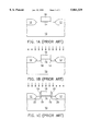
- FIGS. 1A through 1C are schematic sectional diagrams used to depict the steps involved in a conventional MOS transistor fabrication method.
- FIGS. 2A through 2C are schematic sectional diagrams used to depict the steps involved in a process according to the present invention for fabricating a MOS transistor.
- FIGS. 2A through 2C The new method of the invention for fabricating a MOS transistor will be described in the following with reference to FIGS. 2A through 2C. Elements in these figures that are identical in structure and purpose to those illustrated in FIGS. 1A through 1C will be labeled here with the same reference numerals.
- a semiconductor substrate such as a silicon substrate 10
- the silicon substrate 10 is then subjected to local oxidation of silicon (LOCOS) so as to form at least a pair of field oxide layers 12 thereon, which defines an active region on the silicon substrate 10.
- LOCOS local oxidation of silicon
- a gate dielectric layer 14 and a polysilicon gate layer 16 are successively formed over the active region, which two layers in combination form a gate (14, 16) for the MOS transistor.
- the method of the invention includes a featured process to form a thin dielectric layer over the gate dielectric layer and the source/drain regions, which helps to enhance the strength of the sidewall spacer on the gate.
- a featured process to form a thin dielectric layer over the gate dielectric layer and the source/drain regions, which helps to enhance the strength of the sidewall spacer on the gate.
- one way to perform the foregoing process is first to treat the wafer with a plasma of nitrogen so as to allow the polysilicon gate layer 16 and the surface of the silicon substrate 10 to contain nitrogen molecules.
- the gas for forming the plasma can be selected from the group consisting of nitrogen, nitrogen oxide, a mixture of nitrogen/oxygen, and ammonia.
- the plasma is applied to the wafer with an energy of 150 W and a flow rate of 100 sccm.
- an impurity semiconductor of a different type from that of the silicon substrate 10 is doped into the regions on both sides of the gate (14, 16) on the silicon substrate 10 so as to form a pair of LDD regions 18.
- a silicon dioxide layer is formed over the wafer and then etched back to remove part of the silicon dioxide layer.
- the remaining part of the silicon dioxide layer serves as a spacer 19 on the sidewall of the gate (14, 16).
- the nitrogen molecules in the polysilicon gate layer 16 and the surface of the silicon substrate 10 can react with the silicon in the same to form a thin layer of silicon nitride 17 which is the desired thin dielectric layer that covers the surfaces of the LDD regions 18 and the gate (14, 16).
- the LDD regions 18 are formed also by doping an impurity semiconductor of a different type from that of the silicon substrate 10 into those regions on both sides of the gate (14, 16) on the silicon substrate 10. Thereafter, the wafer is treated with a plasma of nitrogen, allowing the polysilicon gate layer 16 and the surface of the silicon substrate 10 to contain nitrogen molecules.
- the gas for forming the plasma is selected from the group consisting of nitrogen, nitrogen oxide, a mixture of nitrogen/oxygen, and ammonia.
- the plasma is applied to the wafer with an energy of 150 W and a flow rate of 100 sccm.
- a silicon dioxide layer is formed over the wafer and then etched back to remove part of the silicon dioxide layer.
- the remaining part of the silicon dioxide layer then serves as a spacer 19 on the sidewall of the gate (14, 16).
- the nitrogen molecules in the polysilicon gate layer 16 and the surface of the silicon substrate 10 can react with the silicon in the same to form a thin layer of silicon nitride 17 which is the desired thin dielectric layer that covers the surfaces of the LDD regions 18 and the gate (14, 16).
- the silicon dioxide spacer 19 on the sidewall of the gate (14, 16) is used as a mask to conduct an ion implantation process on the wafer so as to dope an impurity semiconductor with a high concentration into the LDD regions 18.
- the wafer is being heated so as to drive in the impurities in the LDD regions 18 to form a pair of source/drain regions 20 in the wafer.
- the impurity semiconductor is also doped into the polysilicon gate layer 16 so as to increase the conductivity thereof.
- a thin layer of silicon nitride covering the LDD regions and the gate can be formed in the wafer.
- This thin layer of silicon nitride acts as a barrier which prevents hot carriers from crossing the gate dielectric layer. As a result, the level of degradation to the MOS transistor due to hot carriers crossing the gate dielectric layer can be minimized.
Abstract
A method of fabricating a metal-oxide semiconductor (MOS) transistor is provided. This method is devised particularly to reduce the level of degradation to the MOS transistor caused by hot carriers. In the fabrication process, a plasma treatment is applied to the wafer to as to cause the forming of a thin layer of silicon nitride on the wafer which covers the gate and the lightly-doped diffusion (LDD) regions on the source/drain regions of the MOS transistor. This thin layer of silicon nitride acts as a barrier which prevents hot carriers from crossing the gate dielectric layer, such that the degradation of the MOS transistor due to hot carriers crossing the gate dielectric layer can be greatly minimized.
Description
1. Field of the Invention
This invention relates to semiconductor integrated circuit (IC) devices, and more particularly, to a method of fabricating a metal-oxide semiconductor (MOS) transistor with reduced level of degradation caused by hot carriers.
2. Description of Related Art
In designing MOS transistors, if the channel between the source/drain regions is reduced in size, the depletion regions in the source/drain regions will be overlapped with the channel, which effectively further reduces the size of the channel. In an enhancement mode MOS transistor, for example, if the bias applied thereto is fixed, the foregoing effect will cause the transversal electric field across the channel to be increased. As a consequence of this, the electrons in the channel will gain energy from the increased electric field. Therefore, the electrons near the junction between the channel and the drain region will be higher in energy than the electrons elsewhere that are in thermal equilibrium. These electrons are thus customarily referred to as "hot electrons". In proton-type MOS transistors, the energized protons are called "hot protons". Generically, these two kinds of carriers are both referred to as "hot carriers".
Since the hot carriers near the drain region gain an energy higher than the energy gap in the MOS transistor, the covalent electrons near the drain regions will be hit by these hot carriers and thereby raise in energy level to the conduction band. As a result, more electron-hole pairs will be produced. In conclusion, if the channel in the MOS transistor is shortened, the number of carriers in the channel near the drain region will be increased. This phenomenon is customarily referred to as "carrier multiplication".
These electrons that are additionally produced due to carrier multiplication will be attracted to the drain region, thus increasing the current in the drain region. In addition, part of these electrons can penetrate into the gate dielectric layer, thus causing the generation of more holes.
One part of these holes will flow to the substrate, thus causing a current flow in the substrate; and the other part of the same will be captured by the source region, thus causing an enhancement to the NPN junction that will cause the generation of more hot electrons. This increased level of carrier multiplication will cause the adverse effect of electrical breakdown in the MOS transistor, which means a degradation to the performance and characteristics of the MOS transistor.
One solution to reduce the level of carrier multiplication is to form a lightly doped diffusion (LDD) region in the source/drain regions near the channel, which is doped with a less concentration of impurities than the source/drain regions so as to reduce the intensity of the electric field across the channel. A conventional method for forming an LDD region in a MOS transistor is described in the following with reference to FIGS. 1A through 1C.
Referring first to FIG. 1A, in the foremost step, a semiconductor substrate, such as a silicon substrate 10, is prepared. The silicon substrate 10 is then subjected to local oxidation of silicon (LOCOS) so as to form at least a pair of field oxide layers 12 thereon, which defines an active region on the silicon substrate 10. Thereafter, a gate dielectric layer 14 and a polysilicon gate layer 16 are successively formed over the active region, which two layers in combination form a gate (14, 16) for the MOS transistor.
Referring further to FIG. 1B, in the subsequent step, a pair of LDD regions 18 is formed on the silicon substrate 10 by diffusing an impurity semiconductor with a low concentration into the regions on either side of the gate (14, 16).
Referring finally to FIG. 1C, in the subsequent step, a layer of a dielectric material, such as silicon dioxide, is formed on the sidewall of the gate (14, 16), which serves as a spacer 19 for the gate (14, 16). Thereafter, a pair of source/drain regions 20 are formed on the silicon substrate 10 by doping the same type of impurity semiconductor with a high concentration (i.e., the same impurity semiconductor that is used earlier to form the LDD regions 18 but here is applied with a higher concentration) into the LDD regions 18. At the same time during this process, the polysilicon gate layer 16 is also doped, such that the conductivity thereof is increased.
One major drawback to the foregoing method, however, is that the gate dielectric layer 14 could be easily get damaged during the process of doping the impurity semiconductor into the wafer to form the heavily doped regions that serve as the source/drain regions. Moreover, although the provision of the LDD regions in the source/drain regions can reduce the hot carrier effect, there are still a small number of hot carriers that will be accelerated by the electric field across the channel, which causes a high current in the channel that will then cause an electrical breakdown in the MOS transistor. Some of these hot carriers will even cross the gate dielectric layer 14 to the polysilicon gate layer 16 and thereby be trapped in the gate dielectric layer 14. The trapped carriers will cause a change in the amount of electric charges in the gate dielectric layer 14, thus altering the threshold voltage (Vt) of the MOS transistor. The characteristics and performance of the MOS transistor thus could be degraded.
It is therefore a primary objective of the present invention to provide a MOS transistor fabrication method which can reduce the level of degradation to the MOS transistor caused by hot carriers.
In accordance with the foregoing and other objectives of the present invention, a new and improved method for fabricating MOS transistors is provided. The method of the invention can be performed in two ways.
The first way to perform the method includes: a first step of preparing a semiconductor wafer of a first type; a second step of forming a gate and a field oxide layer on the wafer, the gate including a polysilicon electrode and a dielectric layer; a third step of conducting a plasma treatment on the wafer with a plasma of nitrogen; a fourth step of conducting a first ion implantation process on the gate and selected areas on both sides of the gate with an impurity semiconductor of a second type so as to form a pair of LDD regions on both sides of the gate and a thin layer of silicon nitride which covers the LDD regions and the gate; a fifth step of forming a silicon dioxide spacer on the sidewall of the gate; and a final sixth step of using the silicon dioxide spacer as a mask to conduct a second ion implantation process on the wafer with an impurity semiconductor of the second type so as to form a pair of heavily doped source/drain regions in the wafer.
The second way to perform the method is substantially the same as the foregoing process except that the fourth step in the foregoing process is performed prior to the third step; that is, the plasma treatment is performed after the step of forming the LDD regions.
By either way, a thin layer of silicon nitride covering the LDD regions and the gate can be formed in the wafer. This thin layer of silicon nitride acts a barrier which prevents hot carriers from crossing the gate dielectric layer, such that degradation of the MOS transistor due to hot carriers crossing the gate dielectric layer can be minimized.
The invention can be more fully understood by reading the following detailed description of the preferred embodiments, with reference made to the accompanying drawings, wherein:
FIGS. 1A through 1C are schematic sectional diagrams used to depict the steps involved in a conventional MOS transistor fabrication method; and
FIGS. 2A through 2C are schematic sectional diagrams used to depict the steps involved in a process according to the present invention for fabricating a MOS transistor.
The new method of the invention for fabricating a MOS transistor will be described in the following with reference to FIGS. 2A through 2C. Elements in these figures that are identical in structure and purpose to those illustrated in FIGS. 1A through 1C will be labeled here with the same reference numerals.
Referring first to FIG. 2A, the foremost step is the same as depicted with reference to FIG. 1A, in which a semiconductor substrate, such as a silicon substrate 10, is prepared. The silicon substrate 10 is then subjected to local oxidation of silicon (LOCOS) so as to form at least a pair of field oxide layers 12 thereon, which defines an active region on the silicon substrate 10. Thereafter, a gate dielectric layer 14 and a polysilicon gate layer 16 are successively formed over the active region, which two layers in combination form a gate (14, 16) for the MOS transistor.
To suppress the effect caused by hot carriers crossing the gate dielectric layer, the method of the invention includes a featured process to form a thin dielectric layer over the gate dielectric layer and the source/drain regions, which helps to enhance the strength of the sidewall spacer on the gate. There are two ways to form such a thin dielectric layer, which will be respectively described in the following with reference to FIG. 2B.
Referring to FIG. 2B, one way to perform the foregoing process is first to treat the wafer with a plasma of nitrogen so as to allow the polysilicon gate layer 16 and the surface of the silicon substrate 10 to contain nitrogen molecules. The gas for forming the plasma can be selected from the group consisting of nitrogen, nitrogen oxide, a mixture of nitrogen/oxygen, and ammonia. The plasma is applied to the wafer with an energy of 150 W and a flow rate of 100 sccm. Following this, an impurity semiconductor of a different type from that of the silicon substrate 10 is doped into the regions on both sides of the gate (14, 16) on the silicon substrate 10 so as to form a pair of LDD regions 18. Thereafter, a silicon dioxide layer is formed over the wafer and then etched back to remove part of the silicon dioxide layer. The remaining part of the silicon dioxide layer serves as a spacer 19 on the sidewall of the gate (14, 16). The nitrogen molecules in the polysilicon gate layer 16 and the surface of the silicon substrate 10 can react with the silicon in the same to form a thin layer of silicon nitride 17 which is the desired thin dielectric layer that covers the surfaces of the LDD regions 18 and the gate (14, 16).
Another way to perform the foregoing process is to firstly form the LDD regions 18 and then conduct the plasma treatment in the subsequent step. The LDD regions 18 are formed also by doping an impurity semiconductor of a different type from that of the silicon substrate 10 into those regions on both sides of the gate (14, 16) on the silicon substrate 10. Thereafter, the wafer is treated with a plasma of nitrogen, allowing the polysilicon gate layer 16 and the surface of the silicon substrate 10 to contain nitrogen molecules. The gas for forming the plasma is selected from the group consisting of nitrogen, nitrogen oxide, a mixture of nitrogen/oxygen, and ammonia. The plasma is applied to the wafer with an energy of 150 W and a flow rate of 100 sccm. Subsequently, a silicon dioxide layer is formed over the wafer and then etched back to remove part of the silicon dioxide layer. The remaining part of the silicon dioxide layer then serves as a spacer 19 on the sidewall of the gate (14, 16). The nitrogen molecules in the polysilicon gate layer 16 and the surface of the silicon substrate 10 can react with the silicon in the same to form a thin layer of silicon nitride 17 which is the desired thin dielectric layer that covers the surfaces of the LDD regions 18 and the gate (14, 16).
Referring finally to FIG. 2C, in the subsequent step, the silicon dioxide spacer 19 on the sidewall of the gate (14, 16) is used as a mask to conduct an ion implantation process on the wafer so as to dope an impurity semiconductor with a high concentration into the LDD regions 18. At the same time during this process, the wafer is being heated so as to drive in the impurities in the LDD regions 18 to form a pair of source/drain regions 20 in the wafer. By this process, the impurity semiconductor is also doped into the polysilicon gate layer 16 so as to increase the conductivity thereof. To complete the fabrication of the MOS transistor, all the following steps involve conventional techniques so that description thereof will not be detailed.
By either way, a thin layer of silicon nitride covering the LDD regions and the gate can be formed in the wafer. This thin layer of silicon nitride acts as a barrier which prevents hot carriers from crossing the gate dielectric layer. As a result, the level of degradation to the MOS transistor due to hot carriers crossing the gate dielectric layer can be minimized.
The invention has been described using exemplary preferred embodiments. However, it is to be understood that the scope of the invention is not limited to the disclosed embodiments. To the contrary, it is intended to cover various modifications and similar arrangements. The scope of the claims, therefore, should be accorded the broadest interpretation so as to encompass all such modifications and similar arrangements.
Claims (8)
1. A method for fabricating a MOS transistor, comprising the steps of:
(1) preparing a semiconductor wafer of a first type;
(2) forming a gate and a field oxide layer on the wafer, the gate including a polysilicon electrode and a dielectric layer;
(3) conducting a plasma treatment on the wafer with a plasma of nitrogen;
(4) conducting a first ion implantation process on the gate and selected areas on both sides of the gate with an impurity semiconductor of a second type so as to form a pair of LDD regions on both sides of the gate and a thin layer of silicon nitride which covers the LDD regions and the gate;
(5) forming a spacer of silicon dioxide on the sidewall of the gate, the silicon nitride remaining over the LLD regions and the gate, and forming; and
(6) using the spacer as a mask to conduct a second ion implantation process on the wafer with an impurity semiconductor of the second type so as to form a pair of heavily doped source/drain regions in the wafer.
2. The method of claim 1, wherein the plasma is formed by using a gas selected from the group consisting of N2, nitrogen oxide, a mixture of nitrogen/oxygen, and ammonia.
3. The method of claim 2, wherein the plasma is applied to the wafer with an energy of 150 W and a flow rate of 100 sccm.
4. A method for fabricating a MOS transistor, comprising the steps of:
(1) preparing a semiconductor wafer of a first type;
(2) forming a gate and a field oxide layer on the wafer, the gate including a polysilicon electrode and a dielectric layer;
(3) conducting a first ion implantation process on the gate and selected areas on both sides of the gate with an impurity semiconductor of a second type so as to lightly dope the gate and form a pair of LDD regions on both sides of the gate;
(4) conducting a plasma treatment on the wafer with a plasma of nitrogen, thereby allowing the forming of a thin layer of silicon nitride which covers the LDD regions and the gate;
(5) forming a spacer of silicon dioxide on the sidewall of the gate, the silicon nitride remaining over the LLD regions and the gate; and
(6) using the spacer as a mask to conduct a second ion implantation process on the wafer with an impurity semiconductor of the second type so as to form a pair of heavily doped source/drain regions in the wafer.
5. The method of claim 4, wherein the plasma is formed by using a gas selected from the group consisting of N2, nitrogen oxide, a mixture of nitrogen/oxygen, and ammonia.
6. The method of claim 5, wherein the plasma is applied to the wafer with an energy of 150 W and a flow rate of 100 sccm.
7. A method of making a MOS transistor, comprising:
forming a gate on a substrate;
forming source/drain regions in the substrate, and on opposite sides of the gate; and
forming a dielectric layer over the gate and locatable over the source/drain regions, wherein said forming a gate includes forming a gate dielectric layer on the substrate, and forming a polysilicon gate layer on the gate dielectric layer, Wherein said forming a dielectric layer includes:
infusing the polysilicon gate layer and a surface of the substrate with a plasma of nitrogen molecules;
forming silicon dioxide spacers on sidewalls of the gate; and reacting the nitrogen molecules with silicon in the silicon dioxide spacers and the polysilicon gate layer to form the dielectric layer.
8. The method recited in claim 7, wherein the dielectric layer comprises silicon nitride.
Applications Claiming Priority (2)
| Application Number | Priority Date | Filing Date | Title |
|---|---|---|---|
| TW85112827 | 1996-10-19 | ||
| TW085112827A TW317012B (en) | 1996-10-19 | 1996-10-19 | Process of improving semiconductor device degradation caused by hot carrier |
Publications (1)
| Publication Number | Publication Date |
|---|---|
| US5861329A true US5861329A (en) | 1999-01-19 |
Family
ID=21625505
Family Applications (1)
| Application Number | Title | Priority Date | Filing Date |
|---|---|---|---|
| US08/764,254 Expired - Lifetime US5861329A (en) | 1996-10-19 | 1996-12-12 | Method of fabricating metal-oxide semiconductor (MOS) transistors with reduced level of degradation caused by hot carriers |
Country Status (2)
| Country | Link |
|---|---|
| US (1) | US5861329A (en) |
| TW (1) | TW317012B (en) |
Cited By (7)
| Publication number | Priority date | Publication date | Assignee | Title |
|---|---|---|---|---|
| US6162717A (en) * | 1998-06-19 | 2000-12-19 | Promos Technologies, Inc | Method of manufacturing MOS gate utilizing a nitridation reaction |
| KR20010059854A (en) * | 1999-12-30 | 2001-07-06 | 박종섭 | Semiconductor device and method for forming the same |
| US6383880B1 (en) * | 2000-10-05 | 2002-05-07 | Advanced Micro Devices, Inc. | NH3/N2-plasma treatment for reduced nickel silicide bridging |
| US6486064B1 (en) * | 2000-09-26 | 2002-11-26 | Lsi Logic Corporation | Shallow junction formation |
| US7176094B2 (en) | 2002-03-06 | 2007-02-13 | Chartered Semiconductor Manufacturing Ltd. | Ultra-thin gate oxide through post decoupled plasma nitridation anneal |
| US7928020B2 (en) | 2007-09-27 | 2011-04-19 | Chartered Semiconductor Manufacturing Ltd. | Method of fabricating a nitrogenated silicon oxide layer and MOS device having same |
| US9780178B2 (en) * | 2015-06-05 | 2017-10-03 | Globalfoundries Inc. | Methods of forming a gate contact above an active region of a semiconductor device |
Citations (8)
| Publication number | Priority date | Publication date | Assignee | Title |
|---|---|---|---|---|
| US4277320A (en) * | 1979-10-01 | 1981-07-07 | Rockwell International Corporation | Process for direct thermal nitridation of silicon semiconductor devices |
| US4298629A (en) * | 1979-03-09 | 1981-11-03 | Fujitsu Limited | Method for forming a nitride insulating film on a silicon semiconductor substrate surface by direct nitridation |
| US4331710A (en) * | 1980-09-08 | 1982-05-25 | Fujitsu Limited | Method of forming an insulation film on semiconductor device surface |
| US4960723A (en) * | 1989-03-30 | 1990-10-02 | Motorola, Inc. | Process for making a self aligned vertical field effect transistor having an improved source contact |
| US5332697A (en) * | 1989-05-31 | 1994-07-26 | Smith Rosemary L | Formation of silicon nitride by nitridation of porous silicon |
| US5532176A (en) * | 1992-04-17 | 1996-07-02 | Nippondenso Co., Ltd. | Process for fabricating a complementary MIS transistor |
| US5567638A (en) * | 1995-06-14 | 1996-10-22 | National Science Council | Method for suppressing boron penetration in PMOS with nitridized polysilicon gate |
| US5674788A (en) * | 1995-06-06 | 1997-10-07 | Advanced Micro Devices, Inc. | Method of forming high pressure silicon oxynitride gate dielectrics |
-
1996
- 1996-10-19 TW TW085112827A patent/TW317012B/en not_active IP Right Cessation
- 1996-12-12 US US08/764,254 patent/US5861329A/en not_active Expired - Lifetime
Patent Citations (8)
| Publication number | Priority date | Publication date | Assignee | Title |
|---|---|---|---|---|
| US4298629A (en) * | 1979-03-09 | 1981-11-03 | Fujitsu Limited | Method for forming a nitride insulating film on a silicon semiconductor substrate surface by direct nitridation |
| US4277320A (en) * | 1979-10-01 | 1981-07-07 | Rockwell International Corporation | Process for direct thermal nitridation of silicon semiconductor devices |
| US4331710A (en) * | 1980-09-08 | 1982-05-25 | Fujitsu Limited | Method of forming an insulation film on semiconductor device surface |
| US4960723A (en) * | 1989-03-30 | 1990-10-02 | Motorola, Inc. | Process for making a self aligned vertical field effect transistor having an improved source contact |
| US5332697A (en) * | 1989-05-31 | 1994-07-26 | Smith Rosemary L | Formation of silicon nitride by nitridation of porous silicon |
| US5532176A (en) * | 1992-04-17 | 1996-07-02 | Nippondenso Co., Ltd. | Process for fabricating a complementary MIS transistor |
| US5674788A (en) * | 1995-06-06 | 1997-10-07 | Advanced Micro Devices, Inc. | Method of forming high pressure silicon oxynitride gate dielectrics |
| US5567638A (en) * | 1995-06-14 | 1996-10-22 | National Science Council | Method for suppressing boron penetration in PMOS with nitridized polysilicon gate |
Cited By (7)
| Publication number | Priority date | Publication date | Assignee | Title |
|---|---|---|---|---|
| US6162717A (en) * | 1998-06-19 | 2000-12-19 | Promos Technologies, Inc | Method of manufacturing MOS gate utilizing a nitridation reaction |
| KR20010059854A (en) * | 1999-12-30 | 2001-07-06 | 박종섭 | Semiconductor device and method for forming the same |
| US6486064B1 (en) * | 2000-09-26 | 2002-11-26 | Lsi Logic Corporation | Shallow junction formation |
| US6383880B1 (en) * | 2000-10-05 | 2002-05-07 | Advanced Micro Devices, Inc. | NH3/N2-plasma treatment for reduced nickel silicide bridging |
| US7176094B2 (en) | 2002-03-06 | 2007-02-13 | Chartered Semiconductor Manufacturing Ltd. | Ultra-thin gate oxide through post decoupled plasma nitridation anneal |
| US7928020B2 (en) | 2007-09-27 | 2011-04-19 | Chartered Semiconductor Manufacturing Ltd. | Method of fabricating a nitrogenated silicon oxide layer and MOS device having same |
| US9780178B2 (en) * | 2015-06-05 | 2017-10-03 | Globalfoundries Inc. | Methods of forming a gate contact above an active region of a semiconductor device |
Also Published As
| Publication number | Publication date |
|---|---|
| TW317012B (en) | 1997-10-01 |
Similar Documents
| Publication | Publication Date | Title |
|---|---|---|
| US6426279B1 (en) | Epitaxial delta doping for retrograde channel profile | |
| KR100302187B1 (en) | Method for fabricating semiconductor device | |
| JP2002124671A (en) | Semiconductor device and its manufacturing method | |
| KR19980050121A (en) | Transistor and manufacturing method | |
| US5861329A (en) | Method of fabricating metal-oxide semiconductor (MOS) transistors with reduced level of degradation caused by hot carriers | |
| KR100574172B1 (en) | Method for fabricating semiconductor device | |
| KR100285995B1 (en) | Manufacturing method of MIS transistor | |
| US7235450B2 (en) | Methods for fabricating semiconductor devices | |
| EP0481559A2 (en) | A method of fabricating a field-effect transistor | |
| US20020155686A1 (en) | Fabrication method for suppressing a hot carrier effect and leakage currents of I/O devices | |
| JP2623902B2 (en) | Semiconductor device and manufacturing method thereof | |
| JP2757491B2 (en) | Method for manufacturing semiconductor device | |
| US6060767A (en) | Semiconductor device having fluorine bearing sidewall spacers and method of manufacture thereof | |
| KR100549941B1 (en) | gate electrode structure for semiconductor device | |
| KR100252747B1 (en) | Flash memory device and manufacturing method thereof | |
| JPH05267338A (en) | Manufacture of semiconductor device | |
| JP2591518B2 (en) | Semiconductor device | |
| KR0156157B1 (en) | Method of fabricating semiconductor device | |
| JPH0348428A (en) | Semiconductor device | |
| KR100588787B1 (en) | Fabricating method of semiconductor device | |
| KR100588784B1 (en) | Fabricating method of semiconductor device | |
| JPH0621441A (en) | Mos transistor | |
| KR100531105B1 (en) | Fabricating method of semiconductor device | |
| KR100546812B1 (en) | Fabricating method of semiconductor device | |
| US20020089021A1 (en) | Semiconductor device with an anti-doped region |
Legal Events
| Date | Code | Title | Description |
|---|---|---|---|
| AS | Assignment |
Owner name: UNITED MICROELECTRONICS CORPORATION, TAIWAN Free format text: ASSIGNMENT OF ASSIGNORS INTEREST;ASSIGNORS:YEH, WEN-KUAN;CHEN, COMING;TSAI, MENG JIN;AND OTHERS;REEL/FRAME:008393/0329;SIGNING DATES FROM 19961114 TO 19961122 |
|
| STCF | Information on status: patent grant |
Free format text: PATENTED CASE |
|
| FPAY | Fee payment |
Year of fee payment: 4 |
|
| FPAY | Fee payment |
Year of fee payment: 8 |
|
| FPAY | Fee payment |
Year of fee payment: 12 |