US5874326A - Method for fabricating thin film transistor - Google Patents
Method for fabricating thin film transistor Download PDFInfo
- Publication number
- US5874326A US5874326A US08/899,207 US89920797A US5874326A US 5874326 A US5874326 A US 5874326A US 89920797 A US89920797 A US 89920797A US 5874326 A US5874326 A US 5874326A
- Authority
- US
- United States
- Prior art keywords
- layer
- insulating layer
- thin film
- film transistor
- fabricating
- Prior art date
- Legal status (The legal status is an assumption and is not a legal conclusion. Google has not performed a legal analysis and makes no representation as to the accuracy of the status listed.)
- Expired - Lifetime
Links
- 238000000034 method Methods 0.000 title claims abstract description 44
- 239000010409 thin film Substances 0.000 title claims abstract description 28
- 239000004065 semiconductor Substances 0.000 claims abstract description 59
- 238000005530 etching Methods 0.000 claims abstract description 20
- 239000002184 metal Substances 0.000 claims abstract description 17
- 229910052751 metal Inorganic materials 0.000 claims abstract description 17
- 239000010410 layer Substances 0.000 claims description 224
- 239000000758 substrate Substances 0.000 claims description 14
- 239000012535 impurity Substances 0.000 claims description 9
- 239000011347 resin Substances 0.000 claims description 9
- 229920005989 resin Polymers 0.000 claims description 9
- 229910004205 SiNX Inorganic materials 0.000 claims description 5
- VYPSYNLAJGMNEJ-UHFFFAOYSA-N Silicium dioxide Chemical compound O=[Si]=O VYPSYNLAJGMNEJ-UHFFFAOYSA-N 0.000 claims description 5
- 229910052814 silicon oxide Inorganic materials 0.000 claims description 5
- 238000000151 deposition Methods 0.000 claims description 3
- 239000012044 organic layer Substances 0.000 claims description 3
- 229910021417 amorphous silicon Inorganic materials 0.000 description 37
- 239000004973 liquid crystal related substance Substances 0.000 description 8
- 238000009413 insulation Methods 0.000 description 3
- 238000002161 passivation Methods 0.000 description 3
- 229910000838 Al alloy Inorganic materials 0.000 description 2
- 239000011521 glass Substances 0.000 description 2
- 150000002500 ions Chemical class 0.000 description 2
- 238000005229 chemical vapour deposition Methods 0.000 description 1
- 238000007796 conventional method Methods 0.000 description 1
- 238000004020 luminiscence type Methods 0.000 description 1
- 238000004519 manufacturing process Methods 0.000 description 1
- 239000000463 material Substances 0.000 description 1
- 239000011159 matrix material Substances 0.000 description 1
- 238000012986 modification Methods 0.000 description 1
- 230000004048 modification Effects 0.000 description 1
- 238000001259 photo etching Methods 0.000 description 1
- 238000005268 plasma chemical vapour deposition Methods 0.000 description 1
Images

Classifications
-
- H—ELECTRICITY
- H01—ELECTRIC ELEMENTS
- H01L—SEMICONDUCTOR DEVICES NOT COVERED BY CLASS H10
- H01L21/00—Processes or apparatus adapted for the manufacture or treatment of semiconductor or solid state devices or of parts thereof
- H01L21/02—Manufacture or treatment of semiconductor devices or of parts thereof
- H01L21/04—Manufacture or treatment of semiconductor devices or of parts thereof the devices having at least one potential-jump barrier or surface barrier, e.g. PN junction, depletion layer or carrier concentration layer
- H01L21/18—Manufacture or treatment of semiconductor devices or of parts thereof the devices having at least one potential-jump barrier or surface barrier, e.g. PN junction, depletion layer or carrier concentration layer the devices having semiconductor bodies comprising elements of Group IV of the Periodic System or AIIIBV compounds with or without impurities, e.g. doping materials
-
- H—ELECTRICITY
- H01—ELECTRIC ELEMENTS
- H01L—SEMICONDUCTOR DEVICES NOT COVERED BY CLASS H10
- H01L27/00—Devices consisting of a plurality of semiconductor or other solid-state components formed in or on a common substrate
- H01L27/02—Devices consisting of a plurality of semiconductor or other solid-state components formed in or on a common substrate including semiconductor components specially adapted for rectifying, oscillating, amplifying or switching and having at least one potential-jump barrier or surface barrier; including integrated passive circuit elements with at least one potential-jump barrier or surface barrier
- H01L27/12—Devices consisting of a plurality of semiconductor or other solid-state components formed in or on a common substrate including semiconductor components specially adapted for rectifying, oscillating, amplifying or switching and having at least one potential-jump barrier or surface barrier; including integrated passive circuit elements with at least one potential-jump barrier or surface barrier the substrate being other than a semiconductor body, e.g. an insulating body
- H01L27/1214—Devices consisting of a plurality of semiconductor or other solid-state components formed in or on a common substrate including semiconductor components specially adapted for rectifying, oscillating, amplifying or switching and having at least one potential-jump barrier or surface barrier; including integrated passive circuit elements with at least one potential-jump barrier or surface barrier the substrate being other than a semiconductor body, e.g. an insulating body comprising a plurality of TFTs formed on a non-semiconducting substrate, e.g. driving circuits for AMLCDs
- H01L27/1259—Multistep manufacturing methods
- H01L27/1288—Multistep manufacturing methods employing particular masking sequences or specially adapted masks, e.g. half-tone mask
-
- H—ELECTRICITY
- H01—ELECTRIC ELEMENTS
- H01L—SEMICONDUCTOR DEVICES NOT COVERED BY CLASS H10
- H01L27/00—Devices consisting of a plurality of semiconductor or other solid-state components formed in or on a common substrate
- H01L27/02—Devices consisting of a plurality of semiconductor or other solid-state components formed in or on a common substrate including semiconductor components specially adapted for rectifying, oscillating, amplifying or switching and having at least one potential-jump barrier or surface barrier; including integrated passive circuit elements with at least one potential-jump barrier or surface barrier
- H01L27/12—Devices consisting of a plurality of semiconductor or other solid-state components formed in or on a common substrate including semiconductor components specially adapted for rectifying, oscillating, amplifying or switching and having at least one potential-jump barrier or surface barrier; including integrated passive circuit elements with at least one potential-jump barrier or surface barrier the substrate being other than a semiconductor body, e.g. an insulating body
- H01L27/1214—Devices consisting of a plurality of semiconductor or other solid-state components formed in or on a common substrate including semiconductor components specially adapted for rectifying, oscillating, amplifying or switching and having at least one potential-jump barrier or surface barrier; including integrated passive circuit elements with at least one potential-jump barrier or surface barrier the substrate being other than a semiconductor body, e.g. an insulating body comprising a plurality of TFTs formed on a non-semiconducting substrate, e.g. driving circuits for AMLCDs
- H01L27/1248—Devices consisting of a plurality of semiconductor or other solid-state components formed in or on a common substrate including semiconductor components specially adapted for rectifying, oscillating, amplifying or switching and having at least one potential-jump barrier or surface barrier; including integrated passive circuit elements with at least one potential-jump barrier or surface barrier the substrate being other than a semiconductor body, e.g. an insulating body comprising a plurality of TFTs formed on a non-semiconducting substrate, e.g. driving circuits for AMLCDs with a particular composition or shape of the interlayer dielectric specially adapted to the circuit arrangement
-
- H—ELECTRICITY
- H01—ELECTRIC ELEMENTS
- H01L—SEMICONDUCTOR DEVICES NOT COVERED BY CLASS H10
- H01L29/00—Semiconductor devices adapted for rectifying, amplifying, oscillating or switching, or capacitors or resistors with at least one potential-jump barrier or surface barrier, e.g. PN junction depletion layer or carrier concentration layer; Details of semiconductor bodies or of electrodes thereof ; Multistep manufacturing processes therefor
- H01L29/66—Types of semiconductor device ; Multistep manufacturing processes therefor
- H01L29/66007—Multistep manufacturing processes
- H01L29/66075—Multistep manufacturing processes of devices having semiconductor bodies comprising group 14 or group 13/15 materials
- H01L29/66227—Multistep manufacturing processes of devices having semiconductor bodies comprising group 14 or group 13/15 materials the devices being controllable only by the electric current supplied or the electric potential applied, to an electrode which does not carry the current to be rectified, amplified or switched, e.g. three-terminal devices
- H01L29/66409—Unipolar field-effect transistors
- H01L29/66477—Unipolar field-effect transistors with an insulated gate, i.e. MISFET
- H01L29/66742—Thin film unipolar transistors
- H01L29/6675—Amorphous silicon or polysilicon transistors
- H01L29/66765—Lateral single gate single channel transistors with inverted structure, i.e. the channel layer is formed after the gate
-
- H—ELECTRICITY
- H01—ELECTRIC ELEMENTS
- H01L—SEMICONDUCTOR DEVICES NOT COVERED BY CLASS H10
- H01L29/00—Semiconductor devices adapted for rectifying, amplifying, oscillating or switching, or capacitors or resistors with at least one potential-jump barrier or surface barrier, e.g. PN junction depletion layer or carrier concentration layer; Details of semiconductor bodies or of electrodes thereof ; Multistep manufacturing processes therefor
- H01L29/66—Types of semiconductor device ; Multistep manufacturing processes therefor
- H01L29/68—Types of semiconductor device ; Multistep manufacturing processes therefor controllable by only the electric current supplied, or only the electric potential applied, to an electrode which does not carry the current to be rectified, amplified or switched
- H01L29/76—Unipolar devices, e.g. field effect transistors
- H01L29/772—Field effect transistors
- H01L29/78—Field effect transistors with field effect produced by an insulated gate
- H01L29/786—Thin film transistors, i.e. transistors with a channel being at least partly a thin film
- H01L29/78651—Silicon transistors
- H01L29/7866—Non-monocrystalline silicon transistors
- H01L29/78663—Amorphous silicon transistors
- H01L29/78669—Amorphous silicon transistors with inverted-type structure, e.g. with bottom gate
Definitions
- the present invention relates to liquid crystal display devices, and more particularly to a simplified method for fabricating liquid crystal displays in which an organic or inorganic insulating layer can be applied as a passivation layer according to the thickness of a semiconductor layer or etching selection ratio of the etch stopper layer.
- the cathode ray tube(CRT) display device has a large screen area.
- the screen on which the luminescence material is coated must be separated from the electron gun a distance greater than that prescribed for the large screen area, a CRT display device has a large volume. Therefore, CRT devices cannot be used in a low power consumption portable television, small notebook computers or the like.
- LCD liquid crystal display
- PDP plasma display panel
- VFD vacuum florescent display
- ELD electrostatic display
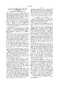
- FIG. 1 is a partial plan view of an AMLCD.
- This LCD is a TFT(thin film transistor) LCD.
- a plurality of pixels are formed in a matrix shape by a plurality of gate bus lines 1 and data bus lines 7 which extend in the horizontal and vertical directions. For explanatory purposes, only one pixel is described.
- pixel electrode 9 is formed and TFT 2 is formed at the intersection of gate bus line 1 and data bus line 7.
- a gate electrode 11 and source/drain electrode 17 of TFT 2 are connected to gate bus line 1 and data bus line 7, respectively.
- ES TFT etch stopper TFT
- BCE TFT back channel etched TFT
- the ES layer is formed over the semiconductor layer to prevent the channel region of the semiconductor layer from being etched when the semiconductor layer and the source/drain electrodes are etched.
- the BCE TFT since there is no insulating layer on the semiconductor layer, the process is simpler, although the semiconductor layer in the channel region is etched during the process.
- FIGS. 2a-2f illustrate various steps of the conventional process for fabricating a TFT with inverted stagger structure.
- metal is first deposited on to a transparent glass substrate 10 and etched to form a gate electrode 11.
- gate electrode 11 Over the substrate 10 and gate electrode 11, as shown in FIG. 2b, gate insulating layer 13, amorphous silicon(a-Si) layer 14a, and insulating layer 15a are successively deposited.
- the insulating layer 15a is etched to form and ES layer 15, as shown in FIG. 2c.
- n + a-Si layer 16a and metal layer 17a are deposited after a-Si layer 14a is etched to form a semiconductor layer 14.
- the n + a-Si layer 16 and metal layer 17a are etched.
- a portion of ES layer 15 overlaps n + layer 16 and another portion is exposed.
- the passivation layer(not shown) is deposited on source/drain electrodes 17 and ES layer 15.
- a contact hole is formed in the passivation layer and the pixel electrode 9 covers pixel region to connect it to source/drain electrodes 17.
- ES layer 15 covers the channel region of semiconductor layer 14, the channel region is non affected during the etching of the a-Si 14a and the n + a-Si 16a layers.
- six masks are needed to fabricate the TFT of the LCD; that is, masks for forming the gate electrodes, ES layer, semiconductor layer, source/drain electrodes and n + layer, contact hole, and pixel electrode. The resulting process is complex and costly.
- An object of the present invention is to provide a method for fabricating a thin film transistor of a liquid crystal display device, in which the semiconductor layer and n + layer can be etched on a substrate with a single process.
- Another object of the present invention is to provide a method for fabricating a thin film transistor of the liquid crystal display device having single or double insulating layers.
- a method consistent with this invention includes the steps of a method for fabricating a thin film transistor comprising the steps of providing a substrate, forming a gate electrode on the substrate, depositing a gate insulating layer on the substrate and the gate electrode, forming a semiconductor layer on the gate insulating layer, forming a first insulating layer on a portion of the semiconductor layer, forming an impurity semiconductor layer on the first insulating layer and semiconductor, forming a metal layer on the impurity semiconductor layer, etching the metal layer, the impurity semiconductor layer, the first insulating layer, and the semiconductor layer with a single process so as to form an ohmic contact layer and source/drain electrodes, and forming at least one second insulating layer on the gate insulating layer and the source/drain electrodes.
- a device consistent with the present invention includes a thin film transistor formed by the method of providing a substrate, forming a gate electrode on the substrate, depositing a gate insulating layer on the substrate and the gate electrode, forming a semiconductor layer on the gate insulating layer, forming a first insulating layer on a portion of the semiconductor layer, forming an impurity semiconductor layer on the first insulating layer and the semiconductor, forming a metal layer on the impurity semiconductor layer, etching the metal layer, the impurity semiconductor layer, the first insulating layer, and the semiconductor layer with a single process so as to form an ohmic contact layer and source/drain electrodes, and forming a least one second insulating layer on the gate insulating layer and the source/drain electrodes.
- FIG. 1 is a partial plan view showing one pixel of a liquid crystal display device.
- FIGS. 2a-2f are views illustrating the conventional method of fabricating a thin film transistor of a liquid crystal display device.
- FIGS. 3a-3g are views illustrating the method of fabricating the thin film transistor of a liquid crystal display consistent with the present invention.
- FIG. 4 is an enlarged view of part A of FIG. 3e.
- FIGS. 5a and 5b are enlarged views of part B of FIG. 3e.
- FIGS. 6a and 6b are enlarged views of part C of FIG. 3f.
- a metal such as Mo, Cr, Al, or Al alloy
- a metal is deposited onto a transparent glass substrate 110 and then etched with a photoetching process to form a gate electrode 111.
- the gate insulation layer 113, a-Si layer 114a, and ES insulation layer 115a are formed on gate electrode 111 and substrate 110.
- gate insulation layer 113(of SiOx or SiNx) and a-Si layer 114a are successively formed by plasma chemical vapor deposition(CVD).
- insulating layer 115a is etched to form an ES layer 115.
- semiconductor layer 114a is doped with n + ions or n + a-Si is directly deposited by plasma CVD to form an n + a-Si layer 116a.
- Metal comprising Cr, Mo, Al, or Al alloy is deposited thereon to form a metal layer 117a on ES layer 115 and a-Si layer 114a.
- a-Si layer 114a is doped with n + ions, an n + a-Si layer 116a is formed only on a-Si layer 114a, not on ES layer 115.
- n + a-Si is directly deposited, n + a-Si layer 116a is formed on a-Si layer 114a and ES layer 115.
- Metal layer 117a, n + a-Si layer 116a, a-Si layer 114a and ES layer 115 are etched with a single process to form semiconductor layer 114, ohmic contact layer 116, and source/drain electrodes 117, as shown in FIG. 3e. That is, ES layer 115, n + a-Si layer 116a, and metal layer 117a are etched in part B, while a-Si layer 114a, n + a-Si layer 116a, and metal layer 117a are etched in part A, as shown in FIGS. 4 and 5a.
- a-Si layer 114a of part A and ES layer 115 of part B are etched after the etching process of n + a-Si layer 116a and metal layer 117a of parts A and B. If a-Si layer 114a is thinner than ES layer 115, ES layer 115 is etched as much as a-Si layer 114a. As a result, a portion of ES layer 115 remains in the channel region, as shown in FIG. 5a. If the a-Si layer is thicker than ES layer 115, ES layer 115 is etched and then a portion of the a-Si layer 114a in the channel region is also etched, as shown in FIG. 5b.
- ES layer 115 has an etching selection ratio lower than that of a-Si layer 114a, a portion of ES layer 115 remains in the channel region because of the difference of the etching speed. Further, if the etching selection ratio of the ES layer 115 is higher than that of a-Si layer 114a, a portion of semiconductor layer 114a in the channel region is etched.
- a single insulating layer or double insulating layers are formed on semiconductor layer 114 and source/drain electrodes 117. If a-Si layer 114a is thinner than ES layer 115 or if ES layer 115 has a lower etching selection ratio than a-Si layer 114a, ES layer 115 remains in the channel region of semiconductor layer 114. Thus, an organic layer 121 such as resin is used as an insulating layer, as shown in FIG. 6a. Further, if a-Si layer 114a is thicker than ES layer 115 or if ES layer 115 has a higher etching selection ratio than a-Si layer 114a, semiconductor layer 114 in the channel region is exposed.
- inorganic insulating layer 120 including SiNx and SiOx is formed on semiconductor layer 114 and source/drain electrodes 117 and organic insulating layer 121 such as resin is next formed thereon, as shown in FIG. 6b.
- FIG. 6b shows a TFT comprising two insulating layers, inorganic insulating layer 120 and organic insulating layer 121, a TFT comprising only one insulating layer, for example, organic insulating layer 121, is possible as shown in FIG. 6a.
- insulating layer 120 and 121 are patterned to form the contact hole over source/drain electrodes 117 and then a pixel electrode 125 is deposited on insulating layers 120 and 121 in the pixel region.
- a pixel electrode 125 is deposited on insulating layers 120 and 121 in the pixel region.
- the TFT shape varies. Specifically, when semiconductor layer 114 is thinner than ES layer 115 or the etching selection ratio of ES layer 115 is lower than that of semiconductor layer 114, the TFT is an ES TFT. Further, when semiconductor layer 114 is thicker than ES layer 115 or the etching selection ratio of ES layer 115 is higher than that of semiconductor layer 114, the TFT is a BCE TFT.
- ES TFT In an ES TFT, since ES layer 115 covers the channel region of semiconductor layer 114, organic insulating layer 121 including resin is formed on source/drain electrodes 117 and semiconductor layer 114. In a BCE TFT, because semiconductor layer 114 in the channel region is exposed, inorganic insulating layer 120 including SiNx and SiOx is formed and inorganic insulating layer 121 such as resin as resin are also formed thereon.
- the semiconductor layer, the ohmic contact layer, the source/drain electrodes, and the ES layer are etched with single process, there is need to provide five masks as follows: a mask for forming the gate electrode; a mask for forming the ES layer; a mask for forming the semiconductor layer, the n + a-Si layer, and the source/drain electrodes; a mask for forming contact hole; and a mask for forming pixel electrodes. Therefore, the process is simpler than the conventional process.
- the ES TFT or BCE TFT can be fabricated by controlling the thickness of the semiconductor layer or the etching-selection ratio of the ES layer, a TFT of the desired type can be fabricated.
Abstract
Description
Claims (17)
Applications Claiming Priority (2)
| Application Number | Priority Date | Filing Date | Title |
|---|---|---|---|
| KR1996-30828 | 1996-07-27 | ||
| KR19960030828A KR100196336B1 (en) | 1996-07-27 | 1996-07-27 | Method of manufacturing thin film transistor |
Publications (1)
| Publication Number | Publication Date |
|---|---|
| US5874326A true US5874326A (en) | 1999-02-23 |
Family
ID=19467782
Family Applications (1)
| Application Number | Title | Priority Date | Filing Date |
|---|---|---|---|
| US08/899,207 Expired - Lifetime US5874326A (en) | 1996-07-27 | 1997-07-23 | Method for fabricating thin film transistor |
Country Status (2)
| Country | Link |
|---|---|
| US (1) | US5874326A (en) |
| KR (1) | KR100196336B1 (en) |
Cited By (23)
| Publication number | Priority date | Publication date | Assignee | Title |
|---|---|---|---|---|
| US5998229A (en) * | 1998-01-30 | 1999-12-07 | Samsung Electronics Co., Ltd. | Methods of manufacturing thin film transistors and liquid crystal displays by plasma treatment of undoped amorphous silicon |
| US6025216A (en) * | 1995-08-29 | 2000-02-15 | Lg Electronics Inc. | TET-LCD method for manufacturing the same |
| WO2001015234A1 (en) * | 1999-08-24 | 2001-03-01 | Koninklijke Philips Electronics N.V. | Thin-film transistors and method for producing the same |
| US6197625B1 (en) * | 1997-12-29 | 2001-03-06 | Lg. Philips Lcd Co., Ltd. | Method of fabricating a thin film transistor |
| US6271540B1 (en) * | 1998-05-01 | 2001-08-07 | International Business Machines Corporation | Thin film transistor with silicon oxynitride film and silicon nitride channel passivation film for preventing a back channel effect and a method for fabricating the same |
| US6338988B1 (en) | 1999-09-30 | 2002-01-15 | International Business Machines Corporation | Method for fabricating self-aligned thin-film transistors to define a drain and source in a single photolithographic step |
| US6344377B2 (en) * | 1997-12-18 | 2002-02-05 | Lg. Philips Lcd Co., Ltd. | Liquid crystal display and method of manufacturing the same |
| US6450849B1 (en) * | 1998-07-07 | 2002-09-17 | Fujitsu Limited | Method of manufacturing gas discharge display devices using plasma enhanced vapor deposition |
| US6548831B1 (en) * | 1999-02-12 | 2003-04-15 | International Business Machines Corporation | Liquid crystal display panel having a gate line with at least one opening |
| US20050023528A1 (en) * | 2000-03-06 | 2005-02-03 | Semiconductor Energy | Semiconductor device and method for fabricating the same |
| US20050023534A1 (en) * | 1998-10-01 | 2005-02-03 | Hong Mun-Pyo | Thin film transistor array panel for a liquid crystal display and a method for manufacturing the same |
| US6869833B1 (en) * | 2004-03-16 | 2005-03-22 | Quanta Display Inc. | Method of manufacturing a thin film transistor of a liquid crystal display |
| US20050221542A1 (en) * | 2000-03-13 | 2005-10-06 | Semiconductor Energy Laboratory Co., Ltd | Semiconductor device and manufacturing method thereof |
| US20060081006A1 (en) * | 2004-10-15 | 2006-04-20 | Hannstar Display Corp. | Methods for manufacturing glass and for manufacturing thin film transistor liquid crystal display with lower glass sag |
| US20070058121A1 (en) * | 2000-03-16 | 2007-03-15 | Semiconductor Energy Laboratory Co., Ltd. | Liquid crystal display device and method of manufacturing the same |
| US20080315208A1 (en) * | 2000-03-08 | 2008-12-25 | Semiconductor Energy Laboratory Co., Ltd. | Semiconductor device and manufacturing method thereof |
| US20090050888A1 (en) * | 2001-03-06 | 2009-02-26 | Semiconductor Energy Laboratory Co., Ltd. | Semiconductor device and manufacturing method thereof |
| US20090152551A1 (en) * | 2000-05-09 | 2009-06-18 | Semiconductor Energy Laboratory Co., Ltd. | Semiconductor device and manufacturing method thereof |
| US20090311814A1 (en) * | 2006-04-24 | 2009-12-17 | Chun-Gi You | Thin film transistor array panel for a display device and a method of manufacturing the same |
| US7714975B1 (en) | 2000-03-17 | 2010-05-11 | Semiconductor Energy Laboratory Co., Ltd | Liquid crystal display device and manfacturing method thereof |
| CN102646633A (en) * | 2011-11-28 | 2012-08-22 | 友达光电股份有限公司 | Array substrate and manufacturing method thereof |
| US8300201B2 (en) | 2000-03-13 | 2012-10-30 | Semiconductor Energy Laboratory Co., Ltd. | Semiconductor device and a method of manufacturing the same |
| US20120292758A1 (en) * | 2011-05-19 | 2012-11-22 | Sony Corporation | Semiconductor element and electronic apparatus |
Families Citing this family (2)
| Publication number | Priority date | Publication date | Assignee | Title |
|---|---|---|---|---|
| KR101410926B1 (en) | 2007-02-16 | 2014-06-24 | 삼성전자주식회사 | Thin film transistor and method for forming the same |
| KR101497425B1 (en) | 2008-08-28 | 2015-03-03 | 삼성디스플레이 주식회사 | Liquid crystal display and method of manufacturing the same |
Citations (8)
| Publication number | Priority date | Publication date | Assignee | Title |
|---|---|---|---|---|
| JPS6017479A (en) * | 1983-07-09 | 1985-01-29 | キヤノン株式会社 | Electric circuit substrate |
| JPH04163528A (en) * | 1990-10-29 | 1992-06-09 | Sharp Corp | Active matrix display |
| US5427962A (en) * | 1991-11-15 | 1995-06-27 | Casio Computer Co., Ltd. | Method of making a thin film transistor |
| US5470769A (en) * | 1990-03-27 | 1995-11-28 | Goldstar Co., Ltd. | Process for the preparation of a thin film transistor |
| US5473168A (en) * | 1993-04-30 | 1995-12-05 | Sharp Kabushiki Kaisha | Thin film transistor |
| US5478766A (en) * | 1994-03-03 | 1995-12-26 | Samsung Electronics Co., Ltd. | Process for formation of thin film transistor liquid crystal display |
| US5567633A (en) * | 1994-03-31 | 1996-10-22 | Sony Corporation | Method for producing a thin film transistor having improved carrier mobility characteristics and leakage current characteristics |
| US5621556A (en) * | 1994-04-28 | 1997-04-15 | Xerox Corporation | Method of manufacturing active matrix LCD using five masks |
-
1996
- 1996-07-27 KR KR19960030828A patent/KR100196336B1/en not_active IP Right Cessation
-
1997
- 1997-07-23 US US08/899,207 patent/US5874326A/en not_active Expired - Lifetime
Patent Citations (8)
| Publication number | Priority date | Publication date | Assignee | Title |
|---|---|---|---|---|
| JPS6017479A (en) * | 1983-07-09 | 1985-01-29 | キヤノン株式会社 | Electric circuit substrate |
| US5470769A (en) * | 1990-03-27 | 1995-11-28 | Goldstar Co., Ltd. | Process for the preparation of a thin film transistor |
| JPH04163528A (en) * | 1990-10-29 | 1992-06-09 | Sharp Corp | Active matrix display |
| US5427962A (en) * | 1991-11-15 | 1995-06-27 | Casio Computer Co., Ltd. | Method of making a thin film transistor |
| US5473168A (en) * | 1993-04-30 | 1995-12-05 | Sharp Kabushiki Kaisha | Thin film transistor |
| US5478766A (en) * | 1994-03-03 | 1995-12-26 | Samsung Electronics Co., Ltd. | Process for formation of thin film transistor liquid crystal display |
| US5567633A (en) * | 1994-03-31 | 1996-10-22 | Sony Corporation | Method for producing a thin film transistor having improved carrier mobility characteristics and leakage current characteristics |
| US5621556A (en) * | 1994-04-28 | 1997-04-15 | Xerox Corporation | Method of manufacturing active matrix LCD using five masks |
Cited By (65)
| Publication number | Priority date | Publication date | Assignee | Title |
|---|---|---|---|---|
| US6025216A (en) * | 1995-08-29 | 2000-02-15 | Lg Electronics Inc. | TET-LCD method for manufacturing the same |
| US6344377B2 (en) * | 1997-12-18 | 2002-02-05 | Lg. Philips Lcd Co., Ltd. | Liquid crystal display and method of manufacturing the same |
| US6197625B1 (en) * | 1997-12-29 | 2001-03-06 | Lg. Philips Lcd Co., Ltd. | Method of fabricating a thin film transistor |
| US5998229A (en) * | 1998-01-30 | 1999-12-07 | Samsung Electronics Co., Ltd. | Methods of manufacturing thin film transistors and liquid crystal displays by plasma treatment of undoped amorphous silicon |
| US6271540B1 (en) * | 1998-05-01 | 2001-08-07 | International Business Machines Corporation | Thin film transistor with silicon oxynitride film and silicon nitride channel passivation film for preventing a back channel effect and a method for fabricating the same |
| US6436742B2 (en) | 1998-05-01 | 2002-08-20 | International Business Machines Corporation | Method for fabricating a thin film transistor with silicon oxynitride film and silicon nitride channel passivation film for preventing a back channel effect |
| US6450849B1 (en) * | 1998-07-07 | 2002-09-17 | Fujitsu Limited | Method of manufacturing gas discharge display devices using plasma enhanced vapor deposition |
| US20050023534A1 (en) * | 1998-10-01 | 2005-02-03 | Hong Mun-Pyo | Thin film transistor array panel for a liquid crystal display and a method for manufacturing the same |
| US7078255B2 (en) * | 1998-10-01 | 2006-07-18 | Samsung Electronics Co., Ltd. | Thin film transistor array panel for a liquid crystal display and a method for manufacturing the same |
| US20030107040A1 (en) * | 1999-02-12 | 2003-06-12 | International Business Machines Corporation | A method for manufacturing a liquid crystal display panel having a gate line with at least one opening |
| US6794231B2 (en) | 1999-02-12 | 2004-09-21 | International Business Machines Corporation | Method for manufacturing a liquid crystal display panel having a gate line with at least one opening |
| US6548831B1 (en) * | 1999-02-12 | 2003-04-15 | International Business Machines Corporation | Liquid crystal display panel having a gate line with at least one opening |
| WO2001015234A1 (en) * | 1999-08-24 | 2001-03-01 | Koninklijke Philips Electronics N.V. | Thin-film transistors and method for producing the same |
| US6338988B1 (en) | 1999-09-30 | 2002-01-15 | International Business Machines Corporation | Method for fabricating self-aligned thin-film transistors to define a drain and source in a single photolithographic step |
| US8188478B2 (en) | 2000-03-06 | 2012-05-29 | Semiconductor Energy Laboratory Co., Ltd. | Semiconductor device and method of fabricating the same |
| US20050023528A1 (en) * | 2000-03-06 | 2005-02-03 | Semiconductor Energy | Semiconductor device and method for fabricating the same |
| US20100171895A1 (en) * | 2000-03-06 | 2010-07-08 | Semiconductor Energy Laboratory Co., Ltd. | Semiconductor device and method of fabricating the same |
| US7705354B2 (en) | 2000-03-06 | 2010-04-27 | Semiconductor Energy Laboratory Co., Ltd | Semiconductor device and method for fabricating the same |
| US9099355B2 (en) | 2000-03-06 | 2015-08-04 | Semiconductor Energy Laboratory Co., Ltd. | Semiconductor device and method of fabricating the same |
| US7973312B2 (en) | 2000-03-06 | 2011-07-05 | Semiconductor Energy Laboratory Co., Ltd. | Semiconductor device and method of fabricating the same |
| US9786687B2 (en) | 2000-03-08 | 2017-10-10 | Semiconductor Energy Laboratory Co., Ltd. | Semiconductor device and manufacturing method thereof |
| US9059045B2 (en) | 2000-03-08 | 2015-06-16 | Semiconductor Energy Laboratory Co., Ltd. | Semiconductor device and manufacturing method thereof |
| US8586988B2 (en) | 2000-03-08 | 2013-11-19 | Semiconductor Energy Laboratory Co., Ltd. | Semiconductor device and manufacturing method thereof |
| US8198630B2 (en) | 2000-03-08 | 2012-06-12 | Semiconductor Energy Laboratory Co., Ltd. | Semiconductor device and manufacturing method thereof |
| US7652294B2 (en) | 2000-03-08 | 2010-01-26 | Semiconductor Energy Laboratory Co., Ltd. | Semiconductor device and manufacturing method thereof |
| US20090026464A1 (en) * | 2000-03-08 | 2009-01-29 | Semiconductor Energy Laboratory Co., Ltd. | Semiconductor device and manufacturing method thereof |
| US20080315208A1 (en) * | 2000-03-08 | 2008-12-25 | Semiconductor Energy Laboratory Co., Ltd. | Semiconductor device and manufacturing method thereof |
| US9368514B2 (en) | 2000-03-08 | 2016-06-14 | Semiconductor Energy Laboratory Co., Ltd. | Semiconductor device and manufacturing method thereof |
| US20100238393A1 (en) * | 2000-03-08 | 2010-09-23 | Semiconductor Energy Laboratory Co., Ltd. | Semiconductor device and manufacturing method thereof |
| US7728334B2 (en) | 2000-03-08 | 2010-06-01 | Semiconductor Energy Laboratory Co., Ltd. | Semiconductor device and manufacturing method thereof |
| US20050221542A1 (en) * | 2000-03-13 | 2005-10-06 | Semiconductor Energy Laboratory Co., Ltd | Semiconductor device and manufacturing method thereof |
| US8934066B2 (en) | 2000-03-13 | 2015-01-13 | Semiconductor Energy Laboratory Co., Ltd. | Semiconductor device having stick drivers and a method of manufacturing the same |
| US8300201B2 (en) | 2000-03-13 | 2012-10-30 | Semiconductor Energy Laboratory Co., Ltd. | Semiconductor device and a method of manufacturing the same |
| US7687325B2 (en) * | 2000-03-13 | 2010-03-30 | Semiconductor Energy Laboratory Co., Ltd. | Semiconductor device and manufacturing method thereof |
| US7656491B2 (en) | 2000-03-16 | 2010-02-02 | Semiconductor Energy Laboratory Co., Ltd. | Liquid crystal display device and method of manufacturing the same |
| US9298056B2 (en) | 2000-03-16 | 2016-03-29 | Semiconductor Energy Laboratory Co., Ltd. | Liquid crystal display device and method of manufacturing the same |
| US20070058121A1 (en) * | 2000-03-16 | 2007-03-15 | Semiconductor Energy Laboratory Co., Ltd. | Liquid crystal display device and method of manufacturing the same |
| US8873011B2 (en) | 2000-03-16 | 2014-10-28 | Semiconductor Energy Laboratory Co., Ltd. | Liquid crystal display device and method of manufacturing the same |
| US8610861B2 (en) | 2000-03-16 | 2013-12-17 | Semiconductor Energy Laboratory Co., Ltd. | Liquid crystal display device and method of manufacturing the same |
| US7990508B2 (en) | 2000-03-16 | 2011-08-02 | Semiconductor Energy Laboratory Co., Ltd. | Liquid crystal display device and method of manufacturing the same |
| US8228477B2 (en) | 2000-03-16 | 2012-07-24 | Semiconductor Energy Laboratory Co., Ltd. | Liquid crystal display device and method of manufacturing the same |
| US8421985B2 (en) | 2000-03-17 | 2013-04-16 | Semiconductor Energy Laboratory Co., Ltd. | Liquid crystal display device and manufacturing method thereof |
| US20100195013A1 (en) * | 2000-03-17 | 2010-08-05 | Semiconductor Energy Laboratory Co., Ltd. | Liquid crystal display device and manufacturing method thereof |
| US7714975B1 (en) | 2000-03-17 | 2010-05-11 | Semiconductor Energy Laboratory Co., Ltd | Liquid crystal display device and manfacturing method thereof |
| US8558983B2 (en) | 2000-03-17 | 2013-10-15 | Semiconductor Energy Laboratory Co., Ltd. | Liquid crystal display device and manufacturing method thereof |
| US20090152551A1 (en) * | 2000-05-09 | 2009-06-18 | Semiconductor Energy Laboratory Co., Ltd. | Semiconductor device and manufacturing method thereof |
| US9429807B2 (en) | 2000-05-09 | 2016-08-30 | Semiconductor Energy Laboratory Co., Ltd. | Semiconductor device and manufacturing method thereof |
| US9048146B2 (en) | 2000-05-09 | 2015-06-02 | Semiconductor Energy Laboratory Co., Ltd. | Semiconductor device and manufacturing method thereof |
| US7902550B2 (en) | 2000-05-09 | 2011-03-08 | Semiconductor Energy Laboratory Co., Ltd. | Semiconductor device and manufacturing method thereof |
| US8823004B2 (en) | 2000-05-09 | 2014-09-02 | Semiconductor Energy Laboratory Co., Ltd. | Semiconductor device and manufacturing method thereof |
| US8525173B2 (en) | 2000-05-09 | 2013-09-03 | Semiconductor Energy Laboratory Co., Ltd. | Semiconductor device and manufacturing method thereof |
| US20110114959A1 (en) * | 2001-03-06 | 2011-05-19 | Semiconductor Energy Laboratory Co., Ltd. | Semiconductor device and manufacturing method thereof |
| US8461596B2 (en) | 2001-03-06 | 2013-06-11 | Semiconductor Energy Laboratory Co., Ltd. | Semiconductor device including semiconductor film with outer end having tapered shape |
| US8053781B2 (en) | 2001-03-06 | 2011-11-08 | Semiconductor Energy Laboratory Co., Ltd. | Semiconductor device having thin film transistor |
| US7714329B2 (en) | 2001-03-06 | 2010-05-11 | Semiconductor Energy Laboratory Co., Ltd. | Semiconductor device having thin film transistor |
| US7875886B2 (en) | 2001-03-06 | 2011-01-25 | Semiconductor Energy Laboratory Co., Ltd. | Semiconductor device having a thin film transistor |
| US20090050888A1 (en) * | 2001-03-06 | 2009-02-26 | Semiconductor Energy Laboratory Co., Ltd. | Semiconductor device and manufacturing method thereof |
| US6869833B1 (en) * | 2004-03-16 | 2005-03-22 | Quanta Display Inc. | Method of manufacturing a thin film transistor of a liquid crystal display |
| US20060081006A1 (en) * | 2004-10-15 | 2006-04-20 | Hannstar Display Corp. | Methods for manufacturing glass and for manufacturing thin film transistor liquid crystal display with lower glass sag |
| US20090311814A1 (en) * | 2006-04-24 | 2009-12-17 | Chun-Gi You | Thin film transistor array panel for a display device and a method of manufacturing the same |
| US7947539B2 (en) | 2006-04-24 | 2011-05-24 | Samsung Electronics Co., Ltd. | Thin film transistor array panel for a display device and a method of manufacturing the same |
| US20120292758A1 (en) * | 2011-05-19 | 2012-11-22 | Sony Corporation | Semiconductor element and electronic apparatus |
| US8829499B2 (en) * | 2011-05-19 | 2014-09-09 | Sony Corporation | Semiconductor element and electronic apparatus |
| CN102646633A (en) * | 2011-11-28 | 2012-08-22 | 友达光电股份有限公司 | Array substrate and manufacturing method thereof |
| CN102646633B (en) * | 2011-11-28 | 2014-02-19 | 友达光电股份有限公司 | Array substrate and manufacturing method thereof |
Also Published As
| Publication number | Publication date |
|---|---|
| KR100196336B1 (en) | 1999-06-15 |
| KR980012127A (en) | 1998-04-30 |
Similar Documents
| Publication | Publication Date | Title |
|---|---|---|
| US5874326A (en) | Method for fabricating thin film transistor | |
| US5852481A (en) | Liquid crystal display with two gate electrodes each having a non-anodizing and one anodizing metallic layer and method of fabricating | |
| US6320221B1 (en) | TFT-LCD having a vertical thin film transistor | |
| US5913113A (en) | Method for fabricating a thin film transistor of a liquid crystal display device | |
| US7671931B2 (en) | Liquid crystal display device and method of fabricating the same | |
| KR100537020B1 (en) | Manufacturing Method of Liquid Crystal Display Device for IPS Mode Thin Film Transistor | |
| US20040124451A1 (en) | Thin film transistor array substrate and method for manufacturing the same | |
| US20040041956A1 (en) | Structure for preventing disconnection in liquid crystal display device and manufacturing method thereof | |
| US7314783B2 (en) | Method of fabricating contact line of liquid crystal display device | |
| US6757033B2 (en) | Liquid crystal display device and method for manufacturing the same | |
| KR20000003173A (en) | Method of forming tft(thin film transistor) lcd(liquid crystal display) | |
| JPH05265040A (en) | Liquid crystal display device and its production | |
| KR20020002516A (en) | Method for forming gate electrode in liquid crystal display device | |
| JP2639980B2 (en) | Liquid crystal display | |
| KR100202224B1 (en) | Thin film transistors and manufacturing method thereof | |
| KR100837884B1 (en) | method for fabricating Liquid Crystal Display device | |
| KR101002470B1 (en) | Method for manufacturing lcd | |
| KR100928493B1 (en) | Formation method of thin film transistor | |
| KR100308155B1 (en) | A liquid crystal display device and a method of fabricating thereof | |
| KR19980072230A (en) | Method of manufacturing thin film transistor | |
| KR20000045306A (en) | Method for fabricating tft lcd device | |
| KR100375734B1 (en) | Method of manufacturing TFT array substrate | |
| KR100268299B1 (en) | Stagger type thin-film transistor with iop structure | |
| KR19980020238A (en) | Manufacturing method and structure of stagger type thin film transistor | |
| KR100203382B1 (en) | Thin film transistor array substrate and manufacturing method thereof |
Legal Events
| Date | Code | Title | Description |
|---|---|---|---|
| AS | Assignment |
Owner name: LG ELECTRONICS INC., KOREA, REPUBLIC OF Free format text: ASSIGNMENT OF ASSIGNORS INTEREST;ASSIGNOR:LYU, KI HYUN;REEL/FRAME:008748/0792 Effective date: 19970422 |
|
| FEPP | Fee payment procedure |
Free format text: PAYOR NUMBER ASSIGNED (ORIGINAL EVENT CODE: ASPN); ENTITY STATUS OF PATENT OWNER: LARGE ENTITY |
|
| STCF | Information on status: patent grant |
Free format text: PATENTED CASE |
|
| AS | Assignment |
Owner name: LG. PHILIPS LCD CO., LTD., KOREA, DEMOCRATIC PEOPL Free format text: ASSIGNMENT OF ASSIGNORS INTEREST;ASSIGNOR:LG ELECTRONICS, INC.;REEL/FRAME:010281/0291 Effective date: 19990921 |
|
| CC | Certificate of correction | ||
| FPAY | Fee payment |
Year of fee payment: 4 |
|
| FPAY | Fee payment |
Year of fee payment: 8 |
|
| AS | Assignment |
Owner name: LG.PHILIPS LCD CO., LTD., KOREA, REPUBLIC OF Free format text: ASSIGNMENT OF ASSIGNORS INTEREST;ASSIGNOR:LG ELECTRONICS INC.;REEL/FRAME:020385/0124 Effective date: 19990921 |
|
| AS | Assignment |
Owner name: LG DISPLAY CO., LTD., KOREA, REPUBLIC OF Free format text: CHANGE OF NAME;ASSIGNOR:LG. PHILIPS LCD CO., LTD.;REEL/FRAME:021301/0282 Effective date: 20080229 |
|
| FEPP | Fee payment procedure |
Free format text: PAYOR NUMBER ASSIGNED (ORIGINAL EVENT CODE: ASPN); ENTITY STATUS OF PATENT OWNER: LARGE ENTITY Free format text: PAYER NUMBER DE-ASSIGNED (ORIGINAL EVENT CODE: RMPN); ENTITY STATUS OF PATENT OWNER: LARGE ENTITY |
|
| FPAY | Fee payment |
Year of fee payment: 12 |