US5877553A - Metallic electronic component packaging arrangement - Google Patents
Metallic electronic component packaging arrangement Download PDFInfo
- Publication number
- US5877553A US5877553A US08/739,662 US73966296A US5877553A US 5877553 A US5877553 A US 5877553A US 73966296 A US73966296 A US 73966296A US 5877553 A US5877553 A US 5877553A
- Authority
- US
- United States
- Prior art keywords
- metal base
- electronic component
- chip
- circuit board
- metal
- Prior art date
- Legal status (The legal status is an assumption and is not a legal conclusion. Google has not performed a legal analysis and makes no representation as to the accuracy of the status listed.)
- Expired - Fee Related
Links
Images


Classifications
-
- H—ELECTRICITY
- H01—ELECTRIC ELEMENTS
- H01L—SEMICONDUCTOR DEVICES NOT COVERED BY CLASS H10
- H01L23/00—Details of semiconductor or other solid state devices
- H01L23/12—Mountings, e.g. non-detachable insulating substrates
-
- H—ELECTRICITY
- H01—ELECTRIC ELEMENTS
- H01L—SEMICONDUCTOR DEVICES NOT COVERED BY CLASS H10
- H01L23/00—Details of semiconductor or other solid state devices
- H01L23/16—Fillings or auxiliary members in containers or encapsulations, e.g. centering rings
- H01L23/18—Fillings characterised by the material, its physical or chemical properties, or its arrangement within the complete device
- H01L23/24—Fillings characterised by the material, its physical or chemical properties, or its arrangement within the complete device solid or gel at the normal operating temperature of the device
-
- H—ELECTRICITY
- H01—ELECTRIC ELEMENTS
- H01L—SEMICONDUCTOR DEVICES NOT COVERED BY CLASS H10
- H01L23/00—Details of semiconductor or other solid state devices
- H01L23/28—Encapsulations, e.g. encapsulating layers, coatings, e.g. for protection
- H01L23/29—Encapsulations, e.g. encapsulating layers, coatings, e.g. for protection characterised by the material, e.g. carbon
- H01L23/293—Organic, e.g. plastic
- H01L23/295—Organic, e.g. plastic containing a filler
-
- H—ELECTRICITY
- H01—ELECTRIC ELEMENTS
- H01L—SEMICONDUCTOR DEVICES NOT COVERED BY CLASS H10
- H01L2224/00—Indexing scheme for arrangements for connecting or disconnecting semiconductor or solid-state bodies and methods related thereto as covered by H01L24/00
- H01L2224/01—Means for bonding being attached to, or being formed on, the surface to be connected, e.g. chip-to-package, die-attach, "first-level" interconnects; Manufacturing methods related thereto
- H01L2224/26—Layer connectors, e.g. plate connectors, solder or adhesive layers; Manufacturing methods related thereto
- H01L2224/31—Structure, shape, material or disposition of the layer connectors after the connecting process
- H01L2224/32—Structure, shape, material or disposition of the layer connectors after the connecting process of an individual layer connector
- H01L2224/321—Disposition
- H01L2224/32151—Disposition the layer connector connecting between a semiconductor or solid-state body and an item not being a semiconductor or solid-state body, e.g. chip-to-substrate, chip-to-passive
- H01L2224/32221—Disposition the layer connector connecting between a semiconductor or solid-state body and an item not being a semiconductor or solid-state body, e.g. chip-to-substrate, chip-to-passive the body and the item being stacked
- H01L2224/32225—Disposition the layer connector connecting between a semiconductor or solid-state body and an item not being a semiconductor or solid-state body, e.g. chip-to-substrate, chip-to-passive the body and the item being stacked the item being non-metallic, e.g. insulating substrate with or without metallisation
-
- H—ELECTRICITY
- H01—ELECTRIC ELEMENTS
- H01L—SEMICONDUCTOR DEVICES NOT COVERED BY CLASS H10
- H01L2224/00—Indexing scheme for arrangements for connecting or disconnecting semiconductor or solid-state bodies and methods related thereto as covered by H01L24/00
- H01L2224/01—Means for bonding being attached to, or being formed on, the surface to be connected, e.g. chip-to-package, die-attach, "first-level" interconnects; Manufacturing methods related thereto
- H01L2224/42—Wire connectors; Manufacturing methods related thereto
- H01L2224/47—Structure, shape, material or disposition of the wire connectors after the connecting process
- H01L2224/48—Structure, shape, material or disposition of the wire connectors after the connecting process of an individual wire connector
- H01L2224/4805—Shape
- H01L2224/4809—Loop shape
- H01L2224/48091—Arched
-
- H—ELECTRICITY
- H01—ELECTRIC ELEMENTS
- H01L—SEMICONDUCTOR DEVICES NOT COVERED BY CLASS H10
- H01L2224/00—Indexing scheme for arrangements for connecting or disconnecting semiconductor or solid-state bodies and methods related thereto as covered by H01L24/00
- H01L2224/01—Means for bonding being attached to, or being formed on, the surface to be connected, e.g. chip-to-package, die-attach, "first-level" interconnects; Manufacturing methods related thereto
- H01L2224/42—Wire connectors; Manufacturing methods related thereto
- H01L2224/47—Structure, shape, material or disposition of the wire connectors after the connecting process
- H01L2224/48—Structure, shape, material or disposition of the wire connectors after the connecting process of an individual wire connector
- H01L2224/481—Disposition
- H01L2224/48151—Connecting between a semiconductor or solid-state body and an item not being a semiconductor or solid-state body, e.g. chip-to-substrate, chip-to-passive
- H01L2224/48221—Connecting between a semiconductor or solid-state body and an item not being a semiconductor or solid-state body, e.g. chip-to-substrate, chip-to-passive the body and the item being stacked
- H01L2224/48225—Connecting between a semiconductor or solid-state body and an item not being a semiconductor or solid-state body, e.g. chip-to-substrate, chip-to-passive the body and the item being stacked the item being non-metallic, e.g. insulating substrate with or without metallisation
- H01L2224/48227—Connecting between a semiconductor or solid-state body and an item not being a semiconductor or solid-state body, e.g. chip-to-substrate, chip-to-passive the body and the item being stacked the item being non-metallic, e.g. insulating substrate with or without metallisation connecting the wire to a bond pad of the item
-
- H—ELECTRICITY
- H01—ELECTRIC ELEMENTS
- H01L—SEMICONDUCTOR DEVICES NOT COVERED BY CLASS H10
- H01L2224/00—Indexing scheme for arrangements for connecting or disconnecting semiconductor or solid-state bodies and methods related thereto as covered by H01L24/00
- H01L2224/01—Means for bonding being attached to, or being formed on, the surface to be connected, e.g. chip-to-package, die-attach, "first-level" interconnects; Manufacturing methods related thereto
- H01L2224/42—Wire connectors; Manufacturing methods related thereto
- H01L2224/47—Structure, shape, material or disposition of the wire connectors after the connecting process
- H01L2224/49—Structure, shape, material or disposition of the wire connectors after the connecting process of a plurality of wire connectors
- H01L2224/491—Disposition
- H01L2224/49105—Connecting at different heights
- H01L2224/49109—Connecting at different heights outside the semiconductor or solid-state body
-
- H—ELECTRICITY
- H01—ELECTRIC ELEMENTS
- H01L—SEMICONDUCTOR DEVICES NOT COVERED BY CLASS H10
- H01L2224/00—Indexing scheme for arrangements for connecting or disconnecting semiconductor or solid-state bodies and methods related thereto as covered by H01L24/00
- H01L2224/73—Means for bonding being of different types provided for in two or more of groups H01L2224/10, H01L2224/18, H01L2224/26, H01L2224/34, H01L2224/42, H01L2224/50, H01L2224/63, H01L2224/71
- H01L2224/732—Location after the connecting process
- H01L2224/73251—Location after the connecting process on different surfaces
- H01L2224/73265—Layer and wire connectors
-
- H—ELECTRICITY
- H01—ELECTRIC ELEMENTS
- H01L—SEMICONDUCTOR DEVICES NOT COVERED BY CLASS H10
- H01L24/00—Arrangements for connecting or disconnecting semiconductor or solid-state bodies; Methods or apparatus related thereto
- H01L24/01—Means for bonding being attached to, or being formed on, the surface to be connected, e.g. chip-to-package, die-attach, "first-level" interconnects; Manufacturing methods related thereto
- H01L24/42—Wire connectors; Manufacturing methods related thereto
- H01L24/47—Structure, shape, material or disposition of the wire connectors after the connecting process
- H01L24/48—Structure, shape, material or disposition of the wire connectors after the connecting process of an individual wire connector
-
- H—ELECTRICITY
- H01—ELECTRIC ELEMENTS
- H01L—SEMICONDUCTOR DEVICES NOT COVERED BY CLASS H10
- H01L24/00—Arrangements for connecting or disconnecting semiconductor or solid-state bodies; Methods or apparatus related thereto
- H01L24/01—Means for bonding being attached to, or being formed on, the surface to be connected, e.g. chip-to-package, die-attach, "first-level" interconnects; Manufacturing methods related thereto
- H01L24/42—Wire connectors; Manufacturing methods related thereto
- H01L24/47—Structure, shape, material or disposition of the wire connectors after the connecting process
- H01L24/49—Structure, shape, material or disposition of the wire connectors after the connecting process of a plurality of wire connectors
-
- H—ELECTRICITY
- H01—ELECTRIC ELEMENTS
- H01L—SEMICONDUCTOR DEVICES NOT COVERED BY CLASS H10
- H01L2924/00—Indexing scheme for arrangements or methods for connecting or disconnecting semiconductor or solid-state bodies as covered by H01L24/00
- H01L2924/0001—Technical content checked by a classifier
- H01L2924/00014—Technical content checked by a classifier the subject-matter covered by the group, the symbol of which is combined with the symbol of this group, being disclosed without further technical details
-
- H—ELECTRICITY
- H01—ELECTRIC ELEMENTS
- H01L—SEMICONDUCTOR DEVICES NOT COVERED BY CLASS H10
- H01L2924/00—Indexing scheme for arrangements or methods for connecting or disconnecting semiconductor or solid-state bodies as covered by H01L24/00
- H01L2924/01—Chemical elements
- H01L2924/01019—Potassium [K]
-
- H—ELECTRICITY
- H01—ELECTRIC ELEMENTS
- H01L—SEMICONDUCTOR DEVICES NOT COVERED BY CLASS H10
- H01L2924/00—Indexing scheme for arrangements or methods for connecting or disconnecting semiconductor or solid-state bodies as covered by H01L24/00
- H01L2924/01—Chemical elements
- H01L2924/01078—Platinum [Pt]
-
- H—ELECTRICITY
- H01—ELECTRIC ELEMENTS
- H01L—SEMICONDUCTOR DEVICES NOT COVERED BY CLASS H10
- H01L2924/00—Indexing scheme for arrangements or methods for connecting or disconnecting semiconductor or solid-state bodies as covered by H01L24/00
- H01L2924/10—Details of semiconductor or other solid state devices to be connected
- H01L2924/11—Device type
- H01L2924/14—Integrated circuits
-
- H—ELECTRICITY
- H01—ELECTRIC ELEMENTS
- H01L—SEMICONDUCTOR DEVICES NOT COVERED BY CLASS H10
- H01L2924/00—Indexing scheme for arrangements or methods for connecting or disconnecting semiconductor or solid-state bodies as covered by H01L24/00
- H01L2924/15—Details of package parts other than the semiconductor or other solid state devices to be connected
- H01L2924/151—Die mounting substrate
- H01L2924/153—Connection portion
- H01L2924/1531—Connection portion the connection portion being formed only on the surface of the substrate opposite to the die mounting surface
- H01L2924/15311—Connection portion the connection portion being formed only on the surface of the substrate opposite to the die mounting surface being a ball array, e.g. BGA
-
- H—ELECTRICITY
- H01—ELECTRIC ELEMENTS
- H01L—SEMICONDUCTOR DEVICES NOT COVERED BY CLASS H10
- H01L2924/00—Indexing scheme for arrangements or methods for connecting or disconnecting semiconductor or solid-state bodies as covered by H01L24/00
- H01L2924/15—Details of package parts other than the semiconductor or other solid state devices to be connected
- H01L2924/151—Die mounting substrate
- H01L2924/153—Connection portion
- H01L2924/1532—Connection portion the connection portion being formed on the die mounting surface of the substrate
-
- H—ELECTRICITY
- H01—ELECTRIC ELEMENTS
- H01L—SEMICONDUCTOR DEVICES NOT COVERED BY CLASS H10
- H01L2924/00—Indexing scheme for arrangements or methods for connecting or disconnecting semiconductor or solid-state bodies as covered by H01L24/00
- H01L2924/15—Details of package parts other than the semiconductor or other solid state devices to be connected
- H01L2924/161—Cap
- H01L2924/1615—Shape
- H01L2924/16195—Flat cap [not enclosing an internal cavity]
-
- H—ELECTRICITY
- H01—ELECTRIC ELEMENTS
- H01L—SEMICONDUCTOR DEVICES NOT COVERED BY CLASS H10
- H01L2924/00—Indexing scheme for arrangements or methods for connecting or disconnecting semiconductor or solid-state bodies as covered by H01L24/00
- H01L2924/15—Details of package parts other than the semiconductor or other solid state devices to be connected
- H01L2924/181—Encapsulation
Definitions
- the semiconductor chip is typically attached to the metal base by using solder or an epoxy bonding agent.
- solder or an epoxy bonding agent When economical metal material such as aluminum is used, although it has a favorable heat dissipating property, because of the large difference in the thermal expansion coefficients of the semiconductor chip made of silicon (with the thermal expansion coefficient of 3.5 ⁇ /°C.) and the metal base made of aluminum (with the thermal expansion coefficient of 23 ⁇ /°C.), the semiconductor chip is subjected to a significant thermal stress. As a result, the integrated circuit in the semiconductor chip may fail to operate properly, or even cracks may develop in the semiconductor chip. This can seriously impair the reliability of the semiconductor chip.
- the comparison test was conducted by attaching a 12 mm by 12 mm IC chip centrally onto a surface of a 40 ⁇ 40 ⁇ 1.0 mm aluminum metal base and a ceramic base of a same size.
- a temperature compensated strain gauge was attached to the surface of the IC chip. This testing fixture was placed in an oven, and the resulting thermal strain was measured over the temperature range of from 25° C. (ambient temperature) to 120° C. at the increment of 5° C.
- the base may be made of a metal or an alloy such as aluminum which has a capability to favorably dissipate heat but has a large thermal expansion coefficient while avoiding the problem of causing excessive thermal strain to the electronic component because the resiliency of the bonding layer accommodates the thermal strain of the metal base. Because the bonding layer is highly heat conductive, the heat produced in the electronic component chip can be favorably transmitted to the metal base. It is therefore possible to achieve a high reliability in the packaging of semiconductor devices or the like at a minimum cost.
Abstract
In a packaging arrangement suitable for semiconductor devices, a semiconductor chip is mounted on a surface of an aluminum base with a bonding layer interposed therebetween. The aluminum base has a capability to favorably dissipate heat from the semiconductor chip. The bonding layer consists of a resilient and heat conductive material such as silicone resin mixed with silver powder so that thermal strain of the metal base is accommodated by the resiliency of the bonding layer, and is prevented from adversely affecting the electronic component chip even though the aluminum base demonstrates a substantially more significant thermal expansion than the semiconductor chip. It is therefore possible to achieve a high reliability in the packaging of semiconductor devices at a minimum cost.
Description
The present invention relates to a packaging arrangement for electronic components such as semiconductor devices of a wide range of integration density, and in particular to such a packaging arrangement using a metal base.
Conventionally, most of the packages for semiconductor devices consisted of a ceramic pin grid array (CPGA) or a plastic pin grid array (PPGA). The CPGA is relatively expensive while the PPGA is known to be relatively less reliable and poor in its capability to dissipate heat. For these reasons, the metal pin grid array (MPGA) and the metal ball grid array (MBGA) are being preferred. They are based on the use of a metal base and a metal cover, and are considered to be equally reliable as the CPGA, and have an even better heat dissipating capability than the CPGA. Furthermore, the MPGA and the can be made as economical as the PPGA by suitably selecting the materials for the package. In the MPGA and the MBGA, a semiconductor chip is normally placed on the metal base, and an annular circuit board provided with a circuit pattern is placed around the semiconductor chip. The pads provided on the semiconductor chip are connected to the associated pads of the circuit board by bonding wires.
As the density of semiconductor integration is progressively increased in recent years, the density of the circuit pattern of the circuit board has to be accordingly increased, and this leads to the increase in the line length of the electroconductive strips of the circuit pattern, and the reduction in the pattern width and the gap between adjacent electroconductive strips. Therefore, degradation in high frequency properties or an increase in the signal time delays, and an increase in the noise level, resulting from such a trend, can become a problem. Furthermore, the progressively increasing clock speed of the CPU and other semiconductor devices even further compounds such a problem.
Another important problem in the MPGA and the MBGA is the precision in the positioning of the semiconductor chip on the metal base. It is conceivable to place a buffer layer made of ceramic material such as alumina Al2 O3, or molybdenum (Mo) between the semiconductor chip and the metal base. These materials have thermal expansion coefficients which are comparable to that of silicon (alumina 7.3 μ/°C. molybdenum 5.0 μ/°C., and silicon 3.5 μ/°C.). However, the number of component parts has to be undesirably increased, and the overall structure becomes undesirably complex. As a result, the cost is increased, and the heat dissipating capability is diminished.
It is also conceivable to use CuW and AlN, having the thermal expansion coefficients of 6.0 μ/°C. and 4.9 μ/°C., respectively, for the base as they have a favorable heat dissipating capability and their thermal expansion coefficients are comparable to that of silicon. However, these materials are too costly for practical use. CuW cost about 120 times and AlN cost about 260 times more than Al.
These problems also apply to those semiconductor devices mounted on a metallic circuit board. The following table compares the properties and costs of various materials.
              TABLE 1
______________________________________
             coefficients
                       coefficients
             of thermal
                       of thermal
             conduction
                       expansion specific
                                       cost
materials    (W/m° · K)
                       (μ/°C.)
                                 weight
                                       (*1)
______________________________________
metals   Al      237       23.0    2.7   1
         Cu      398       16.0    8.9   3.2
         Fe       80       12.0    7.9   0.4
         CuW     210        6.0    17.0  120
ceramics Al.sub.2 O.sub.3
                  20        7.3    3.8   80
         AlN     170        4.9    3.3   260
resin    epoxy +    0.3    15-17    1.85 0.2
         glass
semiconductor
         Si      150        3.5    2.3   --
______________________________________
 (*1) As compared to the cost of Al.
In the MPGA and the MBGA, the semiconductor chip is typically attached to the metal base by using solder or an epoxy bonding agent. When economical metal material such as aluminum is used, although it has a favorable heat dissipating property, because of the large difference in the thermal expansion coefficients of the semiconductor chip made of silicon (with the thermal expansion coefficient of 3.5 μ/°C.) and the metal base made of aluminum (with the thermal expansion coefficient of 23 μ/°C.), the semiconductor chip is subjected to a significant thermal stress. As a result, the integrated circuit in the semiconductor chip may fail to operate properly, or even cracks may develop in the semiconductor chip. This can seriously impair the reliability of the semiconductor chip.
In view of such problems of the prior art, a primary object of the present invention is to provide an improved electronic component packaging arrangement which is economical but reliable in use by virtue of the reduction in the thermal strain that may be applied to the electronic component.
A second object of the present invention is to provide an improved electronic component packaging arrangement which is simple and easy to make.
A third object of the present invention is to provide an improved electronic component packaging arrangement which has a favorable heat dissipating property.
A fourth object of the present invention is to provide an improved electronic component packaging arrangement which is suitable for semiconductor devices such as integrated circuits.
According to the present invention, these and other objects can be accomplished by providing a metallic electronic component packaging arrangement, comprising: a metal base made of metal or alloy; an electronic component chip securely mounted on the metal base with a bonding layer interposed between the chip and the metal base; a circuit board placed on the metal base adjacent to the electronic component chip; and a bonding wire connected between a pad provided on the electronic component chip and a pad provided on the circuit board; the bonding layer interposed between the metal base and the chip consisting of a resilient and heat conductive material which can prevent thermal strain of the metal base from adversely affecting the electronic component chip.
Because the bonding layer accommodates the thermal expansion of the metal base without causing any excessive strain to the electronic component chip, the metal base may be made of heat conductive and economical materials such as aluminum or aluminum-based alloys which are known to have high thermal expansion coefficients. To achieve this goal, the resilient and heat conductive material preferably has (1) a Young's modulus of 1,000 kgf/cm2 or less, (2) an elongation of 30% or more, and (3) a bonding force of 10 kgf/cm2 or more, and (4) a thermal conductivity of 1.0 W/m·K or more. This can be readily accomplished by using silicone resin mixed with metal powder for the resilient and heat conductive material. The metal powder preferably consists of silver, but other good conductors of heat and/or electric current can be also used for the filler material of the bonding layer.
Grounding accounts for a large number of bonding wires in semiconductor devices. The bonding layer may provide a path for grounding if it is sufficiently electroconductive. According to a preferred embodiment of the present invention, the metal base is provided with a projection, and the circuit board is provided with a through hole which is adapted to receive the projection when the circuit board is mounted on the metal base. The engagement between the projection and the associated through hole may serve the dual purpose of locating the circuit board on the metal base and providing a path for connecting a pad of the circuit board to the metal base. For the simplification of the manufacturing process, the projection may be formed by plastic deformation of the metal base, for instance by die press forming.
Because semiconductor chips are known to be vulnerable to excessive heat and strain, the present invention is particularly useful as packaging arrangements for a wide range of semiconductor devices.
Now the present invention is described in the following with reference to the appended drawings, in which:
FIG. 1 is a plan view of a first embodiment of the metallic electronic component packaging arrangement according to the present invention constructed as a semiconductor package;
FIG. 2 is a fragmentary sectional view taken along line II--II of FIG. 1;
FIG. 3 is a plan view of the metal base of the semiconductor package of FIG. 1;
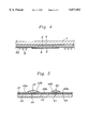
FIG. 4 is a fragmentary sectional view of a second embodiment of the present invention;
FIG. 5 is a view similar to FIG. 4 showing a third embodiment of the present invention;
FIG. 6 is a graph comparing the thermal strain applied to the IC chip when different base materials are used; and
FIG. 7 is a graph showing the thermal strain applied to the IC chip when different bonding agents are used for attaching the IC chip to an aluminum base.
FIGS. 1 to 3 show a first embodiment of the present invention which is constructed as a metal ball grid array semiconductor package. This semiconductor package is provided with a generally flat and square configuration, and comprises a metal base 1 consisting of an aluminum plate formed into a shallow rectangular pan, and an annular multi-layer circuit board 2, having a rectangular outer periphery and a rectangular central opening 2a, which is attached to the recessed surface 1a of the metal base 1. A semiconductor chip consisting of an IC chip 3 is attached to a part of the recessed surface 1a of the metal base 1 which is exposed by the central opening 2a of the circuit board 2 via a bonding layer 4 consisting of electroconductive silicone resin. A resin sealant 5 is filled into the central opening 2a of the circuit board 2 to thereby encapsulate the IC chip 3 in the resin sealant 5. The outer surface of the resin sealant 5 is covered by a metal cap layer 6. Because the IC chip 3 is attached to the metal base 1 with the bonding layer 4 consisting of the silicone resin layer which serves as a buffer layer, the difference in the thermal expansion coefficient between the metal base 1 and the IC chip 3 is absorbed by the silicone resin bonding layer 4, and the IC chip 3 is protected from any excessive thermal strain.
The bonding layer 4 may consist of film made of any material having some resiliency and a thermal conductivity as long as it is capable of absorbing any difference in the thermal expansion between the metal base and the IC chip so as not to apply any excessive thermal stress to the IC chip 3. This film, when cured, preferably has (1) a Young's modulus of 1,000 kgf/cm 2 or less, (2) an elongation of 30% or more, (3) a bonding force of 10 kgf/cm2 or more, and (4) a thermal conductivity of 1.0 W/m·K or more. If the Young's modulus is greater than 1,000 kgf/cm2 or the elongation is less than 30%, the IC chip may be subjected to an excessive thermal stress which may lead to a failure of the IC chip 3 to operate properly. If the bonding force is less than 10 kgf/cm2, repeated cyclic thermal stress that may be applied to the resin bonding layer 4 may lead to the separation of the IC chip 3. If the thermal conductivity is less than 1.0 W/m·K, the resulting insufficiency in heat dissipation may lead to improper operation of the IC chip 3.
More specifically, the resin bonding layer 4 may consist of a silicone bonding agent which is mixed with silver filler for electroconductivity. This bonding agent is applied to the surface of the metal base to the thickness of 20 to 50 μm, and turns elastomeric upon curing. As long as the preferred range of properties mentioned above is met, the filler which is mixed in the bonding agent may consist of materials other than Ag, or no filler may even be necessary. The thickness of the resin film may be also freely selected from the range of 5 μm to 500 μm so as to achieve a required bonding force and thermal conductivity.
The multi-layer circuit board 2 is provided with a number of through holes 2b. A plurality of pins 1b extend upright from the recessed surface 1a of the metal base 1. These pins 1b may be preferably formed by plastic deformation of the material of the metal base 1 although it is also possible to attach separate pins in such an upright arrangement. In this embodiment, the integrally formed pins 1b are each 0.3 mm in diameter and 0.3 mm in length, and 16 of them are arranged in suitable locations of the recessed surface 1a of the metal base 1 as best illustrated in FIG. 3. These pins 1b are fitted into corresponding through holes 2b provided in the circuit board 2 so as to serve as locating means for the circuit board 2. The through holes 2b into which the pins 1b are fitted are later filled by electroconductive paste 7 which electrically connects the pins to lands 8 and solder balls 9 formed on the outer surface of the circuit board 2.
The multi-layer circuit board 2 comprises a power line layer 21, a first circuit layer 22, a ground layer 23 serving as a separating layer for circuit layers, and a second circuit layer 24, in that order from the recessed surface 1a of the metal base 1. The inner periphery of the circuit board 2 surrounding the central opening 2a defines two approximately 1 mm wide steps 22a and 24a which are flush with the first and second circuit layers 22 and 24. Pads 22b and 24b for providing external connections for the corresponding circuit layers 22 and 24 are formed on these steps 22b and 24b, and are connected to corresponding pads 22a and 23a of the IC chip 3 by bonding wires 10. The through holes 2b may be connected to various parts of the first and second circuit layers 22 and 24 and the ground layer 23 via through hole plating applied to the thorough holes as required.
An approximately 1 mm wide gap is defined between the inner periphery of the opening 2a of the circuit board 2 and the outer periphery of the IC chip 3, and the surface of the metal base 1 in this gap is exposed. At least one bonding wire 11 is connected between the IC chip 3 and the exposed surface of this part of the metal base 1. Therefore, the ground line of the IC chip 3 can be connected to an external circuit such as a mother board via the metal base 1, the pins 1b, the through holes 2b (electroconductive paste 7), the lands 8, and the solder balls 9 for re-flow soldering. Normally, the through holes 2b into which the pins 1b are fitted are connected to the ground layer 23 for circuit separation.
FIG. 4 is a sectional view of a second embodiment of the present invention constructed as a metal ball grid array semiconductor package. In this embodiment, a single layer circuit board 32 made of glass-epoxy resin is used instead of the multi-layer circuit board 2 of the first embodiment. This arrangement is suited for IC chips which require a relatively small number of connecting pads, and, accordingly, the packaging arrangement can be made at a relatively low cost. In this embodiment, an IC chip 3 is attached to one side of a planar metal base 1 via a silicone resin bonding layer 4. The IC chip 3 is surrounded by a circuit board 32. The inner opening of the circuit board 2 is filled with a sealant 5, and the sealant is deposited beyond the height of the circuit board 32. A metal cap layer 6 is attached to the top surface (which is located at the lower end of the epoxy sealant layer 5 in FIG. 4) of the sealant layer 5. Bonding wires are connected between the bonding pads of the IC chip and the bonding pads formed on the circuit layer of the circuit board 2, and solder balls 9 are formed on corresponding electroconducitve lands of the surface circuit layer.
The above described embodiments were applied to ball grid array arrangements, but it is obvious for a person skilled in the art that the present invention can be equally applied to pin grid array arrangements simply by replacing the solder balls with terminal pins. If the surface of the IC chip opposing the metal base serves as a grounding pad, there will be no need for connecting the ground bonding pad of the IC chip to the metal base with a bonding wire if the IC chip is attached to be metal base with an electroconductive bonding layer. According to the first embodiment, because the pins projecting from the aluminum base can suffice for the grounding connections, it is possible to totally eliminate any other grounding connections.
FIG. 5 shows a third embodiment of the present invention applied to a metal circuit board arrangement. An insulating layer 42 is formed over the surface of a metal base 41, and a circuit layer 42a consisting of an electroconductive layer is formed over the surface of the insulating layer 42. A number of openings 42b are formed in the insulating layer 42, and electronic components 43, which may consist of passive chip components or semiconductor chip components, are each attached to the surface of the metal base 1 exposed by the corresponding opening 42b via a resin bonding layer 44. The resin bonding layer 4 is provided with the properties discussed in conjunction with the resin layer 4 of the first embodiment.
FIGS. 6 and 7 compare the thermal strains of an IC chip when it is attached to a metal base and a ceramic base by using different bonding methods including those using the resin bonding layer according to the present invention, solder, and epoxy bonding agents. The material properties of the silicone resin bonding agents according to the present invention, and the epoxy resin bonding agents for comparison are summarized in Table 2.
              TABLE 2
______________________________________
       silicone bonding agent
                   epoxy bonding agent
       mixed with silver filler
                   without filler
                             with silver filler
       A      B        C         D
______________________________________
Young's  100      200      5000    5000
modulus
(kgf/cm.sup.2)
elongation (%)
          50       30       5       5
bonding shear
          35       23      200      94
strength
(kgf/cm.sup.2)
thermal     1.3      2.1      1.02    2.8
conductivity
(W/m · K)
______________________________________
The comparison test was conducted by attaching a 12 mm by 12 mm IC chip centrally onto a surface of a 40×40×1.0 mm aluminum metal base and a ceramic base of a same size. A temperature compensated strain gauge was attached to the surface of the IC chip. This testing fixture was placed in an oven, and the resulting thermal strain was measured over the temperature range of from 25° C. (ambient temperature) to 120° C. at the increment of 5° C.
The results shown in FIG. 6 indicate that the arrangement according to the present invention gives rise to a substantially controlled thermal strain comparable to that produced when the IC chip is soldered to a ceramic base having a thermal expansion coefficient similar to that of the IC chip. The steep chain dot line and the "x" plots correspond to the measured and computed thermal strain of the aluminum base itself. The graph also includes the curves corresponding to the computed and measured thermal strains of a ceramic base itself.
FIG. 8 indicates that the present invention produces substantially smaller thermal strains than the arrangements in which the IC chip is mounted on an aluminum base by using epoxy bonding agents. Cyclic heat loading was also applied to the various fixtures, and it was found that the epoxy bonding agents degraded (separation of the IC chip and development of cracks in the bonding agent layer) in time due to thermal stress and absorption of moisture. On the other hand, the fixture according to the present invention using the resilient and heat conductive bonding agents consistently performed satisfactorily, and did not result in any defective conditions.
Thus, according to the present invention, the base may be made of a metal or an alloy such as aluminum which has a capability to favorably dissipate heat but has a large thermal expansion coefficient while avoiding the problem of causing excessive thermal strain to the electronic component because the resiliency of the bonding layer accommodates the thermal strain of the metal base. Because the bonding layer is highly heat conductive, the heat produced in the electronic component chip can be favorably transmitted to the metal base. It is therefore possible to achieve a high reliability in the packaging of semiconductor devices or the like at a minimum cost.
Although the present invention has been described in terms of specific embodiments thereof, it is possible to modify and alter details thereof without departing from the spirit of the present invention.
Claims (5)
1. A metallic electronic component packaging arrangement, comprising:
a metal base made of metal or alloy;
an electronic component chip securely mounted on said metal base with a bonding layer interposed between said chip and said metal base;
a circuit board placed on said metal base adjacent to said electronic component chip;
a bonding wire connected between a pad provided on said electronic component chip and a pad provided on said circuit board;
said bonding layer interposed between said metal base and said chip consisting of a resilient and heat conductive material which can prevent thermal strain of said metal base from adversely affecting said electronic component chip; and
wherein said metal base is provided with a projection, and said circuit board is provided with a through hole which is adapted to receive said projection when said circuit board is mounted on said metal base.
2. A metallic electronic component packaging arrangement according to claim 1, wherein said projection is adapted to locate said circuit board on said metal base.
3. A metallic electronic component packaging arrangement according to claim 2, wherein said projection provides a path for connecting a pad of said circuit board to said metal base.
4. A metallic electronic component packaging arrangement according to claim 3, wherein said projection is formed by plastic deformation of said metal base.
5. A metallic electronic component packaging arrangement comprising:
a metal base made of metal or alloy;
an electronic component chip securely mounted on said metal base with a bonding layer interposed between said chip and said metal base;
a circuit board placed on said metal base adjacent to said electronic component chip;
a bonding wire connected between a pad provided on said electronic component chip and a pad provided on said circuit board;
said bonding layer interposed between said metal base and said chip consisting of a resilient and heat conductive material which can prevent thermal strain of said metal base from adversely affecting said electronic component chip;
wherein said resilient and heat conductive material comprises silicone resin mixed with metal powder;
wherein said metal base comprises a shallow rectangular pan, having a recessed surface and said circuit board comprises an annular circuit board with a central aperture, said circuit board being attached to said recessed surface and said electronic component chip being mounted in said aperture; and
wherein an inner periphery of said circuit board, said electronic component chip and said bond wire are encapsulated with a resin sealant and are covered with a metal cap layer.
Applications Claiming Priority (6)
| Application Number | Priority Date | Filing Date | Title |
|---|---|---|---|
| JP7-306720 | 1995-10-31 | ||
| JP30672095 | 1995-10-31 | ||
| JP8-079435 | 1996-03-06 | ||
| JP8079435A JPH09186266A (en) | 1995-10-31 | 1996-03-06 | Semiconductor package |
| JP8-238612 | 1996-08-21 | ||
| JP8238612A JPH1064928A (en) | 1996-08-21 | 1996-08-21 | Semiconductor device using metal base |
Publications (1)
| Publication Number | Publication Date |
|---|---|
| US5877553A true US5877553A (en) | 1999-03-02 |
Family
ID=27303020
Family Applications (1)
| Application Number | Title | Priority Date | Filing Date |
|---|---|---|---|
| US08/739,662 Expired - Fee Related US5877553A (en) | 1995-10-31 | 1996-10-31 | Metallic electronic component packaging arrangement |
Country Status (3)
| Country | Link |
|---|---|
| US (1) | US5877553A (en) |
| KR (1) | KR100271836B1 (en) |
| TW (1) | TW363262B (en) |
Cited By (9)
| Publication number | Priority date | Publication date | Assignee | Title |
|---|---|---|---|---|
| US6153829A (en) * | 1998-09-15 | 2000-11-28 | Intel Corporation | Split cavity wall plating for an integrated circuit package |
| US6249053B1 (en) * | 1998-02-16 | 2001-06-19 | Sumitomo Metal (Smi) Electronics Devices Inc. | Chip package and method for manufacturing the same |
| US20020132443A1 (en) * | 2001-03-05 | 2002-09-19 | Winther Kaspar Tobias | Bonding of parts with dissimilar thermal expansion coefficients |
| US20020142574A1 (en) * | 2001-04-02 | 2002-10-03 | Shu-Hui Chen | Solder ball allocation on a chip and method of the same |
| US6495394B1 (en) | 1999-02-16 | 2002-12-17 | Sumitomo Metal (Smi) Electronics Devices Inc. | Chip package and method for manufacturing the same |
| US20030087448A1 (en) * | 2001-11-07 | 2003-05-08 | Hitachi, Ltd | Electronic device and thermal type flow meter on vehicle |
| US20040046243A1 (en) * | 1998-09-15 | 2004-03-11 | Carapella Elissa E. | Methods of split cavity wall plating for an integrated circuit package |
| US20100019380A1 (en) * | 2008-07-24 | 2010-01-28 | Yi Min Lin | Integrated circuit with micro-pores ceramic heat sink |
| CN109155288A (en) * | 2016-05-20 | 2019-01-04 | 京瓷株式会社 | Electronic component mounting substrate and electronic device |
Citations (10)
| Publication number | Priority date | Publication date | Assignee | Title |
|---|---|---|---|---|
| US4314270A (en) * | 1977-12-02 | 1982-02-02 | Mitsubishi Denki Kabushiki Kaisha | Hybrid thick film integrated circuit heat dissipating and grounding assembly |
| US4381469A (en) * | 1979-07-20 | 1983-04-26 | Murata Manufacturing Company, Ltd. | Temperature stable piezoelectric device |
| US4577056A (en) * | 1984-04-09 | 1986-03-18 | Olin Corporation | Hermetically sealed metal package |
| US4663649A (en) * | 1982-06-16 | 1987-05-05 | Hitachi, Ltd. | SiC sintered body having metallized layer and production method thereof |
| US5023398A (en) * | 1988-10-05 | 1991-06-11 | Olin Corporation | Aluminum alloy semiconductor packages |
| US5317194A (en) * | 1989-10-17 | 1994-05-31 | Kabushiki Kaisha Toshiba | Resin-sealed semiconductor device having intermediate silicon thermal dissipation means and embedded heat sink |
| US5344498A (en) * | 1991-10-08 | 1994-09-06 | Canon Kabushiki Kaisha | Solar cell module with improved weathering characteristics |
| US5367196A (en) * | 1992-09-17 | 1994-11-22 | Olin Corporation | Molded plastic semiconductor package including an aluminum alloy heat spreader |
| US5552637A (en) * | 1993-06-14 | 1996-09-03 | Kabushiki Kaisha Toshiba | Semiconductor device |
| US5641997A (en) * | 1993-09-14 | 1997-06-24 | Kabushiki Kaisha Toshiba | Plastic-encapsulated semiconductor device |
Family Cites Families (1)
| Publication number | Priority date | Publication date | Assignee | Title |
|---|---|---|---|---|
| JP3253154B2 (en) * | 1993-01-06 | 2002-02-04 | 新光電気工業株式会社 | Package for semiconductor device and semiconductor device |
-
1996
- 1996-10-29 TW TW085113187A patent/TW363262B/en active
- 1996-10-30 KR KR1019960050001A patent/KR100271836B1/en not_active IP Right Cessation
- 1996-10-31 US US08/739,662 patent/US5877553A/en not_active Expired - Fee Related
Patent Citations (10)
| Publication number | Priority date | Publication date | Assignee | Title |
|---|---|---|---|---|
| US4314270A (en) * | 1977-12-02 | 1982-02-02 | Mitsubishi Denki Kabushiki Kaisha | Hybrid thick film integrated circuit heat dissipating and grounding assembly |
| US4381469A (en) * | 1979-07-20 | 1983-04-26 | Murata Manufacturing Company, Ltd. | Temperature stable piezoelectric device |
| US4663649A (en) * | 1982-06-16 | 1987-05-05 | Hitachi, Ltd. | SiC sintered body having metallized layer and production method thereof |
| US4577056A (en) * | 1984-04-09 | 1986-03-18 | Olin Corporation | Hermetically sealed metal package |
| US5023398A (en) * | 1988-10-05 | 1991-06-11 | Olin Corporation | Aluminum alloy semiconductor packages |
| US5317194A (en) * | 1989-10-17 | 1994-05-31 | Kabushiki Kaisha Toshiba | Resin-sealed semiconductor device having intermediate silicon thermal dissipation means and embedded heat sink |
| US5344498A (en) * | 1991-10-08 | 1994-09-06 | Canon Kabushiki Kaisha | Solar cell module with improved weathering characteristics |
| US5367196A (en) * | 1992-09-17 | 1994-11-22 | Olin Corporation | Molded plastic semiconductor package including an aluminum alloy heat spreader |
| US5552637A (en) * | 1993-06-14 | 1996-09-03 | Kabushiki Kaisha Toshiba | Semiconductor device |
| US5641997A (en) * | 1993-09-14 | 1997-06-24 | Kabushiki Kaisha Toshiba | Plastic-encapsulated semiconductor device |
Cited By (16)
| Publication number | Priority date | Publication date | Assignee | Title |
|---|---|---|---|---|
| US6620650B2 (en) | 1998-02-16 | 2003-09-16 | Sumitomo Metal (Smi) Electronics Devices Inc. | Chip package and method for manufacturing the same |
| US6249053B1 (en) * | 1998-02-16 | 2001-06-19 | Sumitomo Metal (Smi) Electronics Devices Inc. | Chip package and method for manufacturing the same |
| US7020958B1 (en) * | 1998-09-15 | 2006-04-04 | Intel Corporation | Methods forming an integrated circuit package with a split cavity wall |
| US20040046243A1 (en) * | 1998-09-15 | 2004-03-11 | Carapella Elissa E. | Methods of split cavity wall plating for an integrated circuit package |
| US6153829A (en) * | 1998-09-15 | 2000-11-28 | Intel Corporation | Split cavity wall plating for an integrated circuit package |
| US6495394B1 (en) | 1999-02-16 | 2002-12-17 | Sumitomo Metal (Smi) Electronics Devices Inc. | Chip package and method for manufacturing the same |
| US6897123B2 (en) | 2001-03-05 | 2005-05-24 | Agityne Corporation | Bonding of parts with dissimilar thermal expansion coefficients |
| US20020132443A1 (en) * | 2001-03-05 | 2002-09-19 | Winther Kaspar Tobias | Bonding of parts with dissimilar thermal expansion coefficients |
| US6696763B2 (en) * | 2001-04-02 | 2004-02-24 | Via Technologies, Inc. | Solder ball allocation on a chip and method of the same |
| US20020142574A1 (en) * | 2001-04-02 | 2002-10-03 | Shu-Hui Chen | Solder ball allocation on a chip and method of the same |
| US20030087448A1 (en) * | 2001-11-07 | 2003-05-08 | Hitachi, Ltd | Electronic device and thermal type flow meter on vehicle |
| US20070025878A1 (en) * | 2001-11-07 | 2007-02-01 | Hitachi, Ltd. | Electronic device and thermal type flow meter on vehicle |
| US7255837B2 (en) * | 2001-11-07 | 2007-08-14 | Hitachi, Ltd. | Electronic device and thermal type flow meter on vehicle |
| US20100019380A1 (en) * | 2008-07-24 | 2010-01-28 | Yi Min Lin | Integrated circuit with micro-pores ceramic heat sink |
| CN109155288A (en) * | 2016-05-20 | 2019-01-04 | 京瓷株式会社 | Electronic component mounting substrate and electronic device |
| CN109155288B (en) * | 2016-05-20 | 2022-02-08 | 京瓷株式会社 | Substrate for mounting electronic component and electronic device |
Also Published As
| Publication number | Publication date |
|---|---|
| TW363262B (en) | 1999-07-01 |
| KR100271836B1 (en) | 2000-11-15 |
| KR970024043A (en) | 1997-05-30 |
Similar Documents
| Publication | Publication Date | Title |
|---|---|---|
| US10204848B2 (en) | Semiconductor chip package having heat dissipating structure | |
| JP3437369B2 (en) | Chip carrier and semiconductor device using the same | |
| US6956741B2 (en) | Semiconductor package with heat sink | |
| US5602059A (en) | Semiconductor device and method for manufacturing same | |
| US5581122A (en) | Packaging assembly with consolidated common voltage connections for integrated circuits | |
| KR100310398B1 (en) | Pad Array Semiconductor Device with Thermal Conductor and Manufacturing Method Thereof | |
| US6359341B1 (en) | Ball grid array integrated circuit package structure | |
| US5397921A (en) | Tab grid array | |
| US5598031A (en) | Electrically and thermally enhanced package using a separate silicon substrate | |
| US6028354A (en) | Microelectronic device package having a heat sink structure for increasing the thermal conductivity of the package | |
| US6818978B1 (en) | Ball grid array package with shielding | |
| KR100694739B1 (en) | Ball grid array package with multiple power/ground planes | |
| KR100302537B1 (en) | Semiconductor device | |
| EP1796163B1 (en) | Semiconductor device and electronic control unit using the same | |
| US20020105070A1 (en) | Semiconductor device, manufacturing method thereof and mounting board | |
| WO1999062119A1 (en) | Rf shielded electronic device | |
| JPH10308466A (en) | Ball grid array semiconductor package with heat sink | |
| US6130477A (en) | Thin enhanced TAB BGA package having improved heat dissipation | |
| US20040004281A1 (en) | Semiconductor package with heat sink | |
| WO2004043130A2 (en) | Mechanically enhanced package and method of making same | |
| US5877553A (en) | Metallic electronic component packaging arrangement | |
| US6166435A (en) | Flip-chip ball grid array package with a heat slug | |
| KR101096330B1 (en) | Package for a semiconductor device | |
| US6351389B1 (en) | Device and method for packaging an electronic device | |
| JP2002231850A (en) | Semiconductor device storing wiring board |
Legal Events
| Date | Code | Title | Description |
|---|---|---|---|
| AS | Assignment |
Owner name: NHK SPRING CO., LTD., JAPAN Free format text: ASSIGNMENT OF ASSIGNORS INTEREST;ASSIGNORS:NAKAYAMA, OSAMU;ISHIKAWA, KOJI;REEL/FRAME:008297/0417 Effective date: 19961023 |
|
| REMI | Maintenance fee reminder mailed | ||
| LAPS | Lapse for failure to pay maintenance fees | ||
| STCH | Information on status: patent discontinuation |
Free format text: PATENT EXPIRED DUE TO NONPAYMENT OF MAINTENANCE FEES UNDER 37 CFR 1.362 |
|
| FP | Lapsed due to failure to pay maintenance fee |
Effective date: 20030302 |