US5883015A - Method for using oxygen plasma treatment on a dielectric layer - Google Patents
Method for using oxygen plasma treatment on a dielectric layer Download PDFInfo
- Publication number
- US5883015A US5883015A US08/887,886 US88788697A US5883015A US 5883015 A US5883015 A US 5883015A US 88788697 A US88788697 A US 88788697A US 5883015 A US5883015 A US 5883015A
- Authority
- US
- United States
- Prior art keywords
- vapor deposition
- chemical vapor
- dielectric film
- substrate
- dielectric layer
- Prior art date
- Legal status (The legal status is an assumption and is not a legal conclusion. Google has not performed a legal analysis and makes no representation as to the accuracy of the status listed.)
- Expired - Lifetime
Links
Images

Classifications
-
- H—ELECTRICITY
- H01—ELECTRIC ELEMENTS
- H01L—SEMICONDUCTOR DEVICES NOT COVERED BY CLASS H10
- H01L21/00—Processes or apparatus adapted for the manufacture or treatment of semiconductor or solid state devices or of parts thereof
- H01L21/02—Manufacture or treatment of semiconductor devices or of parts thereof
- H01L21/02104—Forming layers
- H01L21/02107—Forming insulating materials on a substrate
- H01L21/02109—Forming insulating materials on a substrate characterised by the type of layer, e.g. type of material, porous/non-porous, pre-cursors, mixtures or laminates
- H01L21/02112—Forming insulating materials on a substrate characterised by the type of layer, e.g. type of material, porous/non-porous, pre-cursors, mixtures or laminates characterised by the material of the layer
- H01L21/02123—Forming insulating materials on a substrate characterised by the type of layer, e.g. type of material, porous/non-porous, pre-cursors, mixtures or laminates characterised by the material of the layer the material containing silicon
- H01L21/02164—Forming insulating materials on a substrate characterised by the type of layer, e.g. type of material, porous/non-porous, pre-cursors, mixtures or laminates characterised by the material of the layer the material containing silicon the material being a silicon oxide, e.g. SiO2
-
- C—CHEMISTRY; METALLURGY
- C23—COATING METALLIC MATERIAL; COATING MATERIAL WITH METALLIC MATERIAL; CHEMICAL SURFACE TREATMENT; DIFFUSION TREATMENT OF METALLIC MATERIAL; COATING BY VACUUM EVAPORATION, BY SPUTTERING, BY ION IMPLANTATION OR BY CHEMICAL VAPOUR DEPOSITION, IN GENERAL; INHIBITING CORROSION OF METALLIC MATERIAL OR INCRUSTATION IN GENERAL
- C23C—COATING METALLIC MATERIAL; COATING MATERIAL WITH METALLIC MATERIAL; SURFACE TREATMENT OF METALLIC MATERIAL BY DIFFUSION INTO THE SURFACE, BY CHEMICAL CONVERSION OR SUBSTITUTION; COATING BY VACUUM EVAPORATION, BY SPUTTERING, BY ION IMPLANTATION OR BY CHEMICAL VAPOUR DEPOSITION, IN GENERAL
- C23C16/00—Chemical coating by decomposition of gaseous compounds, without leaving reaction products of surface material in the coating, i.e. chemical vapour deposition [CVD] processes
- C23C16/22—Chemical coating by decomposition of gaseous compounds, without leaving reaction products of surface material in the coating, i.e. chemical vapour deposition [CVD] processes characterised by the deposition of inorganic material, other than metallic material
- C23C16/30—Deposition of compounds, mixtures or solid solutions, e.g. borides, carbides, nitrides
- C23C16/40—Oxides
- C23C16/401—Oxides containing silicon
- C23C16/402—Silicon dioxide
-
- H—ELECTRICITY
- H01—ELECTRIC ELEMENTS
- H01L—SEMICONDUCTOR DEVICES NOT COVERED BY CLASS H10
- H01L21/00—Processes or apparatus adapted for the manufacture or treatment of semiconductor or solid state devices or of parts thereof
- H01L21/02—Manufacture or treatment of semiconductor devices or of parts thereof
- H01L21/02104—Forming layers
- H01L21/02107—Forming insulating materials on a substrate
- H01L21/02109—Forming insulating materials on a substrate characterised by the type of layer, e.g. type of material, porous/non-porous, pre-cursors, mixtures or laminates
- H01L21/022—Forming insulating materials on a substrate characterised by the type of layer, e.g. type of material, porous/non-porous, pre-cursors, mixtures or laminates the layer being a laminate, i.e. composed of sublayers, e.g. stacks of alternating high-k metal oxides
-
- H—ELECTRICITY
- H01—ELECTRIC ELEMENTS
- H01L—SEMICONDUCTOR DEVICES NOT COVERED BY CLASS H10
- H01L21/00—Processes or apparatus adapted for the manufacture or treatment of semiconductor or solid state devices or of parts thereof
- H01L21/02—Manufacture or treatment of semiconductor devices or of parts thereof
- H01L21/02104—Forming layers
- H01L21/02107—Forming insulating materials on a substrate
- H01L21/02225—Forming insulating materials on a substrate characterised by the process for the formation of the insulating layer
- H01L21/0226—Forming insulating materials on a substrate characterised by the process for the formation of the insulating layer formation by a deposition process
- H01L21/02263—Forming insulating materials on a substrate characterised by the process for the formation of the insulating layer formation by a deposition process deposition from the gas or vapour phase
- H01L21/02271—Forming insulating materials on a substrate characterised by the process for the formation of the insulating layer formation by a deposition process deposition from the gas or vapour phase deposition by decomposition or reaction of gaseous or vapour phase compounds, i.e. chemical vapour deposition
- H01L21/02274—Forming insulating materials on a substrate characterised by the process for the formation of the insulating layer formation by a deposition process deposition from the gas or vapour phase deposition by decomposition or reaction of gaseous or vapour phase compounds, i.e. chemical vapour deposition in the presence of a plasma [PECVD]
-
- H—ELECTRICITY
- H01—ELECTRIC ELEMENTS
- H01L—SEMICONDUCTOR DEVICES NOT COVERED BY CLASS H10
- H01L21/00—Processes or apparatus adapted for the manufacture or treatment of semiconductor or solid state devices or of parts thereof
- H01L21/02—Manufacture or treatment of semiconductor devices or of parts thereof
- H01L21/02104—Forming layers
- H01L21/02107—Forming insulating materials on a substrate
- H01L21/02296—Forming insulating materials on a substrate characterised by the treatment performed before or after the formation of the layer
- H01L21/02318—Forming insulating materials on a substrate characterised by the treatment performed before or after the formation of the layer post-treatment
- H01L21/02337—Forming insulating materials on a substrate characterised by the treatment performed before or after the formation of the layer post-treatment treatment by exposure to a gas or vapour
- H01L21/0234—Forming insulating materials on a substrate characterised by the treatment performed before or after the formation of the layer post-treatment treatment by exposure to a gas or vapour treatment by exposure to a plasma
-
- H—ELECTRICITY
- H01—ELECTRIC ELEMENTS
- H01L—SEMICONDUCTOR DEVICES NOT COVERED BY CLASS H10
- H01L21/00—Processes or apparatus adapted for the manufacture or treatment of semiconductor or solid state devices or of parts thereof
- H01L21/02—Manufacture or treatment of semiconductor devices or of parts thereof
- H01L21/04—Manufacture or treatment of semiconductor devices or of parts thereof the devices having at least one potential-jump barrier or surface barrier, e.g. PN junction, depletion layer or carrier concentration layer
- H01L21/18—Manufacture or treatment of semiconductor devices or of parts thereof the devices having at least one potential-jump barrier or surface barrier, e.g. PN junction, depletion layer or carrier concentration layer the devices having semiconductor bodies comprising elements of Group IV of the Periodic System or AIIIBV compounds with or without impurities, e.g. doping materials
- H01L21/30—Treatment of semiconductor bodies using processes or apparatus not provided for in groups H01L21/20 - H01L21/26
- H01L21/31—Treatment of semiconductor bodies using processes or apparatus not provided for in groups H01L21/20 - H01L21/26 to form insulating layers thereon, e.g. for masking or by using photolithographic techniques; After treatment of these layers; Selection of materials for these layers
- H01L21/314—Inorganic layers
- H01L21/316—Inorganic layers composed of oxides or glassy oxides or oxide based glass
- H01L21/31604—Deposition from a gas or vapour
- H01L21/31608—Deposition of SiO2
- H01L21/31612—Deposition of SiO2 on a silicon body
Definitions
- the present invention is related to a method for depositing a dielectric layer, and especially relates to a method for evenly depositing a dielectric layer which can be applied to the semiconductor device.
- the dielectric layer can be formed by deposition or non-deposition (e.g. thermal oxidation).
- deposition or non-deposition e.g. thermal oxidation
- PVD physical vapor deposition
- CVD chemical vapor deposition
- the chemical vapor deposition can be classified into atmospheric pressure chemical vapor deposition (APCVD), sub-atmospheric pressure chemical vapor deposition (SACVD), low pressure chemical vapor deposition (LPCVD), and plasma enhanced chemical vapor deposition (PECVD).
- APCVD atmospheric pressure chemical vapor deposition
- SACVD sub-atmospheric pressure chemical vapor deposition
- LPCVD low pressure chemical vapor deposition
- PECVD plasma enhanced chemical vapor deposition
- the major source of reaction gas containing silicon is silane (SiH 4 ) or tetra-ethylortho-silicate (TEOS).
- the dielectric layer formed by low pressure chemical vapor deposition (LPCVD) using TEOS
- LPCVD low pressure chemical vapor deposition
- TEOS TEOS
- PECVD plasma enhanced chemical vapor deposition
- APCVD atmospheric pressure chemical vapor deposition
- An object of the present invention is to provide a method for evenly depositing a dielectric layer which can be applied to, the semiconductor device.
- a method provided by the present invention for depositing a dielectric layer includes steps of: a) providing a substrate; b) depositing a first dielectric film on the subtrate; c) introducing an oxygen plasma for eliminating an uneven distribution of charges on a surface of the substrate, and d) forming a second dielectric film on the first dielectric film treated with the oxygen plasma for obtaining the dielectric layer having a uniform thickness on the substrate.
- the substrate has a polysilicon gate structure thereon.
- the first dielectric film is formed by a plasma enhanced chemical vapor deposition (PECVD).
- PECVD plasma enhanced chemical vapor deposition
- TEOS tetraethyl-ortho-silicate
- the first dielectric film is made of silicon dioxide.
- a pressure of the introduced oxygen plasma is ranged between 3 and 14 torr.
- a pressure of the introduced oxygen plasma is 8.2 torr.
- the second dielectric film is formed by a chemical vapor deposition (CVD).
- the chemical vapor deposition is one selected from a group consisted of an atmospheric pressure chemical vapor deposition and a subatmospheric pressure chemical vapor deposition, both of which use ozone.
- TEOS tetra ethyl-ortho-silicate
- the second dielectric film is made of silicon dioxide.
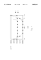
- FIG. 1 is a comparison diagram of the oxide charge distribution of the dielectric layer between the conventional process and the present invention according to the data of surface charge analyzer, wherein the distance between the substrate and the plasma outlet is 280 mils; curve A is formed under 8.2 torr and curve B is formed under 1 torr; and
- FIG. 2 is a comparison diagram for the oxide charge distribution of the dielectric layer between the conventional process and the present invention according to the data of surface charge analyzer, wherein the distance between the substrate and the plasma outlet is 780 mils; curve C is formed under 8.2 torr and curve D is formed under 1 torr,
- the dielectric layer SiO 2
- the thickness uniformity of O 3 /TEOS process is closely related to the under layer formed during the PECVD/TEOS procedure.
- the deposition thickness of the dielectric layer on the wafer varies with the distance to the center of the wafer, as illustrated by curve B and D respectively shown in FIG. 1 and FIG. 2, resulting from charge residues after PECVD/TEOS process.
- FIG. 1 is a charge residue distribution diagram of the dielectric layer, wherein the distance between the substrate and the plasma outlet is 280 mils; curve A is formed under 8.2 torr and curve B is formed under 1 torr.
- FIG. 2 is a charge residue distribution diagram of the dielectric layer, wherein the distance between the substrate and the plasma outlet is 780 mils; curve C is formed under 8.2 torr and curve D is formed under 1 torr.
- the present invention provides a method for depositing a dielectric layer which can evenly deposit the dielectric layer to be applied to the semiconductor device.
- the method of the present invention includes steps of: (a) providing a substrate; (b) depositing a first dielectric film on the, substrate; (c) introducing an oxygen plasma for eliminating an uneven distribution of charges on a surface of the substrate; and (d) forming a second dielectric film on the first dielectric film treated with the oxygen plasma for obtaining the dielectric layer having a uniform thickness on the substrate.
- the substrate is made of silicon
- the desired dielectric layer is a silicon dioxide layer
- the reaction liquid source is tetra-ethyl-ortho-silicate (TEOS).
- TEOS tetra-ethyl-ortho-silicate
- the present invention provides a method which can greatly improves the defect of uneven charge distribution of the conventional method.
Abstract
Description
Claims (10)
Priority Applications (1)
| Application Number | Priority Date | Filing Date | Title |
|---|---|---|---|
| US08/887,886 US5883015A (en) | 1997-07-03 | 1997-07-03 | Method for using oxygen plasma treatment on a dielectric layer |
Applications Claiming Priority (1)
| Application Number | Priority Date | Filing Date | Title |
|---|---|---|---|
| US08/887,886 US5883015A (en) | 1997-07-03 | 1997-07-03 | Method for using oxygen plasma treatment on a dielectric layer |
Publications (1)
| Publication Number | Publication Date |
|---|---|
| US5883015A true US5883015A (en) | 1999-03-16 |
Family
ID=25392074
Family Applications (1)
| Application Number | Title | Priority Date | Filing Date |
|---|---|---|---|
| US08/887,886 Expired - Lifetime US5883015A (en) | 1997-07-03 | 1997-07-03 | Method for using oxygen plasma treatment on a dielectric layer |
Country Status (1)
| Country | Link |
|---|---|
| US (1) | US5883015A (en) |
Cited By (2)
| Publication number | Priority date | Publication date | Assignee | Title |
|---|---|---|---|---|
| US6153512A (en) * | 1999-10-12 | 2000-11-28 | Taiwan Semiconductor Manufacturing Company | Process to improve adhesion of HSQ to underlying materials |
| CN104599961A (en) * | 2013-11-01 | 2015-05-06 | 上海华虹宏力半导体制造有限公司 | Method for reducing silicon oxynitride surface charges |
Citations (5)
| Publication number | Priority date | Publication date | Assignee | Title |
|---|---|---|---|---|
| US5554570A (en) * | 1994-01-25 | 1996-09-10 | Canon Sales Co., Inc. | Method of forming insulating film |
| US5556806A (en) * | 1995-06-28 | 1996-09-17 | Taiwan Semiconductor Manufacturing Company | Spin-on-glass nonetchback planarization process using oxygen plasma treatment |
| US5563104A (en) * | 1995-06-23 | 1996-10-08 | Taiwan Semiconductor Manufacturing Company Ltd. | Reduction of pattern sensitivity in ozone-teos deposition via a two-step (low and high temperature) process |
| US5605859A (en) * | 1995-07-05 | 1997-02-25 | Taiwan Semiconductor Manufacturing Company, Ltd. | Method of making insulator structure for polysilicon resistors |
| US5627403A (en) * | 1993-05-31 | 1997-05-06 | Sgs-Thomson Microelectronics S.R.L. | Adhesion between dielectric layers in an integrated circuit |
-
1997
- 1997-07-03 US US08/887,886 patent/US5883015A/en not_active Expired - Lifetime
Patent Citations (5)
| Publication number | Priority date | Publication date | Assignee | Title |
|---|---|---|---|---|
| US5627403A (en) * | 1993-05-31 | 1997-05-06 | Sgs-Thomson Microelectronics S.R.L. | Adhesion between dielectric layers in an integrated circuit |
| US5554570A (en) * | 1994-01-25 | 1996-09-10 | Canon Sales Co., Inc. | Method of forming insulating film |
| US5563104A (en) * | 1995-06-23 | 1996-10-08 | Taiwan Semiconductor Manufacturing Company Ltd. | Reduction of pattern sensitivity in ozone-teos deposition via a two-step (low and high temperature) process |
| US5556806A (en) * | 1995-06-28 | 1996-09-17 | Taiwan Semiconductor Manufacturing Company | Spin-on-glass nonetchback planarization process using oxygen plasma treatment |
| US5605859A (en) * | 1995-07-05 | 1997-02-25 | Taiwan Semiconductor Manufacturing Company, Ltd. | Method of making insulator structure for polysilicon resistors |
Cited By (3)
| Publication number | Priority date | Publication date | Assignee | Title |
|---|---|---|---|---|
| US6153512A (en) * | 1999-10-12 | 2000-11-28 | Taiwan Semiconductor Manufacturing Company | Process to improve adhesion of HSQ to underlying materials |
| CN104599961A (en) * | 2013-11-01 | 2015-05-06 | 上海华虹宏力半导体制造有限公司 | Method for reducing silicon oxynitride surface charges |
| CN104599961B (en) * | 2013-11-01 | 2017-10-20 | 上海华虹宏力半导体制造有限公司 | A kind of method for reducing silicon oxynitride film surface charge |
Similar Documents
| Publication | Publication Date | Title |
|---|---|---|
| US7582555B1 (en) | CVD flowable gap fill | |
| US5970383A (en) | Method of manufacturing a semiconductor device with improved control of deposition layer thickness | |
| US7939422B2 (en) | Methods of thin film process | |
| US5648175A (en) | Chemical vapor deposition reactor system and integrated circuit | |
| US6660662B2 (en) | Method of reducing plasma charge damage for plasma processes | |
| US6821572B2 (en) | Method of cleaning a chemical vapor deposition chamber | |
| KR100355914B1 (en) | Direct Circuit Manufacturing Method Using Low Temperature Plasma | |
| US7288284B2 (en) | Post-cleaning chamber seasoning method | |
| KR100743789B1 (en) | Barrier layer deposition using hdp-cvd | |
| US6486083B1 (en) | Semiconductor device manufacturing method and semiconductor manufacturing apparatus | |
| US6531413B2 (en) | Method for depositing an undoped silicate glass layer | |
| US20010029114A1 (en) | Method of forming polymeric layers of silicon oxynitride | |
| US6534409B1 (en) | Silicon oxide co-deposition/etching process | |
| US7384486B2 (en) | Chamber cleaning method | |
| US6436303B1 (en) | Film removal employing a remote plasma source | |
| KR20030074721A (en) | Plasma processing device and plasma processing method | |
| US5883015A (en) | Method for using oxygen plasma treatment on a dielectric layer | |
| US20010012701A1 (en) | Method of forming a silicon nitride thin film | |
| EP0935284A1 (en) | CVD of silicon containing film using Si2H6 | |
| US6090725A (en) | Method for preventing bubble defects in BPSG film | |
| JP3230185B2 (en) | Deposition method of uniform dielectric layer | |
| JPH0574763A (en) | Formation of gate insulating film | |
| US6713406B1 (en) | Method for depositing dielectric materials onto semiconductor substrates by HDP (high density plasma) CVD (chemical vapor deposition) processes without damage to FET active devices | |
| JP2657306B2 (en) | Method of forming metal silicide film | |
| KR20050018641A (en) | Low temperature dielectric deposition using aminosilane and ozone |
Legal Events
| Date | Code | Title | Description |
|---|---|---|---|
| AS | Assignment |
Owner name: MOSEL VITELIC INC., TAIWAN Free format text: ASSIGNMENT OF ASSIGNORS INTEREST;ASSIGNORS:LIAO, KENT;HUANG, DINOS;TU, TUBY;AND OTHERS;REEL/FRAME:008672/0170 Effective date: 19970701 |
|
| STCF | Information on status: patent grant |
Free format text: PATENTED CASE |
|
| FEPP | Fee payment procedure |
Free format text: PAYOR NUMBER ASSIGNED (ORIGINAL EVENT CODE: ASPN); ENTITY STATUS OF PATENT OWNER: LARGE ENTITY |
|
| FPAY | Fee payment |
Year of fee payment: 4 |
|
| AS | Assignment |
Owner name: PROMOS TECHNOLOGIES INC., TAIWAN Free format text: ASSIGNMENT OF ASSIGNORS INTEREST;ASSIGNOR:MOSEL VITELIC, INC.;REEL/FRAME:015334/0772 Effective date: 20040427 |
|
| FPAY | Fee payment |
Year of fee payment: 8 |
|
| FPAY | Fee payment |
Year of fee payment: 12 |