US5883473A - Electronic Ballast with inverter protection circuit - Google Patents
Electronic Ballast with inverter protection circuit Download PDFInfo
- Publication number
- US5883473A US5883473A US08/984,444 US98444497A US5883473A US 5883473 A US5883473 A US 5883473A US 98444497 A US98444497 A US 98444497A US 5883473 A US5883473 A US 5883473A
- Authority
- US
- United States
- Prior art keywords
- coupled
- input
- output
- circuit
- inverter
- Prior art date
- Legal status (The legal status is an assumption and is not a legal conclusion. Google has not performed a legal analysis and makes no representation as to the accuracy of the status listed.)
- Expired - Lifetime
Links
Images


Classifications
-
- H—ELECTRICITY
- H05—ELECTRIC TECHNIQUES NOT OTHERWISE PROVIDED FOR
- H05B—ELECTRIC HEATING; ELECTRIC LIGHT SOURCES NOT OTHERWISE PROVIDED FOR; CIRCUIT ARRANGEMENTS FOR ELECTRIC LIGHT SOURCES, IN GENERAL
- H05B41/00—Circuit arrangements or apparatus for igniting or operating discharge lamps
- H05B41/14—Circuit arrangements
- H05B41/26—Circuit arrangements in which the lamp is fed by power derived from dc by means of a converter, e.g. by high-voltage dc
- H05B41/28—Circuit arrangements in which the lamp is fed by power derived from dc by means of a converter, e.g. by high-voltage dc using static converters
- H05B41/282—Circuit arrangements in which the lamp is fed by power derived from dc by means of a converter, e.g. by high-voltage dc using static converters with semiconductor devices
- H05B41/285—Arrangements for protecting lamps or circuits against abnormal operating conditions
- H05B41/2851—Arrangements for protecting lamps or circuits against abnormal operating conditions for protecting the circuit against abnormal operating conditions
- H05B41/2855—Arrangements for protecting lamps or circuits against abnormal operating conditions for protecting the circuit against abnormal operating conditions against abnormal lamp operating conditions
-
- H—ELECTRICITY
- H05—ELECTRIC TECHNIQUES NOT OTHERWISE PROVIDED FOR
- H05B—ELECTRIC HEATING; ELECTRIC LIGHT SOURCES NOT OTHERWISE PROVIDED FOR; CIRCUIT ARRANGEMENTS FOR ELECTRIC LIGHT SOURCES, IN GENERAL
- H05B41/00—Circuit arrangements or apparatus for igniting or operating discharge lamps
- H05B41/14—Circuit arrangements
- H05B41/26—Circuit arrangements in which the lamp is fed by power derived from dc by means of a converter, e.g. by high-voltage dc
- H05B41/28—Circuit arrangements in which the lamp is fed by power derived from dc by means of a converter, e.g. by high-voltage dc using static converters
- H05B41/295—Circuit arrangements in which the lamp is fed by power derived from dc by means of a converter, e.g. by high-voltage dc using static converters with semiconductor devices and specially adapted for lamps with preheating electrodes, e.g. for fluorescent lamps
- H05B41/298—Arrangements for protecting lamps or circuits against abnormal operating conditions
- H05B41/2981—Arrangements for protecting lamps or circuits against abnormal operating conditions for protecting the circuit against abnormal operating conditions
- H05B41/2985—Arrangements for protecting lamps or circuits against abnormal operating conditions for protecting the circuit against abnormal operating conditions against abnormal lamp operating conditions
-
- Y—GENERAL TAGGING OF NEW TECHNOLOGICAL DEVELOPMENTS; GENERAL TAGGING OF CROSS-SECTIONAL TECHNOLOGIES SPANNING OVER SEVERAL SECTIONS OF THE IPC; TECHNICAL SUBJECTS COVERED BY FORMER USPC CROSS-REFERENCE ART COLLECTIONS [XRACs] AND DIGESTS
- Y10—TECHNICAL SUBJECTS COVERED BY FORMER USPC
- Y10S—TECHNICAL SUBJECTS COVERED BY FORMER USPC CROSS-REFERENCE ART COLLECTIONS [XRACs] AND DIGESTS
- Y10S315/00—Electric lamp and discharge devices: systems
- Y10S315/05—Starting and operating circuit for fluorescent lamp
-
- Y—GENERAL TAGGING OF NEW TECHNOLOGICAL DEVELOPMENTS; GENERAL TAGGING OF CROSS-SECTIONAL TECHNOLOGIES SPANNING OVER SEVERAL SECTIONS OF THE IPC; TECHNICAL SUBJECTS COVERED BY FORMER USPC CROSS-REFERENCE ART COLLECTIONS [XRACs] AND DIGESTS
- Y10—TECHNICAL SUBJECTS COVERED BY FORMER USPC
- Y10S—TECHNICAL SUBJECTS COVERED BY FORMER USPC CROSS-REFERENCE ART COLLECTIONS [XRACs] AND DIGESTS
- Y10S315/00—Electric lamp and discharge devices: systems
- Y10S315/07—Starting and control circuits for gas discharge lamp using transistors
Definitions
- the present invention relates to the general subject of circuits for powering gas discharge lamps and, in particular, to an electronic ballast with an inverter protection circuit.
- Electronic ballasts typically include an inverter that provides high frequency current for efficiently powering gas discharge lamps.
- Inverters are generally classified according to switching topology (e.g., half-bridge or push-pull) and the method used to control commutation of the inverter switches (e.g., driven or self-oscillating).
- the inverter provides a square wave output voltage.
- the square wave output voltage is processed by a resonant output circuit that provides high voltage for igniting the lamps and a magnitude-limited current for powering the lamps.
- inverter protection circuits When the lamps fail, are removed, or otherwise cease to operate in a normal fashion, it is highly desirable that the inverter be shut down or at least shifted to a different mode of operation. This is necessary in order to minimize power dissipation, reduce heating in the ballast, and protect the inverter transistors from damage due to excessive voltage, current, and heat. Circuits that shut down or alter the operation of the inverter in response to lamp removal or failure are customarily referred to as inverter protection circuits.
- an inverter protection circuit that provides protection of the inverter switches and other ballast components under various lamp failure modes, such as lamp removal or a degassed lamp, and that also allows the inverter to continue to operate when at least one operational lamp is present and when the failed lamps present no danger to the inverter.
- a need exists for a relamping circuit that, following lamp replacement, provides ignition and powering of the lamps in an automatic manner and without any need for cycling the power to the ballast.
- a number of protection circuits attempt to detect diode-mode behavior of a lamp by monitoring the voltage across one or more components of the resonant output circuit. For example, a common approach is to unidirectionally monitor the voltage across the resonant capacitor, wherein an abnormally high positive voltage is interpreted as an indication of diode-mode behavior. A drawback of this approach is that it fails to detect those cases in which a diode-mode lamp causes a negative overvoltage condition, but not a positive overvoltage condition, across the resonant capacitor. Thus, a need exists for a detection circuit that more completely provides detection of diode-mode behavior by monitoring the output circuit for both positive and negative overvoltage conditions.
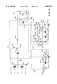
- FIG. 1 describes an electronic ballast with an inverter protection circuit, in accordance with the present invention.
- FIG. 2 describes an inverter control circuit, in accordance with a preferred embodiment of the present invention.
- FIG. 3 describes a high-voltage detection circuit and a no-load detection circuit, in accordance with one embodiment of the present invention.
- FIG. 4 describes a high-voltage detection circuit and a no-load detection circuit for use in an electronic ballast for powering one gas discharge lamp, in accordance with a preferred embodiment of the present invention.
- FIG. 5 describes an AC-to-DC converter, a startup circuit, and a bootstrap circuit for use in the ballast illustrated in FIG. 1, in accordance with a preferred embodiment of the present invention.
- FIG. 6 describes a high-voltage detection circuit and a no-load detection circuit for use in an electronic ballast for powering two gas discharge lamps, in accordance with a preferred embodiment of the present invention.
- Ballast 10 for powering a gas discharge lamp 20 is described in FIG. 1.
- Ballast 10 comprises an alternating current (AC) to direct current (DC) converter 100, an inverter 200, an output circuit 400, a high-voltage detection circuit 500, an a no-load detection circuit 600.
- AC alternating current
- DC direct current
- AC-to-DC converter 100 includes a pair of input connections 102,104 for receiving a source of alternating current 50, and a pair of output connections 106,108.
- Inverter 200 comprises first and second input terminals 202,204, an output terminal 206, a first inverter switch 210, a second inverter switch 220, an inverter control circuit 300, a startup circuit 240, and a bootstrap circuit 260.
- First and second input terminals 202,204 are coupled to the output connections 106,108 of AC-to-DC converter 100.
- Second input terminal 204 is also coupled to a circuit ground node 60.
- Inverter switches 210,220 may be implemented using any of a number of controllable power switching devices, such as field-effect transistors (shown in FIG.
- Inverter control circuit 300 includes a DC supply input 302 for receiving operating power, a first drive output 308 coupled to first inverter switch 210, a second drive output 312 coupled to second inverter switch 220, a high-voltage detect (HVD) input 304, and a no-load detect (NLD) input 306.
- inverter control circuit 300 also includes an auxiliary output 310 coupled to the junction of inverter switches 210,220 at inverter output terminal 206.
- Startup circuit 240 coupled between AC-to-DC converter 100 and DC supply input 302, is operable to provide power for initiating operation of inverter control circuit 300 following initial application of AC power to ballast 10.
- Bootstrap circuit 260 coupled between inverter output terminal 206 and DC supply input 302, provide steady-state operating power to inverter control circuit 300.
- output circuit 400 comprises a set of output wires 402,404,406,408, a direct current (DC) blocking capacitor 420, a direct current (DC) path resistor 424, a resonant inductor 430, and a resonant capacitor 440.
- Output wires 402,404,406,408 are adapted to being coupled to a gas discharge lamp 20. More specifically, first output wire 402 is coupleable to second output wire 404 through a first filament 22 of lamp 20, while third output wire 406 is coupleable to fourth output wire 408 through a second filament 24 of lamp 20.
- DC blocking capacitor 420 is coupled between inverter output terminal 206 and a first node 422.
- DC path resistor 424 is coupled between first input terminal 202 of inverter 200 and first node 422.
- the function of DC path resistor 424 is to provide a circuit path whereby a DC current is allowed to flow even when inverter 200 is off. As will be explained below, this DC current plays an important part in allowing ballast 10 to automatically ignite and operate a replaced lamp.
- Resonant inductor 430 is coupled between first node 422 and first output wire 402.
- Resonant capacitor 440 is coupled between second output wire 404 and third output wire 406.
- Output circuit 400 is configured as a series resonant circuit that provides a high voltage for igniting lamp 20 and a magnitude-limited current for steady-state powering of lamp 20.
- output circuit 400 is commonly referred to as a "direct-coupled" arrangement, in that physical disconnection of lamp 20 from output wires 402, . . . ,408, or failure of either of the lamp filaments 22,24, effectively disconnects resonant capacitor 440 from the rest of output circuit 400.
- This type of output wire arrangement is common in electronic ballasts used in a number of European countries.
- high-voltage detection circuit 500 is coupled between second output wire 404 and HVD input 304 of inverter control circuit 300.
- No-load detection circuit 600 is coupled between fourth output wire 408 and NLD input 306 of inverter control circuit 300.
- high-voltage detection circuit 500 and no-load detection circuit 600 monitor lamp 20 and convey information regarding operation of lamp 20 to inverter control circuit 300. This information includes whether or not lamp 20 is indeed present and properly connected to output wires 402, . . . ,408, and whether or not lamp 20 is operating in a normal manner.
- inverter control circuit 300 is operable to: (1) provide an ignition period following initial application of electrical power to ballast 10, wherein, regardless of the signals applied to the HVD and NLD inputs 304,306, inverter switches 210,220 are switched on and off in a complementary fashion (i.e., inverter switch 210 is on while inverter switch 220 is off, and vice-versa) for at least a first predetermined period of time; (2) continue to provide complementary switching of inverter switches 210,220 as long as lamp 20 is operating normally; (3) terminate switching of inverter switches 210,220 in response to various lamp-fault conditions; and (4) provide a relamping period wherein complementary switching of inverter switches 210,220 is automatically resumed for at least a second predetermined period of time following replacement of a defective or failed lamp with a new lamp.
- the various lamp-fault conditions that cause inverter control circuit 300 to terminate switching of inverter switches 210,220 include: (i) failure of lamp 20 to ignite and operate normally within the ignition period; (ii) removal (i.e., physical disconnection) of lamp 20; (iii) failure of lamp 20 to conduct current in a substantially normal fashion (such as what occurs with a degassed or diode-mode lamp); and (iv) opening of either one or both filaments 22,24 of lamp 20. Additionally, inverter control circuit 300 terminates switching of inverter switches 210,220 when, following replacement of a failed lamp with a new lamp, the new lamp fails to ignite and operate normally within the relamping period.
- inverter control circuit 300 further includes a driver circuit 320, an internal reference source 350 for providing a reference voltage 356 (V REF ), a first comparator 330, a second comparator 340, and a protection logic circuit 360.
- V REF reference voltage 356
- Driver circuit 320 is coupled to first and second drive outputs 308,312, and includes a shutdown input 322. As shown previously with regard to FIG. 1, first and second drive outputs 308,312 are coupled to inverter switches 210,220. If inverter switches 210,220 are to be used in a half-bridge type inverter, driver circuit 320 is further coupled to auxiliary output 310. During operation, driver circuit 320 provides complementary switching of inverter switches 210,220 when a logic "0" is applied to shutdown input 322, and terminates switching of inverter switches 210,220 when a logic "1" is applied to shutdown input 322. Driver circuit 320 may be implemented using circuitry like that which is employed in existing high-side driver devices, such as the IR2151 high-side driver integrated circuit manufactured by International Rectifier.
- First comparator 330 has a non-inverting input 332 coupled to HVD input 304, an inverting input 334 coupled to internal reference source 350, and an HVD output 336.
- First comparator 330 provides a logic "1" at HVD output 336 when the voltage at HVD input 304 exceeds the reference voltage, V REF , and a logic "0" at HVD output 336 when the voltage at HVD input 304 is less than V REF .
- Second comparator 340 has an inverting input 342 coupled to NLD input 306, a non-inverting input 344 coupled to internal reference source 350, and an NLD output 346.
- Second comparator 340 provides a logic "0" at NLD output 346 when the voltage at NLD input 306 exceeds V REF , and a logic “1" at NLD output 346 when the voltage at NLD input 306 is less than V REF .
- Protection logic circuit 360 which is preferably realized using conventional logic gates and flip-flops, receives HVD and NLD outputs 336,346 from comparators 330,340 and provides a shutdown signal 362 to the shutdown input 322 of driver circuit 320. More specifically, protection logic circuit 360 operates in such a way that shutdown signal 362 is a logic "0" for each of the following conditions: (1) during the ignition period following initial application of power to ballast 10; (2) when HVD output 336 is a logic "0” and NLD output 346 is a logic "0”; and (3) when NLD output 346 is a logic "1” and HVD output 336 changes from a logic "0" to a logic "1".
- shutdown signal 362 is a logic "1" for each of the following conditions: (1) when HVD output 336 is a logic “1” (regardless of the value of NLD output 346); and (2) when NLD output 346 is a logic “1” and HVD output 336 is not changing from a logic "0" to a logic “1".
- driver circuit 320 is allowed to continue providing complementary switching of inverter switches 210,220.
- driver circuit 320 ceases to provide complementary switching of inverter switches 210,220 and inverter 200 is thus effectively turned off.
- internal reference source 350 provides a reference voltage, V REF , that is preferably adjusted in dependence on shutdown signal 362.
- V REF is at a first level (e.g., 0.6 volts) when shutdown signal 362 is a logic "0", and at a second level (e.g., 0.3 volts) when shutdown signal 362 is a logic "1".
- V REF adjustable based on the value of shutdown signal 362 facilitates relamping in a ballast for powering two or more lamps.
- inverter control circuit 300 Since driver circuit 320, first and second comparators 330,340, internal reference source 350, and protection logic circuit 360 are all relatively low-power circuits, inverter control circuit 300 is very well-suited for implementation as a single integrated circuit. Advantageously, since a considerable portion of the protection circuitry is incorporated within inverter control circuit 300, the number of discrete components in high-voltage detection circuit 500 and no-load detection circuit 600 can be greatly reduced. This results in a lower component count that significantly enhances the reliability and manufacturability of ballast 10.
- high-voltage detection circuit 500 comprises a first resistor 502, a second resistor 506, a third resistor 510, a first diode 512, a first capacitor 518, and a fourth resistor 520.
- First resistor 502 is coupled between second output wire 404 and a second node 504.
- Second resistor 506 is coupled between second node 504 and a third node 508.
- first and second resistors 502,506 may be replaced by a single resistor.
- Third resistor 510 is coupled between third node 508 and circuit ground node 60.
- First diode 512 has an anode 514 coupled to coupled to third node 508 and a cathode 516 coupled to HVD input 304 of inverter control circuit 300.
- First capacitor 518 and fourth resistor 520 are each coupled between HVD input 304 and circuit ground node 60.
- high-voltage detection circuit 500 monitors the voltage, V OUT , at second output wire 404 and provides a voltage at HVD input 304 that is substantially proportional to the peak value of the positive half cycles of V OUT .
- Resistors 502,506,510 function as a voltage divider for transferring a fractional portion of V OUT into first capacitor 518 via first diode 512.
- First diode 512 serves as a peak-detecting rectifier that allows capacitor 518 to charge up during the positive half cycles of V OUT and prevents capacitor 518 from discharging during the negative half cycles of V OUT .
- Resistor 520 serves as a reset resistor for discharging capacitor 518 so that, following correction of a lamp fault condition, the voltage at HVD input 304 returns to a lower value reflective of the fact that V OUT has returned to a lower, normal value.
- V OUT When lamp 20 is operating normally, V OUT is relatively low so the voltage at HVD input 304 will be correspondingly low (i.e., a logic "0"). That is, high-voltage detection circuit 500 provides a logic "0" at HVD input 304 in response to each of the following conditions: (i) when lamp 20 is conducting current in a substantially normal fashion; (ii) when lamp 20 is removed; and (iii) when at least one of the lamp filaments 22,24 is open. On the other hand, if lamp 20 begins to operate in a substantially abnormal fashion, V OUT becomes considerably higher than normal; note that, because output circuit 400 is direct-coupled, both lamp filaments 22,24 must be intact and properly connected to output wires 402, . . .
- high-voltage detection circuit 500 provides a logic "1" at HVD input 304 of inverter control circuit 300 in response to failure of lamp 20 to conduct current in a substantially normal fashion while both of its filaments 22,24 are intact.
- high-voltage detection circuit 500 is operable to detect a positive overvoltage condition at second output wire 404
- high-voltage detection circuit 500' includes additional circuitry for detecting both positive and negative overvoltage conditions at second output wire 404. Since a diode-mode lamp may cause either positive or negative overvoltage conditions at second output wire 404, high-voltage detection circuit 500' thus provides more complete and reliable detection of diode-mode behavior in lamp 20.
- the additional circuitry includes a second diode 522, a second capacitor 530, an electronic switch 540, a fifth resistor 548, a first zener diode 532, and a sixth resistor 550.
- Second diode 522 has a cathode 526 coupled to second node 504 and an anode 524 coupled to a fourth node 528.
- Second capacitor 530 is coupled between fourth node 528 and circuit ground node 60.
- Electronic switch 540 which is preferably implemented as a PNP-type bipolar junction transistor, has an emitter lead 542 coupled to DC supply input 302 of inverter control circuit 300, a collector lead 546, and a base lead 544.
- Fifth resistor 548 is coupled between base lead 544 and emitter lead 542.
- First zener diode 532 has an anode 534 coupled to fourth node 528, and a cathode 536 coupled to base lead 544.
- Sixth resistor 550 is coupled between collector lead 546 and HVD input 304 of inverter control circuit 300.
- resistors 502,506,510 serve as a voltage divider.
- capacitor 518 takes on a voltage that is roughly proportional to the peak value of the positive half cycles of V OUT .
- Capacitor 530 and diode 522 serve a similar function with regard to the negative half cycles of V OUT . That is, capacitor 530 takes on a negative voltage (i.e., with a polarity such that node 528 is at a lower potential than circuit ground node 60) that is representative of the peak value of the negative half cycles of V OUT .
- zener diode 532 As long as the negative voltage across capacitor 530 is less than the zener voltage, V z , of zener diode 532, zener diode 532 remains non-conductive and transistor 540 remains off. On the other hand, if V OUT becomes sufficiently large, the voltage across capacitor 530 will become large enough to attempt to exceed V z . When this occurs, zener diode 532 turns on and begins to conduct a positive current from cathode 536 to anode 534. This turns on transistor 540, which then couples the DC voltage (e.g. 15 volts) at DC supply input 302 to HVD input 304, thus providing a voltage at HVD input 304 that amounts to a logic "1". In this way, high-voltage detection circuit 500' monitors output circuit 400 for both negative and positive overvoltage conditions.
- DC voltage e.g. 15 volts
- no-load detection circuit 600 comprises a seventh resistor 602, a third diode 604, a third capacitor 610, and an eighth resistor 612. Seventh resistor 602 is coupled between fourth output wire 408 and circuit ground node 60.
- Third diode 604 has an anode 606 coupled to fourth output wire 408 and a cathode 608 coupled to NLD input 306 of inverter control circuit 300.
- Third capacitor 610 and eighth resistor 612 are each coupled between NLD input 306 and circuit ground node 60.
- no-load detection circuit 600 monitors the "return current" flows into fourth output wire 408 as an indicator of whether or not a lamp with both filaments intact is indeed connected to ballast 10.
- Resistor 602 serves as a current sensing resistor and has a voltage that is proportional to the return current.
- Diode 604 and capacitor 610 function as a peak detector in which the voltage provided at NLD input 306 is substantially proportional to the peak value of the positive half-cycles of the return current.
- no-load detection circuit 600 provides a logic "1" at NLD input 306 in response to both lamp filaments 22,24 being intact, and provides a logic "0" at NLD input 306 in response to each of the following conditions: (i) when lamp 20 is removed; and (ii) when at least one of the lamp filaments 22,24 is open.
- no-load detection circuit 600' further includes a fourth diode 620 having an anode 624 coupled to circuit ground node 60 and a cathode coupled to fourth output wire 408.
- Fourth diode 620 reduces the power dissipation in resistor 602 by providing a bypass path around resistor 602 for the negative-going half cycles of the return current. The positive-going half cycles of the return current continue to flow through resistor 602 as previously described.
- AC-to-DC converter 100 preferably comprises a full-wave rectifier circuit 110 coupled between input connections 102,104 and output connections 106,108, and a bulk capacitor 120 coupled across output connections 106,108.
- Rectifier circuit 110 is operable to accept the source of alternating current 50 and to provide a unidirectional voltage between output connections 106,108.
- Bulk capacitor 120 serves as a filtering capacitor for reducing the amount of AC ripple in the output voltage provided by rectifier circuit 110.
- AC-to-DC converter may also include a boost converter (not shown), inserted between rectifier circuit 110 and bulk capacitor 120, for providing power factor correction and line regulation.
- startup circuit 240 preferably comprises a pull-down resistor 242 coupled between DC supply input 302 and the first output connection 106 of AC-to-DC converter 100, and a filtering capacitor 244 coupled between DC supply input 302 and circuit ground node 60.
- Bootstrap circuit 260 comprises a fourth capacitor 262, a second zener diode 266, a fifth diode 272, and (optionally) a current-limiting resistor 278.
- Fourth capacitor 262 is coupled between inverter output terminal 206 and a fifth node 264, and serves as an AC coupling capacitor for extracting a limited amount of current from inverter output terminal 206.
- Second zener diode 266 which functions as a voltage regulator that safely limits the amount of voltage provided to DC supply input 302, has a cathode 270 coupled to fifth node 264 and an anode coupled to circuit ground node 60.
- Fifth diode 272 which serves as a rectifier for transferring only positive-going current to DC supply input 302, has an anode 274 coupled to fifth node 264 and a cathode 276 coupled (either directly or via currentlimiting resistor 278) to DC supply input 302.
- capacitor 244 When AC power is first applied to the ballast, capacitor 244 is initially uncharged, and inverter control circuit 300 is off and remains off until such time as the voltage at DC supply input 302 reaches a certain level. With AC power applied to the ballast, AC-to-DC converter 100 provides a substantially DC voltage across output connections 106,108, and capacitor 244 begins to charge up due to current delivered to it via resistor 242. Once the voltage across capacitor 244 reaches a certain predetermined level (e.g. 10 volts), inverter control circuit 300 turns on and, using the energy stored in capacitor 244, begins switching of inverter switches 210,220. At this point, the energy stored in capacitor 244 begins to be depleted.
- a certain predetermined level e.g. 10 volts
- bootstrap circuit 260 begins to operate and provides the steady-state power needed to keep inverter control circuit 300 operating.
- Capacitor 244 additionally serves as a filtering capacitor for storing energy provided by bootstrap circuit 260.
- startup circuit 240 provides a relatively small amount of energy for initially activating inverter control circuit 300, while bootstrap circuit 260 supplies steady-state power for sustaining operation of inverter control circuit 300.
- output circuit 400' additionally includes a second resonant inductor 432, a second resonant capacitor 442, and a second set of output wires 410,412,414,416 adapted to being coupled to a second gas discharge lamp 30.
- Second resonant inductor 432 is coupled between first node 422 and a fifth output wire 410.
- Second resonant capacitor 442 is coupled between a sixth output wire 412 and a seventh output wire 414.
- Fifth output wire 410 is coupleable to sixth output wire 412 through a first filament 32 of lamp 30, while seventh output wire 414 is coupleable to eighth output wire 416 through a second filament 34 of lamp 30.
- Eighth output wire 416 is also coupled to fourth output wire 408.
- high-voltage detection circuit 500" additionally includes a ninth resistor 560 coupled between sixth output wire 412 and second node 504.
- Ninth resistor 560 is analogous in function to resistor 502 and allows high-voltage detection circuit 500" to monitor for overvoltage due to second lamp 30 becoming degassed or operating in the diode mode.
- high-voltage detection circuit 500" is operable to provide a logic "1" at HVD input 304 in response to failure of either one or both of the lamps 20,30 to conduct current in a substantially normal fashion while both of its lamp filaments are intact.
- high-voltage detection circuit 500" will provide a logic "0" at HVD input 304 in response to each of the following conditions: (1) both lamps conducting current in a substantially normal fashion; (2) removal of both lamps; (3) both lamps having at least one open filament; and (4) each failed lamp (if any) having at least one open filament.
- no-load detection circuit 600' provides a logic "1" at NLD input 306 as long as the inverter is operating and at least one of the lamps has both of its filaments intact. Conversely, in order for no-load detection circuit 600' to provide a logic "0" at NLD input 306, both lamps must be removed or each lamp must have at least one open filament.
- inverter control circuit 300 will continue to provide switching of the inverter switches since removal of lamp 20 presents no danger to continued safe operation of the inverter as long as lamp 30 continues to operate normally.
- either lamp fails to conduct current in a normal manner, but both of its filaments remain intact (i.e., such as what may occur with a degassed or diode-mode lamp)
- no-load detection circuit 600' will provide a logic "1" at NLD input 306.
- ballast 10 provides a high degree of protection for the inverter under a number of lamp failure modes, yet accommodates "parallel” operation by which the remaining "good” lamp is allowed to continue to operate, and thus provide useful illumination, if the "problem” lamps are either (1) removed; or (2) failed, with at least one filament.
- ballast 10 under various lamp fault conditions is now explained with reference to FIGS. 2 and 6 as follows.
- HVD input 304 When both lamps 20,30 are present and operating normally with their filaments intact, a logic "0" is provided at HVD input 304 and a logic “1" is provided at NLD input 306. Stated differently, the voltage at HVD input 304 is low (e.g., 0.4 volts) and the voltage at NLD input 306 is high (e.g., 2.4 volts). During this time, since shutdown signal 362 is a logic "0”the reference voltage V REF provided by internal reference source 350 is at its first level (e.g., 0.6 volts). Thus, HVD output 336 is a logic “0” and NLD output 346 is a logic “0”, so shutdown signal 362 remains a logic "0” and driver circuit 320 continues to provide complementary switching of inverter switches 210,220.
- capacitor 440 is disconnected from the rest of output circuit 400. Consequently, the voltage at HVD input 304 remains low, and actually decreases (e.g., to 0.2 volts) since current is no longer supplied to high-voltage detection circuit 500 via resistor 502.
- the voltage at NLD input 306 similarly decreases (e.g., to 1.2 volts) since the return current is now about half of what it was when both lamps 20,30 were present and operating.
- ballast 10 provides so-called "parallel" operation of two or more lamps.
- HVD input 304 again remains low due to no current being provided to high voltage detection circuit 500". Since the return current is now zero, NLD input 306 goes to zero. Consequently, NLD output 346 from comparator 340 becomes a logic "1" and, in response, protection logic circuit 360 causes shutdown signal 362 to become a logic "1". This turns off driver circuit 320, thereby terminating switching of inverter switches 210,220. With shutdown signal 362 now a logic "1", internal reference source 350 changes V REF from its first level (e.g., 0.6 volts) to its second level (e.g., 0.3 volts), where it remains as long as shutdown signal 362 is a logic "1".
- first level e.g., 0.6 volts
- second level e.g., 0.3 volts
- HVD output 336 of comparator 330 goes to a logic "1"; note that this would not be the case if V REF had been allowed to remain at its first level (e.g., 0.6 volts), in which case HVD output 336 would remain a logic "0".
- protection logic circuit 360 in response to HVD output 336 changing from a logic "0" to a logic "1" while NLD output is a logic "1", protection logic circuit 360 then changes shutdown signal 362 to a logic "0".
- ballast 10 provides for automatic ignition and operation of a replaced lamp following shutdown of the inverter due to a lamp fault condition.
- inverter control circuit 300 terminates inverter switching, even though the remaining lamp may be "good". This is necessary in order to protect the ballast from otherwise certain damage arising from overvoltage in output circuit 400'. In this case, the defective lamp (e.g., lamp 30) must be removed and replaced with an operational lamp in order for inverter protection circuit 300 to resume inverter switching.
- each of the lamps 20,30 develops at least one open filament (e.g., filaments 22,34 become open), no return current is provided to no-load detection circuit 600'. Consequently, the voltage at NLD input 306 goes to zero. Because each lamp 20,30 has at least one open filament. resonant capacitors 440,442 are effectively disconnected from the rest of output circuit 400', so no harmful overvoltage condition can develop in output circuit 400'. Nevertheless, inverter control circuit 300 responds to this no-load condition by terminating inverter switching, thus preventing needless power dissipation in inverter switches 210,220.
- inverter control circuit 300 responds to this no-load condition by terminating inverter switching, thus preventing needless power dissipation in inverter switches 210,220.
Abstract
Description
Claims (31)
Priority Applications (1)
| Application Number | Priority Date | Filing Date | Title |
|---|---|---|---|
| US08/984,444 US5883473A (en) | 1997-12-03 | 1997-12-03 | Electronic Ballast with inverter protection circuit |
Applications Claiming Priority (1)
| Application Number | Priority Date | Filing Date | Title |
|---|---|---|---|
| US08/984,444 US5883473A (en) | 1997-12-03 | 1997-12-03 | Electronic Ballast with inverter protection circuit |
Publications (1)
| Publication Number | Publication Date |
|---|---|
| US5883473A true US5883473A (en) | 1999-03-16 |
Family
ID=25530556
Family Applications (1)
| Application Number | Title | Priority Date | Filing Date |
|---|---|---|---|
| US08/984,444 Expired - Lifetime US5883473A (en) | 1997-12-03 | 1997-12-03 | Electronic Ballast with inverter protection circuit |
Country Status (1)
| Country | Link |
|---|---|
| US (1) | US5883473A (en) |
Cited By (71)
| Publication number | Priority date | Publication date | Assignee | Title |
|---|---|---|---|---|
| US5945788A (en) * | 1998-03-30 | 1999-08-31 | Motorola Inc. | Electronic ballast with inverter control circuit |
| WO2000069226A1 (en) * | 1999-05-06 | 2000-11-16 | Koninklijke Philips Electronics N.V. | Circuit arrangement |
| US6175189B1 (en) * | 1999-04-06 | 2001-01-16 | Bruce Industries, Inc. | Floating reference fault protection circuit for arc discharge lamp ballast |
| US6232727B1 (en) * | 1998-10-07 | 2001-05-15 | Micro Linear Corporation | Controlling gas discharge lamp intensity with power regulation and end of life protection |
| US6252357B1 (en) * | 1998-03-31 | 2001-06-26 | Toshiba Lighting & Technology Corporation | Self-ballasted fluorescent lamp and lighting fixture |
| US6331755B1 (en) * | 1998-01-13 | 2001-12-18 | International Rectifier Corporation | Circuit for detecting near or below resonance operation of a fluorescent lamp driven by half-bridge circuit |
| US6407593B1 (en) * | 1999-06-30 | 2002-06-18 | Denso Corporation | Electromagnetic load control apparatus having variable drive-starting energy supply |
| US6429603B1 (en) * | 1999-04-28 | 2002-08-06 | Mitsubishi Denki Kabushiki Kaisha | Discharge lamp lighting apparatus |
| WO2002078405A2 (en) * | 2001-03-27 | 2002-10-03 | Koninklijke Philips Electronics N.V. | Panic protection from fault conditions in power converters |
| US20030031037A1 (en) * | 2001-07-02 | 2003-02-13 | The Delta Group | Converter for converting an AC power main voltage to a voltage suitable for driving a lamp |
| EP1286574A1 (en) * | 2001-08-06 | 2003-02-26 | Osram-Sylvania Inc. | Ballast with efficient filament preheating and lamp fault detection |
| WO2003019993A1 (en) * | 2001-08-27 | 2003-03-06 | Koninklijke Philips Electronics N.V. | Circuit arrangement |
| DE10206731A1 (en) * | 2002-02-18 | 2003-08-28 | Tridonicatco Gmbh & Co Kg | Lamp sensor for a ballast for operating a gas discharge lamp |
| US6633139B2 (en) * | 2001-07-02 | 2003-10-14 | Groupe Delta Xfo, Inc. | Converter for converting an AC power main voltage to a voltage suitable for driving a lamp |
| US20040051476A1 (en) * | 2002-08-28 | 2004-03-18 | Minebea Co., Ltd. | Discharge lamp lighting circuit with protection circuit |
| US6710551B2 (en) * | 2001-03-02 | 2004-03-23 | Toshiba Lighting & Technology Corporation | High-intensity discharge lamp lighting apparatus and luminaire for using the same |
| US6720739B2 (en) * | 2001-09-17 | 2004-04-13 | Osram Sylvania, Inc. | Ballast with protection circuit for quickly responding to electrical disturbances |
| US20040124785A1 (en) * | 2000-07-21 | 2004-07-01 | Alexandrov Felix I. | Method and apparatus for arc detection and protection for electronic ballasts |
| US20040189216A1 (en) * | 2003-03-26 | 2004-09-30 | Hwangsoo Choi | Shorted lamp detection in backlight system |
| US20050190142A1 (en) * | 2004-02-09 | 2005-09-01 | Ferguson Bruce R. | Method and apparatus to control display brightness with ambient light correction |
| US20050195626A1 (en) * | 2004-02-19 | 2005-09-08 | International Rectifier Corporation | Pendulum resonant converter and method |
| US7042161B1 (en) | 2005-02-28 | 2006-05-09 | Osram Sylvania, Inc. | Ballast with arc protection circuit |
| US20060098363A1 (en) * | 2004-11-09 | 2006-05-11 | Fultec Semiconductors, Inc. | Integrated transient blocking unit compatible with very high voltages |
| US20060108998A1 (en) * | 2002-11-11 | 2006-05-25 | Van Zundert Roy Hendrik Anna M | Magnetic resonance imaging system with a plurality of transmit coils |
| US20060244394A1 (en) * | 2005-04-29 | 2006-11-02 | Benq Corporation | Inverter capable of switching working frequency |
| EP1736037A2 (en) * | 2004-04-08 | 2006-12-27 | International Rectifier Corporation | Pfc and ballast control ic |
| US20070014130A1 (en) * | 2004-04-01 | 2007-01-18 | Chii-Fa Chiou | Full-bridge and half-bridge compatible driver timing schedule for direct drive backlight system |
| US20070042729A1 (en) * | 2005-08-16 | 2007-02-22 | Baaman David W | Inductive power supply, remote device powered by inductive power supply and method for operating same |
| US7183714B1 (en) | 2005-06-30 | 2007-02-27 | Osram Sylvania, Inc. | Ballast with relamping circuitry |
| WO2007025849A1 (en) * | 2005-08-30 | 2007-03-08 | Patent-Treuhand-Gesellschaft F�R Elektrische Gl�Hlampen Mbh | Circuit arrangement and method for operating at least one electric lamp |
| US20070132398A1 (en) * | 2003-09-23 | 2007-06-14 | Microsemi Corporation | Optical and temperature feedbacks to control display brightness |
| WO2007105748A1 (en) * | 2006-03-07 | 2007-09-20 | Matsushita Electric Works, Ltd. | Discharge lamp lighting device, lighting system and method |
| US7288901B1 (en) | 2006-09-15 | 2007-10-30 | Osram Sylvania Inc. | Ballast with arc protection circuit |
| US7312588B1 (en) | 2006-09-15 | 2007-12-25 | Osram Sylvania, Inc. | Ballast with frequency-diagnostic lamp fault protection circuit |
| US20070296416A1 (en) * | 2006-05-30 | 2007-12-27 | Lee Young-Sik | Circuit for detecting end of life of fluorescent lamp |
| US20080024075A1 (en) * | 2002-12-13 | 2008-01-31 | Microsemi Corporation | Apparatus and method for striking a fluorescent lamp |
| US7382636B2 (en) | 2005-10-14 | 2008-06-03 | Access Business Group International Llc | System and method for powering a load |
| WO2008138391A1 (en) * | 2007-05-10 | 2008-11-20 | Osram Gesellschaft mit beschränkter Haftung | Circuit arrangement and method for the operation of at least one discharge lamp |
| US20090024143A1 (en) * | 2007-07-18 | 2009-01-22 | Crews Samuel T | Endoscopic implant system and method |
| US20090121639A1 (en) * | 2005-05-04 | 2009-05-14 | Stmicroelectronics S.R.L. | Control device for discharge lamp |
| WO2009062552A1 (en) * | 2007-11-15 | 2009-05-22 | Osram Gesellschaft mit beschränkter Haftung | Apparatus and method for testing of wiring for at least one discharge lamp |
| US20090200951A1 (en) * | 2008-02-08 | 2009-08-13 | Purespectrum, Inc. | Methods and Apparatus for Dimming Light Sources |
| US20090200953A1 (en) * | 2008-02-08 | 2009-08-13 | Ray James King | Methods and apparatus for a high power factor ballast having high efficiency during normal operation and during dimming |
| US20090200960A1 (en) * | 2008-02-08 | 2009-08-13 | Pure Spectrum, Inc. | Methods and Apparatus for Self-Starting Dimmable Ballasts With A High Power Factor |
| US20090200952A1 (en) * | 2008-02-08 | 2009-08-13 | Purespectrum, Inc. | Methods and apparatus for dimming light sources |
| US20090200965A1 (en) * | 2008-02-08 | 2009-08-13 | Purespectrum, Inc. | Energy savings circuitry for a lighting ballast |
| US20090200964A1 (en) * | 2008-02-08 | 2009-08-13 | King Ray J | Methods And Apparatus For Dimmable Ballasts With A High Power Factor |
| US20090206767A1 (en) * | 2003-09-09 | 2009-08-20 | Microsemi Corporation | Split phase inverters for ccfl backlight system |
| US20090273295A1 (en) * | 2006-07-06 | 2009-11-05 | Microsemi Corporation | Striking and open lamp regulation for ccfl controller |
| US20090295300A1 (en) * | 2008-02-08 | 2009-12-03 | Purespectrum, Inc | Methods and apparatus for a dimmable ballast for use with led based light sources |
| WO2009147562A2 (en) * | 2008-06-06 | 2009-12-10 | Koninklijke Philips Electronics, N.V. | Electronic ballast and fault protection method |
| US20100134091A1 (en) * | 2008-11-28 | 2010-06-03 | Eom Hyun-Chul | Abnormal switching monitoring device and abnormal switching monitoring method |
| US7755595B2 (en) | 2004-06-07 | 2010-07-13 | Microsemi Corporation | Dual-slope brightness control for transflective displays |
| US20100176733A1 (en) * | 2009-01-14 | 2010-07-15 | Purespectrum, Inc. | Automated Dimming Methods and Systems For Lighting |
| US7768755B1 (en) | 2007-12-04 | 2010-08-03 | Universal Lighting Technologies, Inc. | Over-voltage protection and automatic re-strike circuit for an electronic ballast |
| US20100213944A1 (en) * | 2009-02-25 | 2010-08-26 | Gye Hyun Cho | Diagnosis Device, Diagnosis Method, And Lamp Ballast Circuit Using The Same |
| DE10196562B4 (en) * | 2000-09-06 | 2010-09-09 | Panasonic Electric Works Co., Ltd., Kadoma-shi | Ballast for the operation of a discharge lamp |
| US20100225239A1 (en) * | 2009-03-04 | 2010-09-09 | Purespectrum, Inc. | Methods and apparatus for a high power factor, high efficiency, dimmable, rapid starting cold cathode lighting ballast |
| US20110187271A1 (en) * | 2010-02-01 | 2011-08-04 | Twisthink, L.L.C. | Luminary control systems |
| WO2011107902A3 (en) * | 2010-03-01 | 2011-12-08 | Koninklijke Philips Electronics N.V. | Fluorescent lamp information detection system and method |
| US8093839B2 (en) | 2008-11-20 | 2012-01-10 | Microsemi Corporation | Method and apparatus for driving CCFL at low burst duty cycle rates |
| EP2557901A1 (en) * | 2011-08-08 | 2013-02-13 | Skynet Electronic Co., Ltd. | Electronic ballast capable of self-protection at natural or premature end of life of fluorescent light tube |
| US8482213B1 (en) | 2009-06-29 | 2013-07-09 | Panasonic Corporation | Electronic ballast with pulse detection circuit for lamp end of life and output short protection |
| WO2013151641A1 (en) * | 2012-04-03 | 2013-10-10 | General Electric Company | Relamping circuit for fluorescent ballasts |
| US8564216B1 (en) * | 2011-02-02 | 2013-10-22 | Universal Lighting Technologies, Inc. | Asymmetric end-of-life protection circuit for fluorescent lamp ballasts |
| US8947020B1 (en) | 2011-11-17 | 2015-02-03 | Universal Lighting Technologies, Inc. | End of life control for parallel lamp ballast |
| US20150043246A1 (en) * | 2013-08-09 | 2015-02-12 | Osram Sylvania Inc. | Primary side no load detection and shutdown circuit in an isolated driver |
| US20150195894A1 (en) * | 2012-07-17 | 2015-07-09 | General Electric Company | Relamping circuit |
| US20160097575A1 (en) * | 2013-03-01 | 2016-04-07 | Regal Beloit America, Inc. | Motor assembly with integrated on/off detection with speed profile operation |
| US20180254695A1 (en) * | 2015-09-02 | 2018-09-06 | Autonetworks Technologies, Ltd. | Dc-dc converter |
| US10348187B2 (en) * | 2015-12-25 | 2019-07-09 | Autonetworks Technologies, Ltd. | DC-DC converter having a reverse flow protection function |
Citations (4)
| Publication number | Priority date | Publication date | Assignee | Title |
|---|---|---|---|---|
| US5089753A (en) * | 1990-07-09 | 1992-02-18 | North American Philips Corporation | Arrangement for predicting failure in fluorescent lamp systems |
| US5140229A (en) * | 1990-04-28 | 1992-08-18 | Koito Manufacturing Co., Ltd. | Lighting circuit for vehicular discharge lamp |
| US5650694A (en) * | 1995-03-31 | 1997-07-22 | Philips Electronics North America Corporation | Lamp controller with lamp status detection and safety circuitry |
| US5739645A (en) * | 1996-05-10 | 1998-04-14 | Philips Electronics North America Corporation | Electronic ballast with lamp flash protection circuit |
-
1997
- 1997-12-03 US US08/984,444 patent/US5883473A/en not_active Expired - Lifetime
Patent Citations (4)
| Publication number | Priority date | Publication date | Assignee | Title |
|---|---|---|---|---|
| US5140229A (en) * | 1990-04-28 | 1992-08-18 | Koito Manufacturing Co., Ltd. | Lighting circuit for vehicular discharge lamp |
| US5089753A (en) * | 1990-07-09 | 1992-02-18 | North American Philips Corporation | Arrangement for predicting failure in fluorescent lamp systems |
| US5650694A (en) * | 1995-03-31 | 1997-07-22 | Philips Electronics North America Corporation | Lamp controller with lamp status detection and safety circuitry |
| US5739645A (en) * | 1996-05-10 | 1998-04-14 | Philips Electronics North America Corporation | Electronic ballast with lamp flash protection circuit |
Cited By (111)
| Publication number | Priority date | Publication date | Assignee | Title |
|---|---|---|---|---|
| US6331755B1 (en) * | 1998-01-13 | 2001-12-18 | International Rectifier Corporation | Circuit for detecting near or below resonance operation of a fluorescent lamp driven by half-bridge circuit |
| US5945788A (en) * | 1998-03-30 | 1999-08-31 | Motorola Inc. | Electronic ballast with inverter control circuit |
| US6252357B1 (en) * | 1998-03-31 | 2001-06-26 | Toshiba Lighting & Technology Corporation | Self-ballasted fluorescent lamp and lighting fixture |
| US6232727B1 (en) * | 1998-10-07 | 2001-05-15 | Micro Linear Corporation | Controlling gas discharge lamp intensity with power regulation and end of life protection |
| US6175189B1 (en) * | 1999-04-06 | 2001-01-16 | Bruce Industries, Inc. | Floating reference fault protection circuit for arc discharge lamp ballast |
| US6429603B1 (en) * | 1999-04-28 | 2002-08-06 | Mitsubishi Denki Kabushiki Kaisha | Discharge lamp lighting apparatus |
| US6307329B1 (en) * | 1999-05-06 | 2001-10-23 | U.S. Philips Corporation | Circuit arrangement |
| WO2000069226A1 (en) * | 1999-05-06 | 2000-11-16 | Koninklijke Philips Electronics N.V. | Circuit arrangement |
| US6407593B1 (en) * | 1999-06-30 | 2002-06-18 | Denso Corporation | Electromagnetic load control apparatus having variable drive-starting energy supply |
| US6809483B2 (en) | 2000-07-21 | 2004-10-26 | Osram Sylvania Inc. | Method and apparatus for arc detection and protection for electronic ballasts |
| US20040124785A1 (en) * | 2000-07-21 | 2004-07-01 | Alexandrov Felix I. | Method and apparatus for arc detection and protection for electronic ballasts |
| DE10196562B4 (en) * | 2000-09-06 | 2010-09-09 | Panasonic Electric Works Co., Ltd., Kadoma-shi | Ballast for the operation of a discharge lamp |
| US6710551B2 (en) * | 2001-03-02 | 2004-03-23 | Toshiba Lighting & Technology Corporation | High-intensity discharge lamp lighting apparatus and luminaire for using the same |
| US6724602B2 (en) | 2001-03-27 | 2004-04-20 | Koninklijke Philips Electronics N.V. | Panic protection from fault conditions in power converters |
| WO2002078405A2 (en) * | 2001-03-27 | 2002-10-03 | Koninklijke Philips Electronics N.V. | Panic protection from fault conditions in power converters |
| US20020141128A1 (en) * | 2001-03-27 | 2002-10-03 | Koninklijke Philips Electronics N.V. | Panic protection from fault conditions in power converters |
| WO2002078405A3 (en) * | 2001-03-27 | 2002-12-05 | Koninkl Philips Electronics Nv | Panic protection from fault conditions in power converters |
| US20030031037A1 (en) * | 2001-07-02 | 2003-02-13 | The Delta Group | Converter for converting an AC power main voltage to a voltage suitable for driving a lamp |
| US6633139B2 (en) * | 2001-07-02 | 2003-10-14 | Groupe Delta Xfo, Inc. | Converter for converting an AC power main voltage to a voltage suitable for driving a lamp |
| US6856098B2 (en) | 2001-07-02 | 2005-02-15 | Éclairage Contraste | Converter for converting an AC power main voltage to a voltage suitable for driving a lamp |
| EP1286574A1 (en) * | 2001-08-06 | 2003-02-26 | Osram-Sylvania Inc. | Ballast with efficient filament preheating and lamp fault detection |
| US6717370B2 (en) | 2001-08-27 | 2004-04-06 | Koninklijke Philips Electronics N.V. | High speed stop circuit for an electronic ballast |
| WO2003019993A1 (en) * | 2001-08-27 | 2003-03-06 | Koninklijke Philips Electronics N.V. | Circuit arrangement |
| US6720739B2 (en) * | 2001-09-17 | 2004-04-13 | Osram Sylvania, Inc. | Ballast with protection circuit for quickly responding to electrical disturbances |
| EP1945008A1 (en) * | 2002-02-18 | 2008-07-16 | TridonicAtco GmbH & Co. KG | Light sensor for a pre-switching device for operating a gas discharge light |
| DE10206731A1 (en) * | 2002-02-18 | 2003-08-28 | Tridonicatco Gmbh & Co Kg | Lamp sensor for a ballast for operating a gas discharge lamp |
| DE10206731B4 (en) * | 2002-02-18 | 2016-12-22 | Tridonic Gmbh & Co Kg | Lamp sensor for a ballast for operating a gas discharge lamp |
| US20040051476A1 (en) * | 2002-08-28 | 2004-03-18 | Minebea Co., Ltd. | Discharge lamp lighting circuit with protection circuit |
| US6710555B1 (en) * | 2002-08-28 | 2004-03-23 | Minebea Co., Ltd. | Discharge lamp lighting circuit with protection circuit |
| US7525261B2 (en) * | 2002-11-11 | 2009-04-28 | Koninklijke Philips Electronics N.V. | Circuit arrangement for operating a high pressure discharge lamp |
| US20060108998A1 (en) * | 2002-11-11 | 2006-05-25 | Van Zundert Roy Hendrik Anna M | Magnetic resonance imaging system with a plurality of transmit coils |
| US20080024075A1 (en) * | 2002-12-13 | 2008-01-31 | Microsemi Corporation | Apparatus and method for striking a fluorescent lamp |
| US6870330B2 (en) | 2003-03-26 | 2005-03-22 | Microsemi Corporation | Shorted lamp detection in backlight system |
| US20040189216A1 (en) * | 2003-03-26 | 2004-09-30 | Hwangsoo Choi | Shorted lamp detection in backlight system |
| US20090206767A1 (en) * | 2003-09-09 | 2009-08-20 | Microsemi Corporation | Split phase inverters for ccfl backlight system |
| US7952298B2 (en) | 2003-09-09 | 2011-05-31 | Microsemi Corporation | Split phase inverters for CCFL backlight system |
| US20070132398A1 (en) * | 2003-09-23 | 2007-06-14 | Microsemi Corporation | Optical and temperature feedbacks to control display brightness |
| US8223117B2 (en) | 2004-02-09 | 2012-07-17 | Microsemi Corporation | Method and apparatus to control display brightness with ambient light correction |
| US20050190142A1 (en) * | 2004-02-09 | 2005-09-01 | Ferguson Bruce R. | Method and apparatus to control display brightness with ambient light correction |
| US20050195626A1 (en) * | 2004-02-19 | 2005-09-08 | International Rectifier Corporation | Pendulum resonant converter and method |
| US7368879B2 (en) * | 2004-02-19 | 2008-05-06 | International Rectifier Corporation | Pendulum resonant converter and method |
| US20070014130A1 (en) * | 2004-04-01 | 2007-01-18 | Chii-Fa Chiou | Full-bridge and half-bridge compatible driver timing schedule for direct drive backlight system |
| US20100090611A1 (en) * | 2004-04-01 | 2010-04-15 | Microsemi Corporation | Full-bridge and half-bridge compatible driver timing schedule for direct drive backlight system |
| US7646152B2 (en) | 2004-04-01 | 2010-01-12 | Microsemi Corporation | Full-bridge and half-bridge compatible driver timing schedule for direct drive backlight system |
| US7965046B2 (en) | 2004-04-01 | 2011-06-21 | Microsemi Corporation | Full-bridge and half-bridge compatible driver timing schedule for direct drive backlight system |
| EP1736037A4 (en) * | 2004-04-08 | 2009-03-04 | Int Rectifier Corp | Pfc and ballast control ic |
| EP1736037A2 (en) * | 2004-04-08 | 2006-12-27 | International Rectifier Corporation | Pfc and ballast control ic |
| US7755595B2 (en) | 2004-06-07 | 2010-07-13 | Microsemi Corporation | Dual-slope brightness control for transflective displays |
| US20060098363A1 (en) * | 2004-11-09 | 2006-05-11 | Fultec Semiconductors, Inc. | Integrated transient blocking unit compatible with very high voltages |
| US7042161B1 (en) | 2005-02-28 | 2006-05-09 | Osram Sylvania, Inc. | Ballast with arc protection circuit |
| EP1696712A1 (en) * | 2005-02-28 | 2006-08-30 | Osram Sylvania Inc. | Ballast with arc protection circuit |
| US7245091B2 (en) * | 2005-04-29 | 2007-07-17 | Benq Corporation | Inverter capable of switching working frequency |
| US20060244394A1 (en) * | 2005-04-29 | 2006-11-02 | Benq Corporation | Inverter capable of switching working frequency |
| US20090121639A1 (en) * | 2005-05-04 | 2009-05-14 | Stmicroelectronics S.R.L. | Control device for discharge lamp |
| US7902764B2 (en) * | 2005-05-04 | 2011-03-08 | Stmicroelectronics S.R.L. | Control device for discharge lamp |
| US7183714B1 (en) | 2005-06-30 | 2007-02-27 | Osram Sylvania, Inc. | Ballast with relamping circuitry |
| US20070042729A1 (en) * | 2005-08-16 | 2007-02-22 | Baaman David W | Inductive power supply, remote device powered by inductive power supply and method for operating same |
| US20090010028A1 (en) * | 2005-08-16 | 2009-01-08 | Access Business Group International Llc | Inductive power supply, remote device powered by inductive power supply and method for operating same |
| WO2007025849A1 (en) * | 2005-08-30 | 2007-03-08 | Patent-Treuhand-Gesellschaft F�R Elektrische Gl�Hlampen Mbh | Circuit arrangement and method for operating at least one electric lamp |
| US7382636B2 (en) | 2005-10-14 | 2008-06-03 | Access Business Group International Llc | System and method for powering a load |
| CN101385398B (en) * | 2006-03-07 | 2012-09-05 | 松下电器产业株式会社 | Discharge lamp lighting device, lighting system and method |
| WO2007105748A1 (en) * | 2006-03-07 | 2007-09-20 | Matsushita Electric Works, Ltd. | Discharge lamp lighting device, lighting system and method |
| JP2009529208A (en) * | 2006-03-07 | 2009-08-13 | パナソニック電工株式会社 | Discharge lamp lighting device, lighting system, and method thereof |
| US20070296416A1 (en) * | 2006-05-30 | 2007-12-27 | Lee Young-Sik | Circuit for detecting end of life of fluorescent lamp |
| US7486029B2 (en) | 2006-05-30 | 2009-02-03 | Fairchild Korea Semiconductor, Ltd. | Circuit for detecting end of life of fluorescent lamp |
| US8358082B2 (en) | 2006-07-06 | 2013-01-22 | Microsemi Corporation | Striking and open lamp regulation for CCFL controller |
| US20090273295A1 (en) * | 2006-07-06 | 2009-11-05 | Microsemi Corporation | Striking and open lamp regulation for ccfl controller |
| US7288901B1 (en) | 2006-09-15 | 2007-10-30 | Osram Sylvania Inc. | Ballast with arc protection circuit |
| US7312588B1 (en) | 2006-09-15 | 2007-12-25 | Osram Sylvania, Inc. | Ballast with frequency-diagnostic lamp fault protection circuit |
| US8169149B2 (en) | 2007-05-10 | 2012-05-01 | Osram Ag | Circuit arrangement and method for the operation of at least one discharge lamp |
| US20110140634A1 (en) * | 2007-05-10 | 2011-06-16 | Osram Gesellschaft Mit Beschraenkter Haftung | Circuit arrangement and method for the operation of at least one discharge lamp |
| WO2008138391A1 (en) * | 2007-05-10 | 2008-11-20 | Osram Gesellschaft mit beschränkter Haftung | Circuit arrangement and method for the operation of at least one discharge lamp |
| US20090024143A1 (en) * | 2007-07-18 | 2009-01-22 | Crews Samuel T | Endoscopic implant system and method |
| WO2009062552A1 (en) * | 2007-11-15 | 2009-05-22 | Osram Gesellschaft mit beschränkter Haftung | Apparatus and method for testing of wiring for at least one discharge lamp |
| US7768755B1 (en) | 2007-12-04 | 2010-08-03 | Universal Lighting Technologies, Inc. | Over-voltage protection and automatic re-strike circuit for an electronic ballast |
| US20090200953A1 (en) * | 2008-02-08 | 2009-08-13 | Ray James King | Methods and apparatus for a high power factor ballast having high efficiency during normal operation and during dimming |
| US20090200965A1 (en) * | 2008-02-08 | 2009-08-13 | Purespectrum, Inc. | Energy savings circuitry for a lighting ballast |
| US20090200951A1 (en) * | 2008-02-08 | 2009-08-13 | Purespectrum, Inc. | Methods and Apparatus for Dimming Light Sources |
| US20090200960A1 (en) * | 2008-02-08 | 2009-08-13 | Pure Spectrum, Inc. | Methods and Apparatus for Self-Starting Dimmable Ballasts With A High Power Factor |
| US20090295300A1 (en) * | 2008-02-08 | 2009-12-03 | Purespectrum, Inc | Methods and apparatus for a dimmable ballast for use with led based light sources |
| US20090200964A1 (en) * | 2008-02-08 | 2009-08-13 | King Ray J | Methods And Apparatus For Dimmable Ballasts With A High Power Factor |
| US20090200952A1 (en) * | 2008-02-08 | 2009-08-13 | Purespectrum, Inc. | Methods and apparatus for dimming light sources |
| WO2009099645A1 (en) * | 2008-02-08 | 2009-08-13 | Purespectrum, Inc. | Energy savings circuitry for a lighting ballast |
| WO2009147562A2 (en) * | 2008-06-06 | 2009-12-10 | Koninklijke Philips Electronics, N.V. | Electronic ballast and fault protection method |
| WO2009147562A3 (en) * | 2008-06-06 | 2010-05-20 | Koninklijke Philips Electronics, N.V. | Electronic ballast and fault protection method |
| US8093839B2 (en) | 2008-11-20 | 2012-01-10 | Microsemi Corporation | Method and apparatus for driving CCFL at low burst duty cycle rates |
| KR101478352B1 (en) | 2008-11-28 | 2015-01-06 | 페어차일드코리아반도체 주식회사 | Abnormal switching monitoring device and abnormal switching monitoring method |
| US20100134091A1 (en) * | 2008-11-28 | 2010-06-03 | Eom Hyun-Chul | Abnormal switching monitoring device and abnormal switching monitoring method |
| US8174269B2 (en) * | 2008-11-28 | 2012-05-08 | Fairchild Korea Semiconductor Ltd. | Abnormal switching monitoring device and abnormal switching monitoring method |
| US20100176733A1 (en) * | 2009-01-14 | 2010-07-15 | Purespectrum, Inc. | Automated Dimming Methods and Systems For Lighting |
| US20100213944A1 (en) * | 2009-02-25 | 2010-08-26 | Gye Hyun Cho | Diagnosis Device, Diagnosis Method, And Lamp Ballast Circuit Using The Same |
| US7911210B2 (en) | 2009-02-25 | 2011-03-22 | Fairchild Korea Semiconductor Ltd | Diagnosis device, diagnosis method, and lamp ballast circuit using the same |
| US20100225239A1 (en) * | 2009-03-04 | 2010-09-09 | Purespectrum, Inc. | Methods and apparatus for a high power factor, high efficiency, dimmable, rapid starting cold cathode lighting ballast |
| US8482213B1 (en) | 2009-06-29 | 2013-07-09 | Panasonic Corporation | Electronic ballast with pulse detection circuit for lamp end of life and output short protection |
| US20110187271A1 (en) * | 2010-02-01 | 2011-08-04 | Twisthink, L.L.C. | Luminary control systems |
| US8853965B2 (en) | 2010-02-01 | 2014-10-07 | Twisthink, L.L.C. | Luminary control systems |
| WO2011107902A3 (en) * | 2010-03-01 | 2011-12-08 | Koninklijke Philips Electronics N.V. | Fluorescent lamp information detection system and method |
| US8564216B1 (en) * | 2011-02-02 | 2013-10-22 | Universal Lighting Technologies, Inc. | Asymmetric end-of-life protection circuit for fluorescent lamp ballasts |
| EP2557901A1 (en) * | 2011-08-08 | 2013-02-13 | Skynet Electronic Co., Ltd. | Electronic ballast capable of self-protection at natural or premature end of life of fluorescent light tube |
| US8947020B1 (en) | 2011-11-17 | 2015-02-03 | Universal Lighting Technologies, Inc. | End of life control for parallel lamp ballast |
| US8981656B2 (en) | 2012-04-03 | 2015-03-17 | General Electric Company | Relamping circuit for fluorescent ballasts |
| WO2013151641A1 (en) * | 2012-04-03 | 2013-10-10 | General Electric Company | Relamping circuit for fluorescent ballasts |
| US20150195894A1 (en) * | 2012-07-17 | 2015-07-09 | General Electric Company | Relamping circuit |
| US9192035B2 (en) * | 2012-07-17 | 2015-11-17 | General Electric Company | Relamping circuit |
| US20160097575A1 (en) * | 2013-03-01 | 2016-04-07 | Regal Beloit America, Inc. | Motor assembly with integrated on/off detection with speed profile operation |
| US10697682B2 (en) * | 2013-03-01 | 2020-06-30 | Regal Beloit America, Inc. | Motor assembly with integrated on/off detection with speed profile operation |
| US20150043246A1 (en) * | 2013-08-09 | 2015-02-12 | Osram Sylvania Inc. | Primary side no load detection and shutdown circuit in an isolated driver |
| US10686363B2 (en) * | 2013-08-09 | 2020-06-16 | Osram Sylvania Inc. | Primary side no load detection and shutdown circuit in an isolated driver |
| US20180254695A1 (en) * | 2015-09-02 | 2018-09-06 | Autonetworks Technologies, Ltd. | Dc-dc converter |
| US10355580B2 (en) * | 2015-09-02 | 2019-07-16 | Autonetworks Technologies, Ltd. | DC-DC converter with protection circuit limits |
| US10348187B2 (en) * | 2015-12-25 | 2019-07-09 | Autonetworks Technologies, Ltd. | DC-DC converter having a reverse flow protection function |
Similar Documents
| Publication | Publication Date | Title |
|---|---|---|
| US5883473A (en) | Electronic Ballast with inverter protection circuit | |
| US5770925A (en) | Electronic ballast with inverter protection and relamping circuits | |
| US5869935A (en) | Electronic ballast with inverter protection circuit | |
| US5969483A (en) | Inverter control method for electronic ballasts | |
| US5945788A (en) | Electronic ballast with inverter control circuit | |
| US6111368A (en) | System for preventing oscillations in a fluorescent lamp ballast | |
| US5574335A (en) | Ballast containing protection circuit for detecting rectification of arc discharge lamp | |
| US6956336B2 (en) | Single chip ballast control with power factor correction | |
| US7468586B2 (en) | Ballast with arc protection circuit | |
| US5757166A (en) | Power factor correction controlled boost converter with an improved zero current detection circuit for operation under high input voltage conditions | |
| US5394062A (en) | Lamp ballast circuit with overload detection and ballast operability indication features | |
| KR20010014821A (en) | Discharge lamp lighting apparatus | |
| US6545432B2 (en) | Ballast with fast-responding lamp-out detection circuit | |
| US6274987B1 (en) | Power sensing lamp protection circuit for ballasts driving gas discharge lamps | |
| US6657400B2 (en) | Ballast with protection circuit for preventing inverter startup during an output ground-fault condition | |
| US5869937A (en) | High efficiency electronic ballast | |
| US6768274B2 (en) | Ballast with lamp-to-earth-ground fault protection circuit | |
| US20070164684A1 (en) | IC-based low cost reliable electronic ballast with multiple striking attempts and end of lamp life protection | |
| CA2477650C (en) | Ballast with load-adaptable fault detection circuit | |
| US20140111089A1 (en) | Latching circuit for ballast | |
| US5982109A (en) | Electronic ballast with fault-protected series resonant output circuit | |
| JP2001093690A (en) | Discharge lamp lighting apparatus | |
| US6566822B2 (en) | Electronic circuits for detecting filament breakage in gas discharge lamps | |
| JP2004319521A (en) | Discharge lamp lighting device | |
| KR200346567Y1 (en) | Electronic ballast |
Legal Events
| Date | Code | Title | Description |
|---|---|---|---|
| AS | Assignment |
Owner name: MOTOROLA, INC., ILLINOIS Free format text: ASSIGNMENT OF ASSIGNORS INTEREST;ASSIGNORS:LI, EDWARD;SODHI, SAMEER;REEL/FRAME:008880/0232 Effective date: 19971202 |
|
| STCF | Information on status: patent grant |
Free format text: PATENTED CASE |
|
| AS | Assignment |
Owner name: OSRAM SYLVANIA INC., MASSACHUSETTS Free format text: ASSIGNMENT OF ASSIGNORS INTEREST;ASSIGNOR:MOTOROLA, INC.;REEL/FRAME:010648/0827 Effective date: 20000229 |
|
| FPAY | Fee payment |
Year of fee payment: 4 |
|
| FPAY | Fee payment |
Year of fee payment: 8 |
|
| FEPP | Fee payment procedure |
Free format text: PAYOR NUMBER ASSIGNED (ORIGINAL EVENT CODE: ASPN); ENTITY STATUS OF PATENT OWNER: LARGE ENTITY |
|
| FPAY | Fee payment |
Year of fee payment: 12 |
|
| AS | Assignment |
Owner name: OSRAM SYLVANIA INC., MASSACHUSETTS Free format text: MERGER;ASSIGNOR:OSRAM SYLVANIA INC.;REEL/FRAME:025546/0415 Effective date: 20100902 |