US5886943A - Semiconductor memory having a hierarchical data line structure - Google Patents
Semiconductor memory having a hierarchical data line structure Download PDFInfo
- Publication number
- US5886943A US5886943A US08/931,528 US93152897A US5886943A US 5886943 A US5886943 A US 5886943A US 93152897 A US93152897 A US 93152897A US 5886943 A US5886943 A US 5886943A
- Authority
- US
- United States
- Prior art keywords
- data line
- data lines
- memory
- switch
- main data
- Prior art date
- Legal status (The legal status is an assumption and is not a legal conclusion. Google has not performed a legal analysis and makes no representation as to the accuracy of the status listed.)
- Expired - Lifetime
Links
- 239000004065 semiconductor Substances 0.000 title claims description 60
- 230000008878 coupling Effects 0.000 claims description 81
- 238000010168 coupling process Methods 0.000 claims description 81
- 238000005859 coupling reaction Methods 0.000 claims description 81
- 238000000926 separation method Methods 0.000 claims description 53
- 238000003491 array Methods 0.000 claims description 20
- 239000003990 capacitor Substances 0.000 claims description 5
- 238000006243 chemical reaction Methods 0.000 claims description 5
- 230000003071 parasitic effect Effects 0.000 description 19
- 238000010586 diagram Methods 0.000 description 13
- 238000000034 method Methods 0.000 description 13
- 239000011295 pitch Substances 0.000 description 13
- 230000008901 benefit Effects 0.000 description 12
- 239000000758 substrate Substances 0.000 description 8
- 102100035606 Beta-casein Human genes 0.000 description 5
- 101000947120 Homo sapiens Beta-casein Proteins 0.000 description 5
- 230000003321 amplification Effects 0.000 description 5
- 230000000295 complement effect Effects 0.000 description 5
- 238000003199 nucleic acid amplification method Methods 0.000 description 5
- 230000008569 process Effects 0.000 description 5
- 238000002955 isolation Methods 0.000 description 4
- 238000012546 transfer Methods 0.000 description 4
- 238000005516 engineering process Methods 0.000 description 3
- 238000007667 floating Methods 0.000 description 3
- 230000002093 peripheral effect Effects 0.000 description 3
- 230000009467 reduction Effects 0.000 description 3
- 101100448366 Arabidopsis thaliana GH3.12 gene Proteins 0.000 description 2
- 102100030012 Deoxyribonuclease-1 Human genes 0.000 description 2
- 102100036966 Dipeptidyl aminopeptidase-like protein 6 Human genes 0.000 description 2
- 101000863721 Homo sapiens Deoxyribonuclease-1 Proteins 0.000 description 2
- 101000804935 Homo sapiens Dipeptidyl aminopeptidase-like protein 6 Proteins 0.000 description 2
- 101000836261 Homo sapiens U4/U6.U5 tri-snRNP-associated protein 2 Proteins 0.000 description 2
- 102100028623 Serine/threonine-protein kinase BRSK1 Human genes 0.000 description 2
- 230000000593 degrading effect Effects 0.000 description 2
- 230000000694 effects Effects 0.000 description 2
- 230000010354 integration Effects 0.000 description 2
- 238000001459 lithography Methods 0.000 description 2
- 238000004519 manufacturing process Methods 0.000 description 2
- 239000000463 material Substances 0.000 description 2
- 229910052751 metal Inorganic materials 0.000 description 2
- 239000002184 metal Substances 0.000 description 2
- 229910021420 polycrystalline silicon Inorganic materials 0.000 description 2
- 229920005591 polysilicon Polymers 0.000 description 2
- 102100029136 Collagen alpha-1(II) chain Human genes 0.000 description 1
- RYGMFSIKBFXOCR-UHFFFAOYSA-N Copper Chemical compound [Cu] RYGMFSIKBFXOCR-UHFFFAOYSA-N 0.000 description 1
- 101000771163 Homo sapiens Collagen alpha-1(II) chain Proteins 0.000 description 1
- 101000617738 Homo sapiens Survival motor neuron protein Proteins 0.000 description 1
- 208000032225 Proximal spinal muscular atrophy type 1 Diseases 0.000 description 1
- 101150067286 STS1 gene Proteins 0.000 description 1
- 101100028967 Saccharomyces cerevisiae (strain ATCC 204508 / S288c) PDR5 gene Proteins 0.000 description 1
- XUIMIQQOPSSXEZ-UHFFFAOYSA-N Silicon Chemical compound [Si] XUIMIQQOPSSXEZ-UHFFFAOYSA-N 0.000 description 1
- 102100021947 Survival motor neuron protein Human genes 0.000 description 1
- 101150027289 Ubash3b gene Proteins 0.000 description 1
- 102100040338 Ubiquitin-associated and SH3 domain-containing protein B Human genes 0.000 description 1
- 208000026481 Werdnig-Hoffmann disease Diseases 0.000 description 1
- 230000003213 activating effect Effects 0.000 description 1
- 229910052782 aluminium Inorganic materials 0.000 description 1
- XAGFODPZIPBFFR-UHFFFAOYSA-N aluminium Chemical compound [Al] XAGFODPZIPBFFR-UHFFFAOYSA-N 0.000 description 1
- 230000002457 bidirectional effect Effects 0.000 description 1
- 230000005540 biological transmission Effects 0.000 description 1
- 150000001875 compounds Chemical class 0.000 description 1
- 238000007796 conventional method Methods 0.000 description 1
- 229910052802 copper Inorganic materials 0.000 description 1
- 239000010949 copper Substances 0.000 description 1
- 238000013461 design Methods 0.000 description 1
- 230000006866 deterioration Effects 0.000 description 1
- 230000002542 deteriorative effect Effects 0.000 description 1
- 238000011161 development Methods 0.000 description 1
- 238000009792 diffusion process Methods 0.000 description 1
- 230000006870 function Effects 0.000 description 1
- 238000002844 melting Methods 0.000 description 1
- 230000008018 melting Effects 0.000 description 1
- 229910021421 monocrystalline silicon Inorganic materials 0.000 description 1
- 229910052710 silicon Inorganic materials 0.000 description 1
- 239000010703 silicon Substances 0.000 description 1
- WFKWXMTUELFFGS-UHFFFAOYSA-N tungsten Chemical compound [W] WFKWXMTUELFFGS-UHFFFAOYSA-N 0.000 description 1
- 229910052721 tungsten Inorganic materials 0.000 description 1
- 239000010937 tungsten Substances 0.000 description 1
- 208000032471 type 1 spinal muscular atrophy Diseases 0.000 description 1
Images


Classifications
-
- G—PHYSICS
- G11—INFORMATION STORAGE
- G11C—STATIC STORES
- G11C11/00—Digital stores characterised by the use of particular electric or magnetic storage elements; Storage elements therefor
- G11C11/21—Digital stores characterised by the use of particular electric or magnetic storage elements; Storage elements therefor using electric elements
- G11C11/34—Digital stores characterised by the use of particular electric or magnetic storage elements; Storage elements therefor using electric elements using semiconductor devices
- G11C11/40—Digital stores characterised by the use of particular electric or magnetic storage elements; Storage elements therefor using electric elements using semiconductor devices using transistors
- G11C11/401—Digital stores characterised by the use of particular electric or magnetic storage elements; Storage elements therefor using electric elements using semiconductor devices using transistors forming cells needing refreshing or charge regeneration, i.e. dynamic cells
- G11C11/4063—Auxiliary circuits, e.g. for addressing, decoding, driving, writing, sensing or timing
- G11C11/407—Auxiliary circuits, e.g. for addressing, decoding, driving, writing, sensing or timing for memory cells of the field-effect type
- G11C11/409—Read-write [R-W] circuits
- G11C11/4097—Bit-line organisation, e.g. bit-line layout, folded bit lines
-
- G—PHYSICS
- G11—INFORMATION STORAGE
- G11C—STATIC STORES
- G11C7/00—Arrangements for writing information into, or reading information out from, a digital store
- G11C7/18—Bit line organisation; Bit line lay-out
Definitions
- the present invention relates to a semiconductor memory and more particularly to a technology for reducing power consumption, increasing operation speed and reducing an area of a dynamic random access memory (DRAM).
- DRAM dynamic random access memory
- DRAMs have made a significant advance in terms of circuit integration and a 1 Gb DRAM development chip has already been made public.
- the biggest challenge faced in realizing such large capacity DRAMs is an increase in power consumption.
- the power consumption of DRAMs includes the power consumption by memory arrays and peripheral circuits. Normally, the former accounts for the major portion of the DRAM's power consumption.
- the power consumed by the memory arrays is due to the parasitic capacitors Cd of data lines that are charged or discharged. As the capacity of memory arrays increases, the number of data lines charged and discharged simultaneously increases, thus increasing the power consumption of the memory arrays.
- Finding a method of hierarchically structuring the data lines and dividing them into multiple parts to reduce the Cd charge/discharge power or to increase the number of readout signals from memory cells is drawing increased attention.
- a method of keeping the chip area from increasing when the number of divisions of data lines is increased is detailed as a BMGB (bidirectional matched global bit line) method in an IEEE publication entitled "1993 Symposium on VLSI Circuits Digest of Technical Papers", pp. 91-92 (1993).
- FIG. 16 shows a memory array of the BMGB method described in FIG. 1(b) of the above-mentioned publication.
- Memory cells MC's are connected to the intersections between the word lines (W) and the data lines (D) and have a cell arrangement that is of a folded data line structure.
- QT data line connection switch
- a global data line pair (GD-GDB) is provided parallel to data lines D.
- Three global data line pairs (GD0-GD0B to GD2-GD2B) are aligned in the direction of data lines and are connected with each other by global data line separation switches (QM0, QM0B, QM1 and QM1B).
- the global data line pairs are connected to the sense amplifiers (SA0, SA1) at both ends as shown.
- connection relation between the data lines D and the global data lines GD is as follows.
- the pairs D0-D0B and D1-D1B are connected at their right ends to QT0 and QT1, which in turn are connected to GD0-GD0B and GD1-GD1B, respectively.
- D2-D2B and D3-D3B are connected at their left ends to QT2 and QT3, which in turn are connected to GD1-GD1B and GD0-GD0B, respectively. That is, in this example, data line connection switches (QTs) and global data line separation switches (QMs) are concentrated in the switch block SWB. Other data lines are similarly connected to global data lines.
- FIG. 16 shows the switch control when reading data from memory cells (MC) at the intersections between W0 and D0 and D1. Only QT0 and QT1 are turned on, with other data line connection switches (QT) turned off. QM0-QM0B are turned off, with QM1-QM1B turned on. This connects D0-D0B to SA0 through GD0-GD0B, and D1-D1B to SA1 through GD1-GD1B and GD2-GD2B.
- This method reduces the length of data lines connected to the sense amplifiers to 1/4 compared to that of the normal array configuration and also reduces the parasitic capacitance Cd to 1/4.
- this configuration connects extra parasitic capacitance of global data lines. Data lines have a large number of memory cell transistors connected thereto and thus have a large parasitic capacitance whereas global data lines have a simple wiring configuration using a wiring layer located above that of data lines and have a relatively small parasitic capacitance. Hence, the total parasitic capacitance connected to the sense amplifiers is smaller than the parasitic capacitance of the conventional method. This allows reduction in the charge/discharge power consumption of the array and an improved signal to noise (S/N) ratio.
- S/N signal to noise
- FIG. 23 shows conventional twisted global data lines according to FIG. 2 of the above-mentioned IEEE publication, in which the global data lines are twisted to reduce coupling noise between global data lines.
- the sense amplifier blocks include CMOS sense amplifiers. Data lines and data line connection switches are not shown.
- global data lines connected to SB0 and SB1 are twisted in an area between QM0 and QM2, and global data lines connected to SB2 and SB3 are twisted in an area between QM6 and QM8, shifted one column from the first area.
- Other global data lines are arranged by repeating the configuration of FIG. 23 as a unit in the direction of word lines.
- FIG. 17 shows a plan view (example layout) of a concrete integrated circuit that realizes the switch block SWB of the BMGB system of FIG. 16. It is assumed that switches QT and QM can each be realized by a single MOS transistor.
- ACT represents an active region where MOS transistors are formed; FG a gate electrode; CONT a connection region (through-hole region) where a conductive layer forming data lines and ACT are connected; and TC1 a connection region where a conductive layer forming data lines and a conductive layer forming global data lines are connected.
- the second problem is one of signal delay and power consumption when global data lines become long.
- the global data line becomes long, giving rise to a problem of signal delay and increased power consumption at the global data line.
- the third problem has to with the signal to noise (S/N) ratio when the global data line becomes long.
- the imbalance in the length of the global data lines (GD) connected to SA0 and SA1 deteriorates the S/N.
- GD global data lines
- FIG. 16 when a word line W0 is selected, the data line pair D0-D0B is connected to SA0 through a GD0-GD0B pair while the data line pair D1-D1B are connected to SA1 through GD1-GD1B and GD2-GD2B pairs.
- This system has a unique S/N problem as described below.
- the parasitic capacitance for each data line D is Cd
- the parasitic capacitance for a part of a global data line GD equal in length to D is Cgd
- the memory cell capacitance is Cs.
- noise Vn(0) and Vn(1) induced by imbalance in memory capacitance between the input pairs for SA0 and SA1 are given as follows (as presented in "Ultra-LSI Memory” by Kyoo Itoh, Published by Baifukan, 1994, page 205):
- A is a proportional constant
- K0 and K1 are amplification velocities for SA0 and SA1, respectively.
- a fourth problem has to do with coupling noise between global data lines.
- an imbalance occurs in the coupling capacitance in the worst case and noise cannot be canceled out completely.
- the object of the present invention is to (1) provide a circuit system which reduces the size of switches when forming data lines in hierarchical structures so that the chip area can be kept from increasing when the number of divisions of data lines is increased; (2) suppress increases in signal delay and power consumption in the global data lines; (3) offer an operation system that prevents deterioration of the S/N even when there is an imbalance in parasitic capacitance between global data lines; and (4) reduce the coupling noise between the global data lines.
- the semiconductor memory of the present invention has the following features:
- the semiconductor memory of this invention includes: a unit memory array having: word lines wired so that their longitudinal direction is parallel to a first direction; data lines wired so that their longitudinal direction is parallel to a second direction perpendicular to the first direction; memory cells arranged at intersections between the word lines and the data lines; data line connection switches; global data lines wired so that their longitudinal direction is parallel to the second direction; global data line separation switches; and sense amplifiers;
- a plurality of global data lines are arranged in the second direction, two pairs of global data lines arranged at the ends are connected with different sense amplifiers, global data lines arranged in close proximity of each other in the second direction are connected to each other by two serially connected global data line separation switches, and of two pairs of data lines arranged in the first direction, a first pair of data lines are connected through a data line connection switch to a connecting point between the global data line and the global data line separation switch and a second pair of data lines are connected through a data line connection switch to a connecting point between two global data line separation switches.
- the semiconductor memory of this invention includes a unit memory array as defined in (1),
- a plurality of global data lines are arranged in the second direction, two pairs of global data lines arranged at the ends are connected with different sense amplifiers, global data lines arranged in close proximity of each other in the second direction are connected to each other by one global data line separation switch, two pairs of data lines arranged in the first direction are connected through data line connection switches to different global data line pairs, and data line connection switches for two pairs of data lines arranged in the first direction are located on the opposing sides of the data lines.
- the semiconductor memory of this invention includes a unit memory array as defined in (1),
- a plurality of global data lines are arranged in the second direction, two pairs of global data lines arranged at the ends are connected with different sense amplifiers, global data lines arranged in close proximity of each other in the second direction are connected to each other by one global data line separation switch, two pairs of data lines arranged in the first direction are connected through data line connection switches to different global data line pairs, and data line connection switches for two pairs of data lines arranged in the first direction are located on the same sides of the data lines and shifted from each other in the second direction.
- a first data line connection switch between the first data line pair and the first global data line pair is turned on to connect the first data lines to a first sense amplifier
- a second data line connection switch between the second data line pair and the second global data line pair is turned on to connect the second data lines to a second sense amplifier
- one or two global data line separation switches connected between the first global data line pair and the second global data line pair are turned off.
- the semiconductor memory described in (1) to (3) further includes: column switches; column selection lines wired so that their longitudinal direction is set parallel to the second direction and used to control the column switches; a substrate; a first wiring layer; and a second wiring layer; wherein the column switches are formed on the substrate, the data lines are formed in the first wiring layer, the global data lines and the column selection lines are formed in the second wiring layer, the first wiring layer is interposed between the substrate and the second wiring layer, the global data lines are wired at a pitch of one global data line for every two data lines, and the column selection lines are wired at a pitch of one column selection line for every four or more data lines.
- the semiconductor memory described in (1) to (3) further includes: column switches; column selection lines wired so that their longitudinal direction is set parallel to the second direction and used to control the column switches; a substrate; a first wiring layer; a second wiring layer; and a third wiring layer; wherein the column switches are formed on the substrate, the data lines are formed in the first wiring layer, the global data lines are formed in the second wiring layer, the column selection lines are formed in the third wiring layer, the distance from the substrate to the wiring layers increases in the order of the first wiring layer, the second wiring layer and the third wiring layer, the global data lines are wired at a pitch of one global data line for every two data lines, and the column selection lines are wired at a pitch of one column selection line for every four or more data lines.
- the semiconductor memory of the present invention includes: word lines wired so that their longitudinal direction is parallel to a first direction; data lines wired so that their longitudinal direction is parallel to a second direction perpendicular to the first direction; memory cells arranged at intersections between the word lines and the data lines; data line connection switches; global data lines wired so that their longitudinal direction is parallel to the second direction; global data line separation switches; sense amplifiers; sense amplifier NMOS drive lines; sense amplifier PMOS drive lines; and a sense amplifier drive circuit; wherein a plurality of global data lines are arranged in the second direction, two pairs of global data lines arranged at the ends are connected with different sense amplifiers, global data lines arranged in close proximity of each other in the second direction are connected to each other by one or two global data line separation switches, the sense amplifier drive circuits comprise a first NMOS transistor, a second NMOS transistor, a first PMOS transistor and a second PMOS transistor, the first and second NMOS transistors have their sources connected to a first power supply and their drains connected to the sense
- the semiconductor memory of this invention includes a unit memory array as defined in (1), wherein a plurality of global data lines are arranged in the second direction, two pairs of global data lines arranged at the ends are connected with different sense amplifiers, global data lines arranged in close proximity of each other in the second direction are connected to each other by one or two global data line separation switches, and when the sense amplifiers are activated after activating the word lines with the data line connection switches turned on, the resistance of the data line connection switches is increased.
- the memory cell comprises one MOSFET as a switch and an information storing capacitor.
- the semiconductor memory of this invention comprises: word lines wired so that their longitudinal direction is parallel to a first direction; data lines wired so that their longitudinal direction is parallel to a second direction perpendicular to the first direction; memory cells arranged at intersections between the word lines and the data lines; data line connection switches; global data lines wired so that their longitudinal direction is parallel to the second direction; global data line sense amplifiers; and data line sense amplifiers; and global data line separation switches; wherein a plurality of global data lines are arranged in the second direction, two pairs of global data lines arranged at the ends are connected with different global data line sense amplifiers, adjoining global data lines are connected to each other by the global data line separation switch, the data lines are connected to the data line sense amplifiers, the memory cell comprises one MOSFET as a switch and an information storing capacitor, the data line sense amplifier includes a MOSFET of the same conduction type as that of the memory cell MOSFET, and the global data line sense amplifier includes a MOSFET of a conduction type different from that of the memory cell MO
- the data line sense amplifier has a current-to-voltage conversion function.
- the semiconductor memory of this invention includes a unit memory array having: word lines wired so that their longitudinal direction is parallel to a first direction; data lines wired so that their longitudinal direction is parallel to a second direction perpendicular to the first direction; memory cells arranged at intersections between the word lines and the data lines; data line connection switches; global data lines wired so that their longitudinal direction is parallel to the second direction; global data line separation switches; and sense amplifiers; wherein two global data lines are parallelly arranged in close proximity of each other in the first direction to form a global data line pair; wherein two sets of a global data line separation switch or two sets of two global data line separation switches connected in series are arranged in the first direction to form a global data line separation switch pair; wherein a first global data line pair, a first global data line separation switch pair, a second global data line pair and a second global data line separation switch pair are arranged in the second direction in that order in close proximity of each other in order to form a first global data line group; wherein third and fourth global data line pairs are
- the first and fourth global data line separation switch pairs when connecting the global data line pairs arranged in their close proximity on both sides in the second direction, connect ends of those global data lines whose first direction positions are the same; wherein when connecting the global data line pairs arranged in their close proximity on both sides in the second direction, the second and third global data line separation switch pairs connect ends of those global data lines whose first direction positions are different; wherein if the global data line group arranged repetitively in the second direction is taken as a global data line column, the sense amplifiers are connected to at least two global data line pairs of each global data line column almost at the center of the global data lines.
- the semiconductor memory of this invention includes a unit memory array as defined in (13),
- first to fourth global data line separation switch pairs when connecting the global data line pairs arranged in close proximity on both sides thereof in the second direction, connect ends of those global data lines whose first direction positions are the same; wherein the second and third global data line pairs exchange their second direction positions at virtually the center of the global data lines and the first and fourth global data line pairs do not exchange their second direction positions; wherein if the global data line group arranged repetitively in the second direction is taken as a global data line column, the sense amplifiers are connected to at least two global data line pairs of each global data line column almost at the center of the global data lines.
- a first data line pair is connected through a data line connection switch to a connecting point between the global data line and the global data line separation switch, and a second data line pair is connected through a data line connection switch to a connecting point between two global data line separation switches.
- FIG. 1 is a circuit diagram of a memory array (1) of the present invention
- FIGS. 2(a)-2(b) is a layout of a switch in the memory array (1);
- FIG. 3 is a circuit diagram of a memory array (2) of this invention.
- FIG. 4 is a circuit diagram of a memory array (3) of this invention.
- FIG. 5 is a circuit diagram of a memory array (4) of this invention.
- FIG. 6 is a circuit diagram of a memory array (5) of this invention.
- FIG. 7 is a schematic diagram showing the configuration of a chip
- FIGS. 8(a)-8(b) is a circuit diagram of a memory array (6) of this invention.
- FIG. 9 is a cross sectional structure of a switch
- FIG. 10 shows read waveforms for the memory array (6)
- FIG. 11 shows write waveforms for the memory array (6)
- FIG. 12 shows a sense amplifier drive circuit
- FIG. 13 shows read waveforms with an improved S/N ratio
- FIG. 14 is a circuit diagram of a memory array (7) of this invention.
- FIG. 15 is a circuit diagram of a memory array (8) of this invention.
- FIG. 16 is a circuit diagram of a conventional memory array
- FIG. 17 is a layout of a switch in the conventional memory array
- FIGS. 18(a)-18(c) is a layout of switches in the memory array (4) of this invention.
- FIG. 19 shows twisted global data lines (1) of this invention
- FIG. 20 shows twisted global data lines (2) of this invention
- FIG. 21 is a layout of a switch for the twisted global data lines (1) of this invention.
- FIG. 22 is a layout of a switch for the twisted global data lines (2) of this invention.
- FIG. 23 shows conventional twisted global data lines.
- Circuit devices making up each block in the embodiments may be formed on a single semiconductor substrate such as a single crystal silicon by known integrated circuit technologies such as CMOS (complementary MOS transistor) technology. Circuit symbols of MOS transistors without an arrow represent N-type MOS (NMOS) transistors as distinguished from those with an arrow that represent P-type MOS (PMOS) transistors.
- CMOS complementary MOS transistor
- FIG. 1 shows a DRAM memory array (1) of a switch-separated type hierarchical data line structure according to this invention.
- Memory cells MC are connected to the intersections between the word lines (W) and the data lines (D).
- This memory array uses a cell arrangement (1), which is a variation of the folded data line structure, in which the MC is placed at an intersection between W0 and D0 but not at an intersection between W0 and D0B and alternate data lines D0-D0B and D1-D1B form pairs.
- a cell block UCB1 shown as a unit is repetitively arranged in the data line direction.
- Each data line (D) is provided with a data line connection switch (QT).
- a data line associated with D0 can be seen as a single long data line divided into four sections (D0, D3, . . . ).
- a pair of global data lines are arranged in parallel with data line D.
- Three global data lines are arranged in the data line direction (GD0 to GD2) and are connected by two serially connected global data line separation switches (QM).
- QM global data line separation switches
- a global data line associated with GD0 can be seen as a single long global data line divided into three sections (GD0, GD1, GD2), with their dividing points connected by series-connected first and second switches (a pair of QM0T and QM1T and a pair of QM2T and QM3T).
- Global data line pairs at the ends are connected to sense amplifiers (SA0, SA1).
- the data lines and the global data lines may be called sub data lines and main data lines, respectively.
- the main and sub data lines are provided in the complementary form so that they can be amplified differentially.
- a non-inverted sub data line D0 and an inverted sub data line D0B together form a pair of sub data lines (more simply referred to as a sub data line)
- a non-inverted main data line GD0 and an inverted complementary data line GD0B together form a pair of main data lines (more simply referred to as a main data line).
- D0 and D0B are connected at their right ends with QT0T and QT0B.
- QT0T is connected to a connecting point between GD0 and QM0T, and QT0B to a connecting point between GD0B and QM0B.
- Right-hand ends of D1 and D1B are connected with QT1T and QT1B.
- QT1T is connected to a connecting point between QM0T and QM1T, and QT1B to a connecting point between QM0B and QM1B.
- D2 and D2B have their left ends connected with QT2T and QT2B.
- QT2T is connected to a connecting point between QM0T and QM1T, and QT2B to a connecting point between QM0B and QM1B.
- D3 and D3B are connected at their left ends with QT3T and QT3B.
- QT3T is connected to a connecting point between GD1 and QM1T, and QT3B to a connecting point between GD1B and QM1B.
- T0 when data is to be read from memory cells at intersections between W0 and D0/D1, T0 is activated to turn on QT0T-QT0B and QT1T-QT1B and turn off other data line connection switches.
- QM0T-QM0B are turned off and other global data line separation switches are turned on. This connects D0-D0B through GD0-GD0B to SA0, and D1-D1B through GD1-GD1B and GD2-GD2B to SA1.
- a feature of the array according to this invention is that two global data line separation switches are connected in series and are used independently of each other for data lines on both sides, i.e., the left-hand side switch is used for separating the left-hand side data lines and the right-hand side switch is used for separating the right-hand side data lines.
- FIG. 2(a) shows a layout of a switch block SWB1 in the array (1).
- ACT represents an active region where MOS transistors are formed
- CONT a connection region where a conductive layer (first wiring layer) forming data lines is connected with the ACT
- TC1 a connection region that connects the conductive layer forming data lines with a conductive layer forming (second wiring layer located above the first wiring layer) global data lines.
- This layout assumes an ideal layout rule with a minimum fabrication dimension of F lithography deviation between layers set to zero.
- This layout can be formed in an area measuring 8 F in the word line direction and 9 F in the data line direction.
- GRN includes two unit cell blocks with a switch block positioned between them.
- the memory array (2) shown in FIG. 3 employs the switch-separated type hierarchical data line structure shown above and has memory cells arranged in a folded data line structure cell arrangement (2).
- the cell block UCB2 shown as a unit is repetitively arranged in the data line direction.
- the connection between the sense amplifiers and the data lines is different from that used in the ordinary folded data line structure. That is, of the four word lines arranged in the word line direction, two outer data lines form a pair D0-D0B and two inner data lines form another pair D1-D1B.
- the memory array (3) shown in FIG. 4 employs a switch-separated type hierarchical data line structure shown above and has memory cells arranged in a folded data line structure cell arrangement (2).
- the cell block UCB2 shown as a unit is repetitively arranged in the data line direction.
- the connection between the sense amplifiers and the data lines is the same as that of the ordinary folded data line structure, and two lines adjoining in the word line direction form a pair.
- Connecting the sense amplifiers and the data lines in this manner has the advantage of minimizing the coupling noise between the data lines.
- FIG. 5 shows a DRAM memory array (4) of an alternating-positioning-switch type hierarchical data line structure according to this invention.
- Memory cells MC are connected to intersections between the word lines (W) and the data lines (D).
- This layout uses a folded data line structure cell arrangement (UCB2), and the connection between the sense amplifiers and the data lines is the one used in the ordinary folded data line structure in which two data lines adjoining in the word line direction form a pair.
- Each data line D is provided with a data line connection switch (QT).
- a global data line pair (GD-GDB) is arranged in parallel with the data lines.
- Three global data lines (GD0 to GD2) are arranged in line in the data line direction and are connected through single global data line separation switches (QM0, QM1). Global data line pairs at the ends are connected with sense amplifiers (SA0, SA1).
- D0-D0B is connected at its left end with QT0, and D1-D1B is connected at its right end with QT1.
- QT0 and QT are connected to GD0-GD0B and GD1-GD1B, respectively.
- D2-D2B is connected at its left end with QT2 and D3-D3B is connected at its right end with QT3.
- QT2 and QT3 are connected to GD0-GD0B and GD1-GD1B, respectively.
- a feature of the memory array of this embodiment is that the adjoining data line pairs have data line connection switches alternately positioned, i.e., arranged on opposite sides with respect to the data lines. Other data lines are similarly connected to global data lines.
- switch blocks SWB4 to SWB6 are shown in FIG. 18.
- the pitch in the word line direction of the data connection switches (QT0T-QT0B, etc.) is reduced to two times the pitch in the word line direction of the data lines, making the circuit layout easier.
- FIG. 6 shows a DRAM memory array (5) of the alternating-positioning-switch type hierarchical data line structure.
- a feature of the array of this embodiment is that the data line connection switches (QT0, QT1, etc.) of adjoining data line pairs are arranged on the same side with respect to the data lines but are shifted with respect to each other in the data line direction.
- This embodiment also has the advantage of reducing the pitch in the word line direction of the data line connection switches to two times the pitch in the word line direction of the data lines, making the circuit layout easier.
- An example of the layout of the switch block having QT0, QT1, QM1, QT2, and QT3 are realized by combining the layouts in FIG. 18(A) and 18(C).
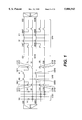
- FIG. 7 shows a chip configuration of the switch-separated type hierarchical data line structure or alternating-positioning-switch type hierarchical data line structure of this invention when a column decoder is shared by a plurality of column switches arranged in the data line direction (YS control system).
- This chip consists largely of a memory mat (MAT0) and peripheral circuits. Though not shown in the figure, two or more memory mats can be installed in the chip.
- the memory mat has a hierarchical structure ranging in order of size from sub memory arrays (SMA0, SMA1, . . . ) to unit memory arrays (UA0, UA1, . . . ).
- UA includes primitive unit memory arrays (PUA) containing data line connection switches and global data line separation switches and sense amplifier blocks (SB) containing a sense amplifier, a precharge circuit and a column switch, the primitive unit memory arrays and the sense amplifier blocks being arranged alternately.
- the word lines (W) are arranged vertically and the data lines horizontally.
- the address terminal (A) usually employs an address multiplex system in which a row address (X address) (XAD) and a column address (Y address) (YAD) are entered in a time division fashion.
- XAD is stored in a row address latch (XLTC) by a row address strobe signal (RASB).
- YAD is stored in a column address latch (YLTC) by a column address strobe signal CASB.
- XC row control circuit
- XAD is decoded by a-row decoder (X decoder) (Xdec) to select a corresponding word line W.
- X decoder X decoder
- Ydec column decoder
- Y-selection line Y-selection line
- the column data selected by YS is read out through column switches onto a common input/output line pair (I/O), from which the read data is put out through a read/write circuit (RWC), an output buffer (D0B) and an input/output pin (DQ) to the outside of the chip.
- the memory cells of a column selected by YAD are written with data from outside the chip through the input buffer (DINB), RWC and I/O.
- FIG. 8(a) shows an array (6) that applies the YS control system to the array (1) of the switch-separated type hierarchical data line structure of this invention shown in FIG. 1 (Embodiment 1).
- the YS control system can also be applied similarly to the arrays of other embodiments.
- Data lines in two pairs in the word line direction and four pairs in the data line direction (D0-D0B, D1-D1B, etc.) are connected through data line connection switches to the global data lines (GD0-GD0B to GD2-GD2B) arranged in parallel to the data lines, in order to form a primitive unit memory array (PUA0).
- PDA0 primitive unit memory array
- the global data line pairs GD0-GD0B and GD1-GD1B are connected to each other through QM0T-QM0B and QM1T-QM1B.
- GD1-GD1B and GD2-GD2B are connected to each other through QM2T-QM2B and QM3T-QM3B.
- Global data line pairs at both ends are connected to the sense amplifier blocks (SB).
- SB comprises a CMOS sense amplifier (SA), a precharge circuit (PB) and a column switch (YG).
- SA CMOS sense amplifier
- PB precharge circuit
- YG column switch
- RWC read/write circuit
- MC, SA, PB and YG Detailed circuits of MC, SA, PB and YG are shown in FIG. 8(b), 8(c), 8(d) and 8(e).
- the CMOS sense amplifier SA comprises a pair of PMOS transistors and a pair of NMOS transistors, in which their sources are commonly connected and their gates and drains are cross-connected.
- the output of Ydec is connected with the column selection line (YS), and column switches having the same YAD are controlled commonly by a single YS0.
- a single unit memory array (UA) is divided into a plurality of primitive unit memory arrays and sense amplifier blocks.
- This arrangement offers the advantage of suppressing the signal delay and power consumption in the global data lines when the memory circuit integration enhances and UA becomes long. Further, because a plurality of column switches arranged in the data line direction are controlled commonly by YS, only one Ydec is needed even when the number of divisions of UA is increased. This prevents an increase in the chip area. The similar effect is produced even when the number of memory cells connected to one data line pair, the number of global data line pairs in the primitive unit memory array and the number of primitive unit arrays in one UA differ from those of this embodiment.
- FIG. 2(b) shows a layout of switches in the memory array (6).
- FIG. 9 shows a cross-sectional structure taken along the line B--B' of FIG. 2(b).
- this embodiment requires only one pair of global data lines for two pairs of data lines. Normally, because miniaturization becomes more difficult for upper layers in the wiring layer fabricating process, the upper layers need to have greater line pitches.
- the wiring pitch of this layer is greater than the wiring pitch of the underlying data line layer, thus satisfying the above requirement. Therefore, forming the global data lines and column selection line in the same wiring layer has the advantage of not increasing the number of wiring layers.
- the column selection line by using a wiring layer that is positioned further up above the global data line.
- the line pitch of the column selection line (YS) wiring layer can be widened, so that the coupling capacitance between the wires is reduced, increasing the transmission speed of signals.
- the memory access i.e., the read and write operations to and from the memory cells as performed by the circuit of FIG. 8 will be explained by referring to FIGS. 10 and 11.
- FIG. 10 is a timing chart showing the read operation of the circuit of FIG. 8.
- the precharge signals PC0, PC1 are at 2 V and the global data line separation switch control lines M0 to M3 and the data line connection switch control lines T0 to T3 are at 2.5 V(Vpp). All data lines are precharged to 1 V(Vdd/2) through global data lines.
- RASB is lowered to 0 V(Vss) to determine the row address, after which PC0, PC1, M0 and T1 to T3 are lowered to 0 V. M1 to M3 and T0 are left at 2.5 V.
- D0-D0B is connected to SA0 through DG0-DG0B
- D1-D1B is connected to SA1 through GD1-GD1B and GD2-GD2B, causing D0-D0B and D1-D1B to become floated.
- Other data lines are separated from global data lines.
- W0 is raised to 2.5 V.
- the MC produces a signal of about 0.1 V onto D0, causing a potential difference between D0 and D0B.
- SA0 by changing the sense amplifier NMOS drive line SN0 to 0 V and the sense amplifier PMOS drive line SP0 to 2 V, this potential difference is amplified by SA0.
- a signal is also produced on D1 and is amplified by SA1. Because GD0 and GD1 are isolated by QM0T, data will not collide.
- CASB is lowered to 0 V to determine the column address and YS0 is raised to 2 V to open column switch YG, thereby connecting GD0-GD0B and I/O0-I/O0B.
- I/O0-I/O0B is precharged to 1 V at the initial state but opening YG0 causes the complementary data on the GD0-GD0B to appear on I/O0-I/O0B.
- RWC0 is provided with a bias circuit to reduce the amplitude of the signal on the I/O0-I/O0B to 0.5 V.
- RWC0 amplifies the complementary data on the I/O line pair and sends it to the output buffer, which in turn outputs the data to the outside of the chip.
- CASB returns to 2 V
- YS0 is returned to 0 V to close column switch YG.
- RASB is returned to 2 V
- WL0 is lowered to 0 V to write data from D0 and D1 into the memory cell again.
- SN0, SP0, SN1, and SP1 are returned to 1 V and PC0, PC1, M0, and T1 to T3 are raised to 2.5 V to precharge D0-D0B and D1-D1B to 1 V again, thus completing the read cycle.
- FIG. 11 shows the write operation for writing data into a memory cell at the intersection between W0 and D0.
- controls similar to those of the above read operation are performed to read stored information from the memory cell.
- SA0 controls similar to those of the above read operation are performed to read stored information from the memory cell.
- CASB is lowered to 0 V to determined the column address. This causes the I/O0-I/O0B to be complementarily driven by RWC according to the write data.
- YS0 is raised to 2 V to open YG0 to write data on the I/O0-I/O0B into D0-D0B through GD0-GD0B.
- YS0 After CASB has returned to 2 V, YS0 is returned to 0 V to close YG0.
- RASB has returned to 2 V, the termination operation similar to that of the read cycle is carried out to complete the write cycle.
- FIG. 12 shows the sense amplifier drive circuit SAD in the switch-separated type hierarchical data line structure of this invention.
- This circuit is included in XC.
- a feature of this sense amplifier drive circuit is that the drive capability of the sense amplifier is varied as the load of the sense according to the open or closed state of the global word line separation switches.
- SAD0 includes NMOS transistors DNL0 and DNS0 for driving SN0 and PMOS transistors DPL0 and DPS0 for driving SP0.
- the current drive capability of DNL0 is set larger than that of DNS0. This may be achieved by making the gate lengths of DNL0 and DNS0 equal and the gate width of DNL0 greater. Namely, the conductance of DNL0 is larger than that of DNS0.
- the current drive capability of DPL0 is set to be larger than that of DPS0.
- SAD1 has a similar configuration.
- data line pair D0-D0B is connected to SA0 through a pair GD0-GD0B, and the pair D1-D1B is connected to SA1 through GD1-GD1B and GD2-GD2B.
- GD0 and GD2 are almost equal in length to a data line, whereas GD1 is two times as long as the data line.
- the length of the global data line connected to SA0 is equal to that of the data line, while the length of the global data line connected to SA1 is three times the length of the data line.
- the parasitic capacitance coupled to the sense amplifier is greater for SA1 than for SA0.
- FIG. 10 shows the timing chart for the read operation.
- SAD0 STS0 is raised to 2 V to turn on DNS0 and DPS0
- SAD1 STL1 is raised to 2 V to turn on DNL1 and DPL1. That is, for SA0 with a small load capacity, SN0 and SP0 are driven by DNS0 and DPS0, which have a small drive power.
- SA1 with a large load capacity, SN1 and SP1 are driven by DNL1 and DPL1, which have a large drive power. This makes the amplification rates of SA0 and SA1 almost equal.
- SA1 has a smaller load than SA0, so that STS1 and STL0 are raised to 2 V to drive SN0 and SP0 by DNL0 and DPL0 that have a large drive power.
- the sense amplifier driver circuits SAD can be modified to the following.
- the variation of current is attained by the combination of the control signals STS and STL: turning ON only STS for small current mode and turning ON both STS and STL for large current mode.
- You might use the multi-step voltage control for STS such as 0V, 0.5V, 1V, 1.5V, and 2V. This might allow to delete DNL and DPL, if you choose appropriate transistor size for DNS and DPS.
- This scheme is also useful for precise control of the current for sense amplifier depending on the length of global data line. If you want full digital control for STS, you can use MOS transistors coupled in parallel for the same purpose.
- this system has the advantage that even if there is an imbalance in the length between global data lines, there is no possibility of SA0, whose load is small, being amplified too fast, thereby keeping the S/N ratio from deteriorating.
- a drive system of FIG. 13 may be used to eliminate influences of the load imbalance due to cell capacitance between paired input lines of the sense amplifiers. After W0 is raised to 2.5 V to read signals onto D0 and GD0, T0 is lowered to 0 V instantaneously to raise the resistance of QT and start the sense amplifiers. Because the amplification is carried out with SA0 isolated from D0 and D0B with high resistance and the cell capacitance can hardly be seen from the sense amplifiers, the loads of the paired input lines becomes equal, increasing the S/N ratio.
- FIG. 14 shows a memory array (7) of this invention, that uses a variation of PUAO of FIG. 8 with some parts not shown.
- This embodiment is a variation of the array (4) of FIG. 5.
- this embodiment has an NMOS sense amplifier NSA, rather than a CMOS sense amplifier SA, on the data lines and a PMOS sense amplifier PSA in the sense amplifier block on the global data lines in the array (4) of FIG. 5.
- Other data line pairs have the similar configuration to that of D0-D0B and D1-D1B.
- the arranging of the NMOS sense amplifier NSA on data lines eliminates the need to provide an N/P isolation region for each data line.
- the N/P isolation region is required on only the PMOS sense amplifier PSA portion on global data lines.
- arranging the NMOS sense amplifier NSA on data lines causes little increase in the chip area.
- PMOS is used as the transfer gate of a memory cell
- a PMOS sense amplifier PSA instead of the CMOS sense amplifier SA is provided on the data lines, and an NMOS sense amplifier NSA in the sense amplifier block on the global data lines in the array (4) of FIG. 5.
- T0 to T7 are all closed and W0 is activated to read signals onto D0 and D1.
- SN0 and SN1 are lowered to 0 V to amplify the signals.
- the paired data lines are amplified almost to 0 V and 1 V.
- T0 and T1 are opened to read signals onto GD0 and GD1, after which SP0 and SP1 are raised to 2 V to amplify the data lines to 0 V and 2 V, respectively.
- This embodiment therefore is effective to enhance S/N when the chip capacity is increased and the primitive unit memory array (PUA) becomes long.
- this array has the data line connection switches (QT) arranged in alternate positions, it is possible to set length of the NMOS sense amplifiers (NSAs) in the word line direction equal to two pairs of data lines.
- FIG. 15 shows a memory array (8) of this invention.
- This figure shows a variation of PUAO of FIG. 8 with some parts not shown.
- This embodiment is a variation of the array (4) of FIG. 5.
- this embodiment provides an NMOS sense amplifier DSA on the data lines and a CMOS sense amplifier SA in the sense amplifier block on the global data lines.
- NMOS sense amplifier DSA is a voltage-to-current converter circuit (or voltage-to-current conversion type sense amplifier circuit).
- Other data line pairs have the similar configuration to that of D0-D0B and D1-D1B.
- NMOS sense amplifier DSA uses NMOS transistors
- arranging NMOS sense amplifier DSA on the data lines eliminates the need for providing an N/P isolation region for each data line.
- the NIP isolation region is required only for the sense amplifier portion on the global data lines; Hence, providing the NMOS sense amplifier DSA on the data lines will result in only a slight increase in the chip area.
- PMOS is used for the transfer gate of a memory cell
- a PMOS sense amplifier DSA is provided on the data lines.
- all write related data line connection switch control lines are at 2.5 V
- all read related data line connection switch control lines are at 0 V
- M0 and M1 are at 2.5 V.
- TW write related data line connection switch control lines
- TR read related data line connection switch control lines
- M0 and M1 are at 2.5 V.
- W0 is raised to 2.5 V to read a signal onto D0 and the voltage difference between D0 and D0B is converted into a current difference by DSA0.
- the current difference between GD0 and GD0B is transmitted to RWC0 through YG and I0 in SB0 by raising YS to 2 V.
- SP0 of SA0 is driven to 2 V and SN0 to 0 V to amplify GD0 and GD0B to 0 V and 2 V, respectively.
- the signal on D1 is similarly processed by SB1.
- TR0 and TR1 are lowered to 0 V and TW0 and TW1 are raised to 2.5 V to write a voltage of 0 V or 2 V into the memory cells.
- this embodiment is effective to enhance S/N when, for example, chip capacity is increased and the primitive unit memory array PUA becomes long. Because information is not read out undesirably even when TR and YS are raised before W is raised to 2.5 V, the timing margin at this portion is eliminated, assuring a faster reading operation.
- this array has the data line connection switches (QT) arranged at alternate positions, it is possible to make the length of each NMOS sense amplifier DSA in the word line direction as long as two data line pairs, facilitating the design of layout.
- FIG. 19 shows twisted (or transposed) global data lines (1) of this invention. This is an example in which global data lines are twisted to reduce the coupling noise between global data lines.
- the sense amplifier block SB includes a CMOS sense amplifier, a precharge circuit and a column switch, all shown in FIG. 8. This diagram does not show data lines and data line connection switches.
- the memory array has the following configuration. Two global data lines and two global data line separation switches together-form a group of global data lines GDG. Two such groups (GDGs) form a global data line unit GDU.
- the memory array has the GDU repetitively arranged in the data line direction and in the word line direction.
- At least two sense amplifier blocks SB are connected to each column of global data lines in which GDGs are arranged in the data line direction.
- GDG1 global data lines are twisted in the region of QM2 and, in GDG2, are twisted in the region of QM6.
- GDG2 global data lines are twisted in the region of SWB1 in FIG. 1.
- SWB4 In the alternating-positioning-switch type, they are twisted in the region of SWB4 of FIG. 5.
- first main data line pair there is a first main data line pair, which is then divided into a plurality of parts of equal lengths (five sections of GD0, GD1, GD2, GD3 and GD4).
- the dividing points are connected by main data line separation switches (QL0, QM0, QM1, QM2, QM3, QMR0).
- main data line separation switches QL0, QM0, QM1, QM2, QM3, QMR0.
- main data line separation switches are assigned from left to right with numbers beginning with 1 (note that the numbers do not correspond to the reference numerals), and the paired main data lines are twisted near or inside the even-numbered main data line separation switches (QM0, QM2, QMR0).
- the paired main data lines are twisted near or inside the odd-numbered main data line separation switches (QML1, QM6, QM8).
- QML1, QM6, QM8 odd-numbered main data line separation switches
- GD0 for example, is not separated at SB0 but is extended to the array on the opposite side, that global data lines on both sides share SB and are separated by QM in the array on the opposite side.
- all global data lines are almost equal in length and cross almost the same number of word lines.
- the connection position of SB is set at nearly the middle of the global data lines.
- GD9 receives a negative coupling from GD4B
- GD6 receives a positive coupling from GD1.
- GD9 and GD6 are both 256 W long and thus their positive and negative couplings are canceled out.
- I3B GD8B receives a negative coupling from GD3B
- GD7B receives a positive coupling from GD2.
- GD8B and GD7B are both 256 W long and thus their positive and negative couplings are canceled out. Because the noise I3 and I3B receive are canceled out, the operation margin of SA in SB3 does not deteriorate.
- the twisted global data lines of this invention has the advantage of no coupling imbalance in the worst case and of being able to cancel noise completely.
- FIG. 21 shows a switch layout of the alternating-positioning-switch type when the global data lines are twisted at SWB4 in FIG. 5. This can be laid out in the length of 9 F in the data line direction, realizing the data line twisting with small overhead compared with 7 F of FIG. 18.
- FIG. 20 shows twisted global data lines (2) of this invention.
- GD has a length of 1024 word lines and D has a length of 128 word lines.
- the sense amplifier block SB includes a CMOS sense amplifier, a precharge circuit and a column switch, all shown in FIG. 8. Data lines and data line connection switches are not shown.
- the memory array is constructed as follows. Two global data lines (GDs) and two global data line separation switches (QMs) form a global data line group GDG. Two GDGs form a global data line unit GDU.
- the memory array has the GDU repetitively arranged in the data line direction and in the word line direction.
- At least two sense amplifier blocks SB are connected to each column of global data lines in which GDGs are arranged in the data line direction.
- GDG1 has its global data lines twisted at the middle of GD2
- GDG2 has its global data lines twisted at the middle of GD6.
- the twisting position is located in a region of SB and, in the switch-separated type, at the mid-point of GD1 of FIG. 1 and, in the alternating-positioning-switch type, at SWB5 of FIG. 5.
- the main data lines are divided into sections of equal lengths as in the previous embodiment. While in FIG. 19 the twisting position is set near the global data line separation switches at the main data line dividing positions, this embodiment has the twisting position at the mid-point between the dividing positions.
- GD0 is not separated at SB0 but extended to the array on the opposite side.
- Global data lines on both sides share SB and are separated by global data line connection switches in the array on the opposite side.
- all global data lines are almost equal in length and cross roughly the same number of word lines.
- the connection position of SB is set at almost the middle of the global data line.
- the twisting is done at the central part of global data lines so that the neighboring global data lines, such as GD1-GD1B and GD6-GD6B, can cancel their noise.
- This offers the advantage that not only in the worst case but also when data is read out from any data lines there is no coupling imbalance so that noise can be canceled out completely.
- the twisted global data lines of this invention therefore, offer an advantage in that no coupling imbalance occurs, whichever data lines signals are read from, thus assuring complete canceling of noise.
- FIG. 22 shows a layout of switches of the alternating-positioning-switch type when global data lines are twisted at SWB5 portion in FIG. 5. This can be formed in the length of 7 F in the data line direction and the data line twisting can be realized with small overhead compared with 5 F of FIG. 18(b).
- this configuration can divide data lines into multiple sections virtually without increasing the chip area and can also reduce power consumption.
Abstract
Description
Vn(0)=A·Cs· K0/(Cd+Cgd)! (1/2) (1)
Vn(1)=A·Cs· K1/(Cd+3Cgd)! (1/2) (2)
Claims (39)
Applications Claiming Priority (2)
| Application Number | Priority Date | Filing Date | Title |
|---|---|---|---|
| JP24593196 | 1996-09-18 | ||
| JP8-245931 | 1996-09-18 |
Publications (1)
| Publication Number | Publication Date |
|---|---|
| US5886943A true US5886943A (en) | 1999-03-23 |
Family
ID=17140993
Family Applications (1)
| Application Number | Title | Priority Date | Filing Date |
|---|---|---|---|
| US08/931,528 Expired - Lifetime US5886943A (en) | 1996-09-18 | 1997-09-16 | Semiconductor memory having a hierarchical data line structure |
Country Status (1)
| Country | Link |
|---|---|
| US (1) | US5886943A (en) |
Cited By (25)
| Publication number | Priority date | Publication date | Assignee | Title |
|---|---|---|---|---|
| US6269029B1 (en) | 1999-06-29 | 2001-07-31 | Hyundai Electronics Industries, Co., Ltd. | Semi-conductor memory device |
| US6335899B1 (en) * | 2000-04-19 | 2002-01-01 | Lsi Logic Corporation | Compensation capacitance for minimizing bit line coupling in multiport memory |
| US6370054B1 (en) * | 1999-11-04 | 2002-04-09 | Hitachi, Ltd. | Dynamic RAM and semiconductor device |
| US6418063B1 (en) * | 1997-12-17 | 2002-07-09 | Silicon Aquarius, Inc. | Memory architecture and systems and methods using the same |
| US20020141633A1 (en) * | 2001-03-29 | 2002-10-03 | Kazuhiro Nakashima | Pattern data converting method and apparatus |
| US20030063505A1 (en) * | 2001-09-28 | 2003-04-03 | Richard Ferrant | Dram |
| US6545933B2 (en) * | 2000-03-29 | 2003-04-08 | Hitachi, Ltd. | Semiconductor memory |
| US20030067833A1 (en) * | 2001-10-08 | 2003-04-10 | Jong Hoon Hong | Bit line selection circuit having hierarchical structure |
| US20030116827A1 (en) * | 2001-12-20 | 2003-06-26 | Yvon Savaria | Methods, apparatus, and systems for reducing interference on nearby conductors |
| US20030117183A1 (en) * | 2001-12-20 | 2003-06-26 | Claude Thibeault | Methods, apparatus, and systems for reducing interference on nearby conductors |
| US20030117184A1 (en) * | 2001-12-20 | 2003-06-26 | Karl Fecteau | Methods, apparatus, and systems for reducing interference on nearby conductors |
| US6657913B2 (en) * | 2000-07-28 | 2003-12-02 | Micron Technology, Inc. | Array organization for high-performance memory devices |
| US20040017691A1 (en) * | 2002-07-29 | 2004-01-29 | Luk Wing K. | Multiple subarray DRAM having a single shared sense amplifier |
| US6703868B2 (en) | 2001-12-20 | 2004-03-09 | Hyperchip Inc. | Methods, apparatus, and systems for reducing interference on nearby conductors |
| US20040136251A1 (en) * | 2000-02-04 | 2004-07-15 | Renesas Technology Corporation | Semiconductor device |
| DE10014112B4 (en) * | 1999-09-03 | 2004-07-22 | Samsung Electronics Co., Ltd., Suwon | Multi-bank memory device and method for arranging input / output lines |
| US20050024916A1 (en) * | 2003-07-30 | 2005-02-03 | Hynix Semiconductor Inc. | Cell array block of feram, and feram using cell array |
| US6874136B2 (en) * | 2002-01-10 | 2005-03-29 | M2000 | Crossbar device with reduced parasitic capacitive loading and usage of crossbar devices in reconfigurable circuits |
| US20060092682A1 (en) * | 2004-10-29 | 2006-05-04 | Samsung Electronics Co., Ltd. | Semiconductor memory device and a method for arranging signal lines thereof |
| EP1659591A2 (en) | 2002-08-29 | 2006-05-24 | Fujitsu Limited | Semiconductor memory |
| US20060180939A1 (en) * | 2005-02-16 | 2006-08-17 | Matsushita Electric Industrial Co., Ltd. | Tamper-resistant semiconductor device |
| US20080165559A1 (en) * | 2007-01-04 | 2008-07-10 | Samsung Electronics Co., Ltd. | Data line layout and line driving method in semiconductor memory device |
| EP2159799A1 (en) * | 2008-08-27 | 2010-03-03 | Panasonic Corporation | Semiconductor memory with shared global busses for reconfigurable logic device |
| US20120170356A1 (en) * | 2009-09-01 | 2012-07-05 | Rambus Inc. | Semiconductor Memory Device with Hierarchical Bitlines |
| KR20140048413A (en) * | 2012-10-12 | 2014-04-24 | 에스케이하이닉스 주식회사 | Semiconductor memory device |
Citations (6)
| Publication number | Priority date | Publication date | Assignee | Title |
|---|---|---|---|---|
| JPH0612862A (en) * | 1992-03-18 | 1994-01-21 | Gold Star Electron Co Ltd | One-intersection-point type dram having bidirectional common bit line |
| JPH07211059A (en) * | 1993-11-30 | 1995-08-11 | Mitsubishi Electric Corp | Semiconductor memory device |
| US5495440A (en) * | 1993-01-19 | 1996-02-27 | Mitsubishi Denki Kabushiki Kaisha | Semiconductor memory device having hierarchical bit line structure |
| US5561626A (en) * | 1994-11-28 | 1996-10-01 | Fujitsu Limited | Semiconductor memory with hierarchical bit lines |
| US5600602A (en) * | 1995-04-05 | 1997-02-04 | Micron Technology, Inc. | Hierarchical memory array structure having electrically isolated bit lines for temporary data storage |
| US5682343A (en) * | 1993-08-20 | 1997-10-28 | Mitsubishi Denki Kabushiki Kaisha | Hierarchical bit line arrangement in a semiconductor memory |
-
1997
- 1997-09-16 US US08/931,528 patent/US5886943A/en not_active Expired - Lifetime
Patent Citations (8)
| Publication number | Priority date | Publication date | Assignee | Title |
|---|---|---|---|---|
| JPH0612862A (en) * | 1992-03-18 | 1994-01-21 | Gold Star Electron Co Ltd | One-intersection-point type dram having bidirectional common bit line |
| US5367488A (en) * | 1992-03-18 | 1994-11-22 | Goldstar Electron Co., Ltd. | DRAM having bidirectional global bit lines |
| US5495440A (en) * | 1993-01-19 | 1996-02-27 | Mitsubishi Denki Kabushiki Kaisha | Semiconductor memory device having hierarchical bit line structure |
| US5682343A (en) * | 1993-08-20 | 1997-10-28 | Mitsubishi Denki Kabushiki Kaisha | Hierarchical bit line arrangement in a semiconductor memory |
| JPH07211059A (en) * | 1993-11-30 | 1995-08-11 | Mitsubishi Electric Corp | Semiconductor memory device |
| US5610871A (en) * | 1993-11-30 | 1997-03-11 | Mitsubishi Denki Kabushiki Kaisha | Semiconductor memory device having a hierarchical bit line structure with reduced interference noise |
| US5561626A (en) * | 1994-11-28 | 1996-10-01 | Fujitsu Limited | Semiconductor memory with hierarchical bit lines |
| US5600602A (en) * | 1995-04-05 | 1997-02-04 | Micron Technology, Inc. | Hierarchical memory array structure having electrically isolated bit lines for temporary data storage |
Non-Patent Citations (4)
| Title |
|---|
| J.H. Ahn et al, "Bidirectional Matched Global Bit Line Scheme for High Density DRAMs", 1993 Symposium on VLSI Circuits Digest of Technical Papers, 1993, pp. 91-92. |
| J.H. Ahn et al, Bidirectional Matched Global Bit Line Scheme for High Density DRAMs , 1993 Symposium on VLSI Circuits Digest of Technical Papers, 1993, pp. 91 92. * |
| Kyoo Itoh, "Ultra-LSI Memory", published by Baifukan, 1994, pp. 191-237. |
| Kyoo Itoh, Ultra LSI Memory , published by Baifukan, 1994, pp. 191 237. * |
Cited By (58)
| Publication number | Priority date | Publication date | Assignee | Title |
|---|---|---|---|---|
| US6418063B1 (en) * | 1997-12-17 | 2002-07-09 | Silicon Aquarius, Inc. | Memory architecture and systems and methods using the same |
| US6269029B1 (en) | 1999-06-29 | 2001-07-31 | Hyundai Electronics Industries, Co., Ltd. | Semi-conductor memory device |
| DE10014112B4 (en) * | 1999-09-03 | 2004-07-22 | Samsung Electronics Co., Ltd., Suwon | Multi-bank memory device and method for arranging input / output lines |
| US7474550B2 (en) | 1999-11-04 | 2009-01-06 | Elpida Memory, Inc. | Dynamic RAM-and semiconductor device |
| US20040233770A1 (en) * | 1999-11-04 | 2004-11-25 | Hiroki Fujisawa | Dynamic ram-and semiconductor device |
| US6370054B1 (en) * | 1999-11-04 | 2002-04-09 | Hitachi, Ltd. | Dynamic RAM and semiconductor device |
| US6373776B2 (en) * | 1999-11-04 | 2002-04-16 | Hitachi, Ltd. | Dynamic ram and semiconductor device |
| US6762949B2 (en) | 1999-11-04 | 2004-07-13 | Hitachi, Ltd. | Dynamic RAM-and semiconductor device |
| US7221576B2 (en) | 1999-11-04 | 2007-05-22 | Elpida Memory, Inc. | Dynamic RAM-and semiconductor device |
| US6545897B2 (en) | 1999-11-04 | 2003-04-08 | Hitachi, Ltd. | Dynamic RAM-and semiconductor device |
| US20040017716A1 (en) * | 1999-11-04 | 2004-01-29 | Hiroki Fujisawa | Dynamic RAM-and semiconductor device |
| US6639822B2 (en) | 1999-11-04 | 2003-10-28 | Hitachi, Ltd. | Dynamic ram-and semiconductor device |
| US8199549B2 (en) | 2000-02-04 | 2012-06-12 | Renesas Electronics Corporation | Semiconductor device |
| US7813156B2 (en) * | 2000-02-04 | 2010-10-12 | Renesas Technology Corp. | Semiconductor device |
| US20090027984A1 (en) * | 2000-02-04 | 2009-01-29 | Renesas Technology Corp. | Semiconductor device |
| US20060146623A1 (en) * | 2000-02-04 | 2006-07-06 | Renesas Technology Corp. | Semiconductor device |
| US20070291564A1 (en) * | 2000-02-04 | 2007-12-20 | Hiroyuki Mizuno | Semiconductor device |
| US7126868B2 (en) | 2000-02-04 | 2006-10-24 | Renesas Technology Corp. | Semiconductor device |
| US7242627B2 (en) | 2000-02-04 | 2007-07-10 | Renesas Technology Corp. | Semiconductor device |
| US7436722B2 (en) | 2000-02-04 | 2008-10-14 | Renesas Technology Corp. | Semiconductor device |
| US6990002B2 (en) * | 2000-02-04 | 2006-01-24 | Renesas Technology Corp. | Semiconductor device |
| US20040136251A1 (en) * | 2000-02-04 | 2004-07-15 | Renesas Technology Corporation | Semiconductor device |
| US8605478B2 (en) | 2000-02-04 | 2013-12-10 | Renesas Electronics Corporation | Semiconductor device |
| US6545933B2 (en) * | 2000-03-29 | 2003-04-08 | Hitachi, Ltd. | Semiconductor memory |
| KR100887333B1 (en) * | 2000-03-29 | 2009-03-06 | 엘피다 메모리, 아이엔씨. | Semiconductor memory |
| US6335899B1 (en) * | 2000-04-19 | 2002-01-01 | Lsi Logic Corporation | Compensation capacitance for minimizing bit line coupling in multiport memory |
| US6657913B2 (en) * | 2000-07-28 | 2003-12-02 | Micron Technology, Inc. | Array organization for high-performance memory devices |
| US20020141633A1 (en) * | 2001-03-29 | 2002-10-03 | Kazuhiro Nakashima | Pattern data converting method and apparatus |
| US7020321B2 (en) * | 2001-03-29 | 2006-03-28 | Kabushiki Kaisha Toshiba | Pattern data converting method and apparatus |
| FR2830365A1 (en) * | 2001-09-28 | 2003-04-04 | St Microelectronics Sa | DYNAMIC VIVE MEMORY |
| US20030063505A1 (en) * | 2001-09-28 | 2003-04-03 | Richard Ferrant | Dram |
| US6798681B2 (en) | 2001-09-28 | 2004-09-28 | Stmicroelectronics S.A. | Dram |
| US20030067833A1 (en) * | 2001-10-08 | 2003-04-10 | Jong Hoon Hong | Bit line selection circuit having hierarchical structure |
| US6728125B2 (en) * | 2001-10-08 | 2004-04-27 | Hynix Semiconductor Inc. | Bit line selection circuit having hierarchical structure |
| US6897497B2 (en) | 2001-12-20 | 2005-05-24 | Hyperchip Inc. | Methods, apparatus, and systems for reducing interference on nearby conductors |
| US20030117184A1 (en) * | 2001-12-20 | 2003-06-26 | Karl Fecteau | Methods, apparatus, and systems for reducing interference on nearby conductors |
| US7609778B2 (en) | 2001-12-20 | 2009-10-27 | Richard S. Norman | Methods, apparatus, and systems for reducing interference on nearby conductors |
| US20030116827A1 (en) * | 2001-12-20 | 2003-06-26 | Yvon Savaria | Methods, apparatus, and systems for reducing interference on nearby conductors |
| US6703868B2 (en) | 2001-12-20 | 2004-03-09 | Hyperchip Inc. | Methods, apparatus, and systems for reducing interference on nearby conductors |
| US20030117183A1 (en) * | 2001-12-20 | 2003-06-26 | Claude Thibeault | Methods, apparatus, and systems for reducing interference on nearby conductors |
| US6874136B2 (en) * | 2002-01-10 | 2005-03-29 | M2000 | Crossbar device with reduced parasitic capacitive loading and usage of crossbar devices in reconfigurable circuits |
| US20040017691A1 (en) * | 2002-07-29 | 2004-01-29 | Luk Wing K. | Multiple subarray DRAM having a single shared sense amplifier |
| US6768692B2 (en) * | 2002-07-29 | 2004-07-27 | International Business Machines Corporation | Multiple subarray DRAM having a single shared sense amplifier |
| EP1659591A3 (en) * | 2002-08-29 | 2006-06-07 | Fujitsu Limited | Semiconductor memory |
| EP1659591A2 (en) | 2002-08-29 | 2006-05-24 | Fujitsu Limited | Semiconductor memory |
| US6867998B2 (en) * | 2003-07-30 | 2005-03-15 | Hynix Semiconductor Inc. | Cell array block of FeRAM, and FeRAM using cell array |
| US20050024916A1 (en) * | 2003-07-30 | 2005-02-03 | Hynix Semiconductor Inc. | Cell array block of feram, and feram using cell array |
| US20060092682A1 (en) * | 2004-10-29 | 2006-05-04 | Samsung Electronics Co., Ltd. | Semiconductor memory device and a method for arranging signal lines thereof |
| US7280383B2 (en) * | 2004-10-29 | 2007-10-09 | Samsung Electronics Co., Ltd. | Semiconductor memory device and a method for arranging signal lines thereof |
| US20060180939A1 (en) * | 2005-02-16 | 2006-08-17 | Matsushita Electric Industrial Co., Ltd. | Tamper-resistant semiconductor device |
| US7547973B2 (en) * | 2005-02-16 | 2009-06-16 | Panasonic Corporation | Tamper-resistant semiconductor device |
| US20080165559A1 (en) * | 2007-01-04 | 2008-07-10 | Samsung Electronics Co., Ltd. | Data line layout and line driving method in semiconductor memory device |
| US7697314B2 (en) * | 2007-01-04 | 2010-04-13 | Samsung Electronics Co., Ltd. | Data line layout and line driving method in semiconductor memory device |
| US20100054072A1 (en) * | 2008-08-27 | 2010-03-04 | Anthony Stansfield | Distributed block ram |
| EP2159799A1 (en) * | 2008-08-27 | 2010-03-03 | Panasonic Corporation | Semiconductor memory with shared global busses for reconfigurable logic device |
| US20120170356A1 (en) * | 2009-09-01 | 2012-07-05 | Rambus Inc. | Semiconductor Memory Device with Hierarchical Bitlines |
| US8717797B2 (en) * | 2009-09-01 | 2014-05-06 | Rambus Inc. | Semiconductor memory device with hierarchical bitlines |
| KR20140048413A (en) * | 2012-10-12 | 2014-04-24 | 에스케이하이닉스 주식회사 | Semiconductor memory device |
Similar Documents
| Publication | Publication Date | Title |
|---|---|---|
| US5886943A (en) | Semiconductor memory having a hierarchical data line structure | |
| US5973983A (en) | Semiconductor memory device having a hierarchical bit line structure with reduced interference noise | |
| US4748591A (en) | Semiconductor memory | |
| US5495440A (en) | Semiconductor memory device having hierarchical bit line structure | |
| US7616512B2 (en) | Semiconductor memory device with hierarchical bit line structure | |
| US5682343A (en) | Hierarchical bit line arrangement in a semiconductor memory | |
| US8493807B2 (en) | Semiconductor device having hierarchically structured bit lines and system including the same | |
| US5282175A (en) | Semiconductor memory device of divided word line | |
| JPH04159689A (en) | Semiconductor memory | |
| JPH0424799B2 (en) | ||
| US5016224A (en) | Semiconductor memory device | |
| EP0813208B1 (en) | Semiconductor memory device | |
| US20080037309A1 (en) | Semiconductor memory device | |
| US6275407B1 (en) | Semiconductor memory device having sense and data lines for use to read and write operations | |
| KR20000071473A (en) | Semiconductor memory device | |
| US4803664A (en) | Dynamic random access memory having a gain function | |
| KR960016426B1 (en) | Semiconductor integrated circuit device | |
| JP3936005B2 (en) | Semiconductor memory device | |
| US5818773A (en) | Semiconductor storage device | |
| US6097654A (en) | Semiconductor memory | |
| JP3557051B2 (en) | Semiconductor storage device | |
| JP4264633B2 (en) | Semiconductor memory device | |
| JPS6054471A (en) | Semiconductor memory | |
| EP0169460B1 (en) | Dynamic memory array with segmented and quasi-folded bit lines | |
| JP3553850B2 (en) | Semiconductor memory device |
Legal Events
| Date | Code | Title | Description |
|---|---|---|---|
| AS | Assignment |
Owner name: HITACHI, LTD., JAPAN Free format text: ASSIGNMENT OF ASSIGNORS INTEREST;ASSIGNORS:SEKIGUCHI, TOMONORI;ITOH, KIYOO;REEL/FRAME:009665/0413 Effective date: 19970902 |
|
| STCF | Information on status: patent grant |
Free format text: PATENTED CASE |
|
| FEPP | Fee payment procedure |
Free format text: PAYOR NUMBER ASSIGNED (ORIGINAL EVENT CODE: ASPN); ENTITY STATUS OF PATENT OWNER: LARGE ENTITY |
|
| FPAY | Fee payment |
Year of fee payment: 4 |
|
| FEPP | Fee payment procedure |
Free format text: PAYOR NUMBER ASSIGNED (ORIGINAL EVENT CODE: ASPN); ENTITY STATUS OF PATENT OWNER: LARGE ENTITY Free format text: PAYER NUMBER DE-ASSIGNED (ORIGINAL EVENT CODE: RMPN); ENTITY STATUS OF PATENT OWNER: LARGE ENTITY |
|
| FPAY | Fee payment |
Year of fee payment: 8 |
|
| FPAY | Fee payment |
Year of fee payment: 12 |
|
| AS | Assignment |
Owner name: RENESAS ELECTRONICS CORPORATION, JAPAN Free format text: ASSIGNMENT OF ASSIGNORS INTEREST;ASSIGNOR:HITACHI, LTD.;REEL/FRAME:026109/0528 Effective date: 20110307 |