US5889652A - C4-GT stand off rigid flex interposer - Google Patents
C4-GT stand off rigid flex interposer Download PDFInfo
- Publication number
- US5889652A US5889652A US08/837,596 US83759697A US5889652A US 5889652 A US5889652 A US 5889652A US 83759697 A US83759697 A US 83759697A US 5889652 A US5889652 A US 5889652A
- Authority
- US
- United States
- Prior art keywords
- integrated circuit
- substrate
- package
- circuit board
- recited
- Prior art date
- Legal status (The legal status is an assumption and is not a legal conclusion. Google has not performed a legal analysis and makes no representation as to the accuracy of the status listed.)
- Expired - Fee Related
Links
- 239000000758 substrate Substances 0.000 claims abstract description 40
- 229910000679 solder Inorganic materials 0.000 claims abstract description 19
- 125000006850 spacer group Chemical group 0.000 claims abstract description 10
- 239000004519 grease Substances 0.000 claims abstract description 9
- 229920001971 elastomer Polymers 0.000 claims description 6
- 239000000806 elastomer Substances 0.000 claims description 6
- 239000004593 Epoxy Substances 0.000 description 6
- 238000000034 method Methods 0.000 description 4
- 239000004642 Polyimide Substances 0.000 description 3
- 239000000463 material Substances 0.000 description 3
- 229920001721 polyimide Polymers 0.000 description 3
- 239000002131 composite material Substances 0.000 description 1
- 239000004020 conductor Substances 0.000 description 1
- 230000006698 induction Effects 0.000 description 1
- 239000004033 plastic Substances 0.000 description 1
- 229920003223 poly(pyromellitimide-1,4-diphenyl ether) Polymers 0.000 description 1
- 230000035939 shock Effects 0.000 description 1
Images
Classifications
-
- H—ELECTRICITY
- H01—ELECTRIC ELEMENTS
- H01L—SEMICONDUCTOR DEVICES NOT COVERED BY CLASS H10
- H01L23/00—Details of semiconductor or other solid state devices
- H01L23/48—Arrangements for conducting electric current to or from the solid state body in operation, e.g. leads, terminal arrangements ; Selection of materials therefor
- H01L23/488—Arrangements for conducting electric current to or from the solid state body in operation, e.g. leads, terminal arrangements ; Selection of materials therefor consisting of soldered or bonded constructions
- H01L23/498—Leads, i.e. metallisations or lead-frames on insulating substrates, e.g. chip carriers
- H01L23/49827—Via connections through the substrates, e.g. pins going through the substrate, coaxial cables
-
- H—ELECTRICITY
- H01—ELECTRIC ELEMENTS
- H01L—SEMICONDUCTOR DEVICES NOT COVERED BY CLASS H10
- H01L23/00—Details of semiconductor or other solid state devices
- H01L23/34—Arrangements for cooling, heating, ventilating or temperature compensation ; Temperature sensing arrangements
- H01L23/42—Fillings or auxiliary members in containers or encapsulations selected or arranged to facilitate heating or cooling
- H01L23/433—Auxiliary members in containers characterised by their shape, e.g. pistons
-
- H—ELECTRICITY
- H01—ELECTRIC ELEMENTS
- H01L—SEMICONDUCTOR DEVICES NOT COVERED BY CLASS H10
- H01L23/00—Details of semiconductor or other solid state devices
- H01L23/48—Arrangements for conducting electric current to or from the solid state body in operation, e.g. leads, terminal arrangements ; Selection of materials therefor
- H01L23/488—Arrangements for conducting electric current to or from the solid state body in operation, e.g. leads, terminal arrangements ; Selection of materials therefor consisting of soldered or bonded constructions
- H01L23/498—Leads, i.e. metallisations or lead-frames on insulating substrates, e.g. chip carriers
- H01L23/4985—Flexible insulating substrates
-
- H—ELECTRICITY
- H01—ELECTRIC ELEMENTS
- H01L—SEMICONDUCTOR DEVICES NOT COVERED BY CLASS H10
- H01L2224/00—Indexing scheme for arrangements for connecting or disconnecting semiconductor or solid-state bodies and methods related thereto as covered by H01L24/00
- H01L2224/01—Means for bonding being attached to, or being formed on, the surface to be connected, e.g. chip-to-package, die-attach, "first-level" interconnects; Manufacturing methods related thereto
- H01L2224/10—Bump connectors; Manufacturing methods related thereto
- H01L2224/15—Structure, shape, material or disposition of the bump connectors after the connecting process
- H01L2224/16—Structure, shape, material or disposition of the bump connectors after the connecting process of an individual bump connector
- H01L2224/161—Disposition
- H01L2224/16151—Disposition the bump connector connecting between a semiconductor or solid-state body and an item not being a semiconductor or solid-state body, e.g. chip-to-substrate, chip-to-passive
- H01L2224/16221—Disposition the bump connector connecting between a semiconductor or solid-state body and an item not being a semiconductor or solid-state body, e.g. chip-to-substrate, chip-to-passive the body and the item being stacked
- H01L2224/16225—Disposition the bump connector connecting between a semiconductor or solid-state body and an item not being a semiconductor or solid-state body, e.g. chip-to-substrate, chip-to-passive the body and the item being stacked the item being non-metallic, e.g. insulating substrate with or without metallisation
-
- H—ELECTRICITY
- H01—ELECTRIC ELEMENTS
- H01L—SEMICONDUCTOR DEVICES NOT COVERED BY CLASS H10
- H01L2224/00—Indexing scheme for arrangements for connecting or disconnecting semiconductor or solid-state bodies and methods related thereto as covered by H01L24/00
- H01L2224/73—Means for bonding being of different types provided for in two or more of groups H01L2224/10, H01L2224/18, H01L2224/26, H01L2224/34, H01L2224/42, H01L2224/50, H01L2224/63, H01L2224/71
- H01L2224/732—Location after the connecting process
- H01L2224/73251—Location after the connecting process on different surfaces
- H01L2224/73253—Bump and layer connectors
-
- H—ELECTRICITY
- H01—ELECTRIC ELEMENTS
- H01L—SEMICONDUCTOR DEVICES NOT COVERED BY CLASS H10
- H01L2924/00—Indexing scheme for arrangements or methods for connecting or disconnecting semiconductor or solid-state bodies as covered by H01L24/00
- H01L2924/30—Technical effects
- H01L2924/301—Electrical effects
- H01L2924/3011—Impedance
-
- Y—GENERAL TAGGING OF NEW TECHNOLOGICAL DEVELOPMENTS; GENERAL TAGGING OF CROSS-SECTIONAL TECHNOLOGIES SPANNING OVER SEVERAL SECTIONS OF THE IPC; TECHNICAL SUBJECTS COVERED BY FORMER USPC CROSS-REFERENCE ART COLLECTIONS [XRACs] AND DIGESTS
- Y10—TECHNICAL SUBJECTS COVERED BY FORMER USPC
- Y10T—TECHNICAL SUBJECTS COVERED BY FORMER US CLASSIFICATION
- Y10T29/00—Metal working
- Y10T29/49—Method of mechanical manufacture
- Y10T29/49002—Electrical device making
- Y10T29/49117—Conductor or circuit manufacturing
- Y10T29/49124—On flat or curved insulated base, e.g., printed circuit, etc.
- Y10T29/4913—Assembling to base an electrical component, e.g., capacitor, etc.
- Y10T29/49144—Assembling to base an electrical component, e.g., capacitor, etc. by metal fusion
-
- Y—GENERAL TAGGING OF NEW TECHNOLOGICAL DEVELOPMENTS; GENERAL TAGGING OF CROSS-SECTIONAL TECHNOLOGIES SPANNING OVER SEVERAL SECTIONS OF THE IPC; TECHNICAL SUBJECTS COVERED BY FORMER USPC CROSS-REFERENCE ART COLLECTIONS [XRACs] AND DIGESTS
- Y10—TECHNICAL SUBJECTS COVERED BY FORMER USPC
- Y10T—TECHNICAL SUBJECTS COVERED BY FORMER US CLASSIFICATION
- Y10T29/00—Metal working
- Y10T29/49—Method of mechanical manufacture
- Y10T29/49002—Electrical device making
- Y10T29/49117—Conductor or circuit manufacturing
- Y10T29/49124—On flat or curved insulated base, e.g., printed circuit, etc.
- Y10T29/4913—Assembling to base an electrical component, e.g., capacitor, etc.
- Y10T29/49146—Assembling to base an electrical component, e.g., capacitor, etc. with encapsulating, e.g., potting, etc.
Definitions
- the present invention relates to an integrated circuit package.
- an integrated circuit 1 is typically assembled into a package 2 that is soldered to a printed circuit board 3.
- the package 2 is attached to the board 3 by a plurality of solder joints 4.
- the integrated circuit package 2 and printed circuit board 3 are typically utilized in an environment which has a varying ambient temperature. A variation in the integrated circuit package temperature will create a different thermal expansion rate between the integrated circuit package 2 and the printed circuit board 3.
- the integrated circuit 1 and package 2 have a composite coefficient of thermal expansion (CTE) that is different than the coefficient of expansion of the circuit board 3. Consequently, the package 2 undergoes a different rate of thermal expansion than the circuit board as indicated in phantom on the drawing. This difference in expansion rate produces a strain in the solder joints. When cycled over time it has been found that the mechanical strain may crack the solder joint(s) and create an electrical open between the package 2 and the board 3. It would be desirable to provide an integrated circuit package that compensates for the different CTEs of the package and a printed circuit board to minimize the strain on the solder joints.
- CTE coefficient of thermal expansion
- the heat conductive member may be a heat pipe that is clamped to the integrated circuit.
- the clamping force of the heat pipe may create localized stresses that crack and damage the integrated circuit. It would be desirable to have an integrated circuit package that can effectively couple a heat conductive member to an integrated circuit while providing an efficient thermal path between the two devices.
- the present invention is an integrated circuit package that contains an integrated circuit that is mounted to a bond portion of a substrate.
- the bond portion of the substrate is separated from a contact portion of the substrate by a flexible portion.
- FIG. 1 is a cross-sectional view of an electronic assembly of the prior art
- FIG. 2 is a cross-sectional view of an electronic assembly of the present invention
- FIG. 3 is a top view of a substrate of the package.
- the present invention is an integrated circuit package that contains an integrated circuit which is mounted to a bond portion of a substrate.
- the bond portion of the substrate is separated from a contact portion of the substrate by a flexible portion.
- the contact portion is attached to a printed circuit board by a plurality of solder joints.
- the flexible portion decouples the bond portion from the contact portion to allow relative movement between the package and the circuit board. The relative movement minimizes the strain on the solder joints when the assembly undergoes thermal expansion, or is subjected to external shock and vibration loads.
- the package may also contain a spacer that separates a heat pipe from the integrated circuit and controls the thickness of a thermal grease located between the circuit and the pipe. The spacer more uniformly distributes the clamping force of the heat pipe on the integrated circuit.
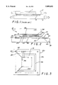
- FIG. 2 shows an electronic assembly 10 of the present invention.
- the assembly 10 includes an integrated circuit package 12 that is mounted to a printed circuit board 14.
- the integrated circuit package 12 includes an integrated circuit 16 that is mounted to a bond portion 18 of a substrate 20.
- the substrate 20 has a first side 22 and an opposite second side 24.
- the integrated circuit 16 may be a microprocessor, although it is to be understood that the package 12 may contain any electrical device.
- the substrate 20 has a contact portion 26 that is separated from the bond portion 18 by a flexible portion 28.
- the contact portion 26 has a plurality of contact pads 30 that are located on the second side 24 of the substrate 20.
- the contact pads 30 are connected to a plurality of conductive traces 32 by a plurality of vias 34 that extend through the substrate 20.
- the conductive traces 32 are routed to a plurality of bond pads 36 located in the bond portion 18 of the substrate 20.
- the integrated circuit 16 may be mounted to the substrate 20 by solder bumps 38 that are attached to the bond pads 36 with a process commonly referred to as C4 or "flip chip". Although it is to be understood that the integrated circuit 16 can be mounted to the substrate 20 by other means such as wire bonds, or tape automated bonding (TAB).
- the substrate 20 is mounted to the printed circuit board 14 by solder joints 40 that attach the contact pads 30 to corresponding surface pads (not shown) of the circuit board 14.
- the package 12 and the circuit board 14 undergo a thermal expansion.
- the package 12 and board 14 have different coefficients of thermal expansion which produce different expansion rates.
- the flexible portion 28 mechanically decouples the contact portion 26 from the bond portion 18 so that the integrated circuit 16 and connected bond portion 18 can move relative to the circuit board 14 and connected contact portion 26. The relative movement minimizes the strain and corresponding stress on the solder joints 40 and solder bumps 38.
- the package 12 may also have a heat conductive member 42 that is coupled to the integrated circuit 16.
- the heat conductive member 42 may be a heat pipe, heat sink, heat slug, etc., which efficiently removes heat generated by the integrated circuit 16.
- the heat conductive member 42 is clamped onto the integrated circuit 16 by a clamp (not shown).
- the heat conductive member 42 is separated from the integrated circuit 16 by a spacer 44.
- the spacer 44 may be an O-ring or a pair of plastic pieces that are flexible enough to conform to irregularities in the surfaces of the devices 16 and 42 and more uniformly distribute the clamping force from the member 42 to the circuit 16.
- a thermally conductive material such as a thermal grease or a thermal epoxy 46 may fill the space between the integrated circuit 16 and the conductive member 42.
- the thermal grease or epoxy provides a thermal path of relatively low impedance between the two devices 16 and 42.
- the spacer 44 also provides a means to accurately control the thickness of the thermal grease or epoxy 46.
- An elastomer 48 may be located between the bond portion 18 of the substrate 20 and the printed circuit board 14.
- the elastomer 48 supports the bond portion 18 and compensates for tolerances between the package 12 and the clamp of the heat conductive member 42.
- the elastomer 48 may be conductive to provide an electrical path between the substrate 20 and the printed circuit board 14.
- the package 12 may be assembled by initially building the substrate 20.
- the substrate 20 may include a top layer of flexible material 50 that is attached to a pair of rigid substrates 52 and 54 that define the bond 18 and contact 26 portions, respectively.
- the flexible material 50 may be a polyimide material commonly sold under the trademark KAPTON which has the bond pads 36 and conductive traces 32 formed on a surface of the polyimide.
- the rigid substrate 54 for the contact portion may have the contact pads 30 formed on a surface of the substrate 54.
- the flexible polyimide 50 may be bonded to the rigid substrates 52 and 54 with conventional autoclave processes.
- the vias 34 may then be formed to connect the traces 32 to the contact pads 30.
- the integrated circuit 16 may be mounted to the substrate 20 with conventional C4 processes. Solder balls may be attached to the contact pads 30 and then mounted onto the corresponding surface pads of the printed circuit board 14. Alternatively, a solder paste may be screened onto the contact pads 30 or printed circuit board 14. The elastomer 48 is placed onto the printed circuit board 14 before the package 12 is mounted to the board 14. The solder is heated and reflowed to create the solder joints 40 that attach the substrate 20 to the board 14. The solder can be reflowed with an induction bar (not shown) that is placed onto the contact portion 26 of the substrate 20.
- the spacer 44 is placed onto the integrated circuit 16 so that there is a cavity on top of the circuit 16.
- the thermal grease or epoxy 46 is then dispensed onto the integrated circuit 16 to fill the cavity.
- the heat conductive member 42 can then be clamped onto the spacer 44 to complete the electronic assembly 10. It is to be understood that the order of the process steps may be varied. For example, the thermal grease or epoxy 46 may be applied after the substrate 20 is attached to the printed circuit board 14.
Abstract
An integrated circuit package that contains an integrated circuit that is mounted to a bond portion of a substrate. The bond portion of the substrate is separated from a contact portion of the substrate by a flexible portion. The contact portion is attached to a printed circuit board by a plurality of solder joints. The flexible portion decouples the bond portion from the contact portion to allow relative movement between the package and the circuit board to minimize the strain on the solder joints. The package may also contain a spacer that separates a heat pipe from the integrated circuit and controls the thickness of a thermal grease located between the circuit and the pipe.
Description
1. Field of the Invention
The present invention relates to an integrated circuit package.
2. Description of Related Art
As shown in FIG. 1, an integrated circuit 1 is typically assembled into a package 2 that is soldered to a printed circuit board 3. The package 2 is attached to the board 3 by a plurality of solder joints 4. The integrated circuit package 2 and printed circuit board 3 are typically utilized in an environment which has a varying ambient temperature. A variation in the integrated circuit package temperature will create a different thermal expansion rate between the integrated circuit package 2 and the printed circuit board 3.
The integrated circuit 1 and package 2 have a composite coefficient of thermal expansion (CTE) that is different than the coefficient of expansion of the circuit board 3. Consequently, the package 2 undergoes a different rate of thermal expansion than the circuit board as indicated in phantom on the drawing. This difference in expansion rate produces a strain in the solder joints. When cycled over time it has been found that the mechanical strain may crack the solder joint(s) and create an electrical open between the package 2 and the board 3. It would be desirable to provide an integrated circuit package that compensates for the different CTEs of the package and a printed circuit board to minimize the strain on the solder joints.
Some integrated circuits generate a relatively large amount of heat that must be removed from the package. To minimize the circuit junction temperatures there have been incorporated into the packages various heat conductive members that increase the heat transfer rate from the integrated circuit and the package. The heat conductive member may be a heat pipe that is clamped to the integrated circuit. The clamping force of the heat pipe may create localized stresses that crack and damage the integrated circuit. It would be desirable to have an integrated circuit package that can effectively couple a heat conductive member to an integrated circuit while providing an efficient thermal path between the two devices.
The present invention is an integrated circuit package that contains an integrated circuit that is mounted to a bond portion of a substrate. The bond portion of the substrate is separated from a contact portion of the substrate by a flexible portion.
FIG. 1 is a cross-sectional view of an electronic assembly of the prior art;
FIG. 2 is a cross-sectional view of an electronic assembly of the present invention;
FIG. 3 is a top view of a substrate of the package.
The present invention is an integrated circuit package that contains an integrated circuit which is mounted to a bond portion of a substrate. The bond portion of the substrate is separated from a contact portion of the substrate by a flexible portion. The contact portion is attached to a printed circuit board by a plurality of solder joints. The flexible portion decouples the bond portion from the contact portion to allow relative movement between the package and the circuit board. The relative movement minimizes the strain on the solder joints when the assembly undergoes thermal expansion, or is subjected to external shock and vibration loads. The package may also contain a spacer that separates a heat pipe from the integrated circuit and controls the thickness of a thermal grease located between the circuit and the pipe. The spacer more uniformly distributes the clamping force of the heat pipe on the integrated circuit.
Referring to the drawings more particularly by reference numbers, FIG. 2 shows an electronic assembly 10 of the present invention. The assembly 10 includes an integrated circuit package 12 that is mounted to a printed circuit board 14. The integrated circuit package 12 includes an integrated circuit 16 that is mounted to a bond portion 18 of a substrate 20. The substrate 20 has a first side 22 and an opposite second side 24. The integrated circuit 16 may be a microprocessor, although it is to be understood that the package 12 may contain any electrical device.
As shown in FIG. 3, the substrate 20 has a contact portion 26 that is separated from the bond portion 18 by a flexible portion 28. The contact portion 26 has a plurality of contact pads 30 that are located on the second side 24 of the substrate 20. The contact pads 30 are connected to a plurality of conductive traces 32 by a plurality of vias 34 that extend through the substrate 20. The conductive traces 32 are routed to a plurality of bond pads 36 located in the bond portion 18 of the substrate 20.
Referring to FIG. 2, the integrated circuit 16 may be mounted to the substrate 20 by solder bumps 38 that are attached to the bond pads 36 with a process commonly referred to as C4 or "flip chip". Although it is to be understood that the integrated circuit 16 can be mounted to the substrate 20 by other means such as wire bonds, or tape automated bonding (TAB). The substrate 20 is mounted to the printed circuit board 14 by solder joints 40 that attach the contact pads 30 to corresponding surface pads (not shown) of the circuit board 14.
When the temperature of the assembly varies, the package 12 and the circuit board 14 undergo a thermal expansion. The package 12 and board 14 have different coefficients of thermal expansion which produce different expansion rates. The flexible portion 28 mechanically decouples the contact portion 26 from the bond portion 18 so that the integrated circuit 16 and connected bond portion 18 can move relative to the circuit board 14 and connected contact portion 26. The relative movement minimizes the strain and corresponding stress on the solder joints 40 and solder bumps 38.
The package 12 may also have a heat conductive member 42 that is coupled to the integrated circuit 16. The heat conductive member 42 may be a heat pipe, heat sink, heat slug, etc., which efficiently removes heat generated by the integrated circuit 16. The heat conductive member 42 is clamped onto the integrated circuit 16 by a clamp (not shown).
The heat conductive member 42 is separated from the integrated circuit 16 by a spacer 44. The spacer 44 may be an O-ring or a pair of plastic pieces that are flexible enough to conform to irregularities in the surfaces of the devices 16 and 42 and more uniformly distribute the clamping force from the member 42 to the circuit 16.
A thermally conductive material such as a thermal grease or a thermal epoxy 46 may fill the space between the integrated circuit 16 and the conductive member 42. The thermal grease or epoxy provides a thermal path of relatively low impedance between the two devices 16 and 42. The spacer 44 also provides a means to accurately control the thickness of the thermal grease or epoxy 46.
An elastomer 48 may be located between the bond portion 18 of the substrate 20 and the printed circuit board 14. The elastomer 48 supports the bond portion 18 and compensates for tolerances between the package 12 and the clamp of the heat conductive member 42. The elastomer 48 may be conductive to provide an electrical path between the substrate 20 and the printed circuit board 14.
The package 12 may be assembled by initially building the substrate 20. The substrate 20 may include a top layer of flexible material 50 that is attached to a pair of rigid substrates 52 and 54 that define the bond 18 and contact 26 portions, respectively. The flexible material 50 may be a polyimide material commonly sold under the trademark KAPTON which has the bond pads 36 and conductive traces 32 formed on a surface of the polyimide. The rigid substrate 54 for the contact portion may have the contact pads 30 formed on a surface of the substrate 54. The flexible polyimide 50 may be bonded to the rigid substrates 52 and 54 with conventional autoclave processes. The vias 34 may then be formed to connect the traces 32 to the contact pads 30.
The integrated circuit 16 may be mounted to the substrate 20 with conventional C4 processes. Solder balls may be attached to the contact pads 30 and then mounted onto the corresponding surface pads of the printed circuit board 14. Alternatively, a solder paste may be screened onto the contact pads 30 or printed circuit board 14. The elastomer 48 is placed onto the printed circuit board 14 before the package 12 is mounted to the board 14. The solder is heated and reflowed to create the solder joints 40 that attach the substrate 20 to the board 14. The solder can be reflowed with an induction bar (not shown) that is placed onto the contact portion 26 of the substrate 20.
The spacer 44 is placed onto the integrated circuit 16 so that there is a cavity on top of the circuit 16. The thermal grease or epoxy 46 is then dispensed onto the integrated circuit 16 to fill the cavity. The heat conductive member 42 can then be clamped onto the spacer 44 to complete the electronic assembly 10. It is to be understood that the order of the process steps may be varied. For example, the thermal grease or epoxy 46 may be applied after the substrate 20 is attached to the printed circuit board 14.
What is thus provided is an integrated circuit package that allows relative movement between the package and an attached printed circuit board, and provides a means to mechanically connect a heat conductive member while controlling a thickness of a thermal grease or epoxy.
Claims (11)
1. An integrated circuit package, comprising:
a flexible circuit board which has a bond portion and a contact portion;
a center substrate that is attached to said bond portion of said flexible circuit board;
an end substrate that is attached to said contact portion of said flexible circuit board; and,
an integrated circuit that is mounted to said bond portion of said flexible circuit board.
2. The package as recited in claim 1, wherein said contact portion has a plurality of contact pads.
3. The package as recited in claim 1, wherein said integrated circuit is mounted to said bond portion by a plurality of solder bumps.
4. The package as recited in claim 1, further comprising a heat pipe that is coupled to said integrated circuit.
5. The package as recited in claim 4, further comprising a spacer that separates said heat pipe from said integrated circuit.
6. The package as recited in claim 5, further comprising a thermal grease located between said integrated circuit and said heat pipe.
7. The package as recited in claim 1, further comprising a printed circuit board that is attached to said end substrate and an elastomer located between said center substrate and said printed circuit board.
8. An electronic assembly, comprising:
a substrate that has a rigid bond portion that is separated from a rigid contact portion by a flexible portion of said substrate;
an integrated circuit that is mounted to said rigid bond portion of said substrate;
a heat conductive member that is coupled to said integrated circuit;
a spacer that separates said heat conductive member from said integrated circuit;
a printed circuit board that is attached to said contact portion of said substrate;
an elastomer that separates said bond portion of said substrate from said printed circuit board.
9. The assembly as recited in claim 8, wherein said rigid contact portion has a plurality of contact pads.
10. The assembly as recited in claim 8, wherein said integrated circuit is mounted to said bond portion by a plurality of solder bumps.
11. The assembly as recited in claim 10, wherein said heat conductive member is a heat pipe.
Priority Applications (2)
| Application Number | Priority Date | Filing Date | Title |
|---|---|---|---|
| US08/837,596 US5889652A (en) | 1997-04-21 | 1997-04-21 | C4-GT stand off rigid flex interposer |
| US09/198,438 US6088915A (en) | 1997-04-21 | 1998-11-24 | C4-GT stand off rigid flex interposer method |
Applications Claiming Priority (1)
| Application Number | Priority Date | Filing Date | Title |
|---|---|---|---|
| US08/837,596 US5889652A (en) | 1997-04-21 | 1997-04-21 | C4-GT stand off rigid flex interposer |
Related Child Applications (1)
| Application Number | Title | Priority Date | Filing Date |
|---|---|---|---|
| US09/198,438 Division US6088915A (en) | 1997-04-21 | 1998-11-24 | C4-GT stand off rigid flex interposer method |
Publications (1)
| Publication Number | Publication Date |
|---|---|
| US5889652A true US5889652A (en) | 1999-03-30 |
Family
ID=25274912
Family Applications (2)
| Application Number | Title | Priority Date | Filing Date |
|---|---|---|---|
| US08/837,596 Expired - Fee Related US5889652A (en) | 1997-04-21 | 1997-04-21 | C4-GT stand off rigid flex interposer |
| US09/198,438 Expired - Lifetime US6088915A (en) | 1997-04-21 | 1998-11-24 | C4-GT stand off rigid flex interposer method |
Family Applications After (1)
| Application Number | Title | Priority Date | Filing Date |
|---|---|---|---|
| US09/198,438 Expired - Lifetime US6088915A (en) | 1997-04-21 | 1998-11-24 | C4-GT stand off rigid flex interposer method |
Country Status (1)
| Country | Link |
|---|---|
| US (2) | US5889652A (en) |
Cited By (21)
| Publication number | Priority date | Publication date | Assignee | Title |
|---|---|---|---|---|
| US6218730B1 (en) * | 1999-01-06 | 2001-04-17 | International Business Machines Corporation | Apparatus for controlling thermal interface gap distance |
| US6392887B1 (en) | 1999-12-14 | 2002-05-21 | Intel Corporation | PLGA-BGA socket using elastomer connectors |
| US20020137252A1 (en) * | 2001-03-21 | 2002-09-26 | Larson Charles E. | Folded interposer |
| US20030116860A1 (en) * | 2001-12-21 | 2003-06-26 | Biju Chandran | Semiconductor package with low resistance package-to-die interconnect scheme for reduced die stresses |
| US6631078B2 (en) * | 2002-01-10 | 2003-10-07 | International Business Machines Corporation | Electronic package with thermally conductive standoff |
| US6775150B1 (en) | 2000-08-30 | 2004-08-10 | Intel Corporation | Electronic assembly comprising ceramic/organic hybrid substrate with embedded capacitors and methods of manufacture |
| US6809935B1 (en) | 2000-10-10 | 2004-10-26 | Megic Corporation | Thermally compliant PCB substrate for the application of chip scale packages |
| GB2403070A (en) * | 2003-06-16 | 2004-12-22 | Uniwill Comp Corp | An element for retaining thermal interface material used with electronic components |
| US20040262778A1 (en) * | 2003-06-30 | 2004-12-30 | Fay Hua | Electromigration barrier layers for solder joints |
| US6846115B1 (en) | 2001-01-29 | 2005-01-25 | Jds Uniphase Corporation | Methods, apparatus, and systems of fiber optic modules, elastomeric connections, and retention mechanisms therefor |
| US20050133907A1 (en) * | 2003-12-23 | 2005-06-23 | Hildner Thomas R. | Mechanism for maintaining consistent thermal interface layer in an integrated circuit assembly |
| US6970362B1 (en) | 2000-07-31 | 2005-11-29 | Intel Corporation | Electronic assemblies and systems comprising interposer with embedded capacitors |
| US7032392B2 (en) * | 2001-12-19 | 2006-04-25 | Intel Corporation | Method and apparatus for cooling an integrated circuit package using a cooling fluid |
| US20060102323A1 (en) * | 2003-02-14 | 2006-05-18 | Prosenjit Ghosh | Radially shaped heat pipe |
| EP1300883A3 (en) * | 2001-10-04 | 2007-01-10 | Delphi Technologies, Inc. | Thermal dissipation assembly for electronic components |
| US7235886B1 (en) | 2001-12-21 | 2007-06-26 | Intel Corporation | Chip-join process to reduce elongation mismatch between the adherents and semiconductor package made thereby |
| US20070222064A1 (en) * | 2005-07-19 | 2007-09-27 | Edwards David L | Thermal paste containment for semiconductor modules |
| US20080293261A1 (en) * | 2007-03-28 | 2008-11-27 | Ixys Seminconductor Gmbh | Arrangement of at least one power semiconductor module and a printed circuit board |
| US20090085199A1 (en) * | 2007-09-30 | 2009-04-02 | In Sang Yoon | Integrated circuit package system with mold lock subassembly |
| US20090321898A1 (en) * | 2008-06-25 | 2009-12-31 | Reza Argenty Pagaila | Conformal shielding integrated circuit package system |
| US20120020040A1 (en) * | 2010-07-26 | 2012-01-26 | Lin Paul T | Package-to-package stacking by using interposer with traces, and or standoffs and solder balls |
Families Citing this family (10)
| Publication number | Priority date | Publication date | Assignee | Title |
|---|---|---|---|---|
| US6046496A (en) | 1997-11-04 | 2000-04-04 | Micron Technology Inc | Chip package |
| US6335491B1 (en) * | 2000-02-08 | 2002-01-01 | Lsi Logic Corporation | Interposer for semiconductor package assembly |
| US6992887B2 (en) * | 2003-10-15 | 2006-01-31 | Visteon Global Technologies, Inc. | Liquid cooled semiconductor device |
| JP4303609B2 (en) * | 2004-01-29 | 2009-07-29 | 富士通株式会社 | Spacer |
| US20060185836A1 (en) * | 2005-02-24 | 2006-08-24 | Scott Garner | Thermally coupled surfaces having controlled minimum clearance |
| US7475718B2 (en) * | 2006-11-15 | 2009-01-13 | Delphi Technologies, Inc. | Orientation insensitive multi chamber thermosiphon |
| US20090110345A1 (en) * | 2007-10-26 | 2009-04-30 | International Business Machines Corporation | Methods for passive micrometer-range alignment of components using removable reference structures |
| US7961469B2 (en) * | 2009-03-31 | 2011-06-14 | Apple Inc. | Method and apparatus for distributing a thermal interface material |
| JP5636908B2 (en) * | 2010-11-24 | 2014-12-10 | 富士通株式会社 | Socket and electronic device |
| FR3023975A1 (en) * | 2014-07-18 | 2016-01-22 | Thales Sa | THERMAL INTERFACE DEVICE WITH MICROPOROUS SEAL CAPABLE OF PREVENTING MIGRATION OF THERMAL GREASE |
Citations (9)
| Publication number | Priority date | Publication date | Assignee | Title |
|---|---|---|---|---|
| US3626252A (en) * | 1970-01-21 | 1971-12-07 | Keithley Instruments | Temperature equalization for printed circuits |
| US5311060A (en) * | 1989-12-19 | 1994-05-10 | Lsi Logic Corporation | Heat sink for semiconductor device assembly |
| US5467251A (en) * | 1993-10-08 | 1995-11-14 | Northern Telecom Limited | Printed circuit boards and heat sink structures |
| US5532906A (en) * | 1992-09-14 | 1996-07-02 | Kabushiki Kaisha Toshiba | Wiring substrate |
| US5550406A (en) * | 1992-06-04 | 1996-08-27 | Lsi Logic Corporation | Multi-layer tab tape having distinct signal, power and ground planes and wafer probe card with multi-layer substrate |
| US5572407A (en) * | 1994-07-22 | 1996-11-05 | Hughes Aircraft Company | Apparatus for interconnecting an integrated circuit device to a multilayer printed wiring board |
| US5586010A (en) * | 1995-03-13 | 1996-12-17 | Texas Instruments Incorporated | Low stress ball grid array package |
| US5672548A (en) * | 1994-07-11 | 1997-09-30 | International Business Machines Corporation | Method for attaching heat sinks directly to chip carrier modules using flexible-epoxy |
| US5706171A (en) * | 1995-11-20 | 1998-01-06 | International Business Machines Corporation | Flat plate cooling using a thermal paste retainer |
Family Cites Families (4)
| Publication number | Priority date | Publication date | Assignee | Title |
|---|---|---|---|---|
| US4092697A (en) * | 1976-12-06 | 1978-05-30 | International Business Machines Corporation | Heat transfer mechanism for integrated circuit package |
| US4561011A (en) * | 1982-10-05 | 1985-12-24 | Mitsubishi Denki Kabushiki Kaisha | Dimensionally stable semiconductor device |
| JP3018554B2 (en) * | 1991-04-25 | 2000-03-13 | 株式会社日立製作所 | Semiconductor module and method of manufacturing the same |
| US5585671A (en) * | 1994-10-07 | 1996-12-17 | Nagesh; Voddarahalli K. | Reliable low thermal resistance package for high power flip clip ICs |
-
1997
- 1997-04-21 US US08/837,596 patent/US5889652A/en not_active Expired - Fee Related
-
1998
- 1998-11-24 US US09/198,438 patent/US6088915A/en not_active Expired - Lifetime
Patent Citations (10)
| Publication number | Priority date | Publication date | Assignee | Title |
|---|---|---|---|---|
| US3626252A (en) * | 1970-01-21 | 1971-12-07 | Keithley Instruments | Temperature equalization for printed circuits |
| US5311060A (en) * | 1989-12-19 | 1994-05-10 | Lsi Logic Corporation | Heat sink for semiconductor device assembly |
| US5550406A (en) * | 1992-06-04 | 1996-08-27 | Lsi Logic Corporation | Multi-layer tab tape having distinct signal, power and ground planes and wafer probe card with multi-layer substrate |
| US5532906A (en) * | 1992-09-14 | 1996-07-02 | Kabushiki Kaisha Toshiba | Wiring substrate |
| US5467251A (en) * | 1993-10-08 | 1995-11-14 | Northern Telecom Limited | Printed circuit boards and heat sink structures |
| US5672548A (en) * | 1994-07-11 | 1997-09-30 | International Business Machines Corporation | Method for attaching heat sinks directly to chip carrier modules using flexible-epoxy |
| US5744863A (en) * | 1994-07-11 | 1998-04-28 | International Business Machines Corporation | Chip carrier modules with heat sinks attached by flexible-epoxy |
| US5572407A (en) * | 1994-07-22 | 1996-11-05 | Hughes Aircraft Company | Apparatus for interconnecting an integrated circuit device to a multilayer printed wiring board |
| US5586010A (en) * | 1995-03-13 | 1996-12-17 | Texas Instruments Incorporated | Low stress ball grid array package |
| US5706171A (en) * | 1995-11-20 | 1998-01-06 | International Business Machines Corporation | Flat plate cooling using a thermal paste retainer |
Cited By (42)
| Publication number | Priority date | Publication date | Assignee | Title |
|---|---|---|---|---|
| US6218730B1 (en) * | 1999-01-06 | 2001-04-17 | International Business Machines Corporation | Apparatus for controlling thermal interface gap distance |
| US6392887B1 (en) | 1999-12-14 | 2002-05-21 | Intel Corporation | PLGA-BGA socket using elastomer connectors |
| US7339798B2 (en) | 2000-07-31 | 2008-03-04 | Intel Corporation | Electronic assemblies and systems comprising interposer with embedded capacitors |
| US20060012966A1 (en) * | 2000-07-31 | 2006-01-19 | Intel Corporation | Electronic assemblies and systems comprising interposer with embedded capacitors |
| US6970362B1 (en) | 2000-07-31 | 2005-11-29 | Intel Corporation | Electronic assemblies and systems comprising interposer with embedded capacitors |
| US6775150B1 (en) | 2000-08-30 | 2004-08-10 | Intel Corporation | Electronic assembly comprising ceramic/organic hybrid substrate with embedded capacitors and methods of manufacture |
| US7120031B2 (en) | 2000-08-30 | 2006-10-10 | Intel Corporation | Data processing system comprising ceramic/organic hybrid substrate with embedded capacitors |
| US20040238942A1 (en) * | 2000-08-30 | 2004-12-02 | Intel Corporation | Electronic assembly comprising ceramic/organic hybrid substrate with embedded capacitors and methods of manufacture |
| US7535728B2 (en) | 2000-08-30 | 2009-05-19 | Intel Corporation | Electronic assemblies comprising ceramic/organic hybrid substrate with embedded capacitors |
| US20060279940A1 (en) * | 2000-08-30 | 2006-12-14 | Intel Corporation | Electronic assemblies comprising ceramic/organic hybrid substrate with embedded capacitors |
| US6809935B1 (en) | 2000-10-10 | 2004-10-26 | Megic Corporation | Thermally compliant PCB substrate for the application of chip scale packages |
| US6846115B1 (en) | 2001-01-29 | 2005-01-25 | Jds Uniphase Corporation | Methods, apparatus, and systems of fiber optic modules, elastomeric connections, and retention mechanisms therefor |
| US6884653B2 (en) | 2001-03-21 | 2005-04-26 | Micron Technology, Inc. | Folded interposer |
| US20060242477A1 (en) * | 2001-03-21 | 2006-10-26 | Larson Charles E | Folded interposer |
| US20020137252A1 (en) * | 2001-03-21 | 2002-09-26 | Larson Charles E. | Folded interposer |
| US6982869B2 (en) | 2001-03-21 | 2006-01-03 | Micron Technology, Inc. | Folded interposer |
| US20030062614A1 (en) * | 2001-03-21 | 2003-04-03 | Larson Charles E. | Folded interposer |
| EP1300883A3 (en) * | 2001-10-04 | 2007-01-10 | Delphi Technologies, Inc. | Thermal dissipation assembly for electronic components |
| US7032392B2 (en) * | 2001-12-19 | 2006-04-25 | Intel Corporation | Method and apparatus for cooling an integrated circuit package using a cooling fluid |
| US7235886B1 (en) | 2001-12-21 | 2007-06-26 | Intel Corporation | Chip-join process to reduce elongation mismatch between the adherents and semiconductor package made thereby |
| US20030116860A1 (en) * | 2001-12-21 | 2003-06-26 | Biju Chandran | Semiconductor package with low resistance package-to-die interconnect scheme for reduced die stresses |
| US20050116329A1 (en) * | 2001-12-21 | 2005-06-02 | Intel Corporation | Semiconductor package with low resistance package-to-die interconnect scheme for reduced die stresses |
| US7122403B2 (en) | 2001-12-21 | 2006-10-17 | Intel Corporation | Method of interconnecting die and substrate |
| US6631078B2 (en) * | 2002-01-10 | 2003-10-07 | International Business Machines Corporation | Electronic package with thermally conductive standoff |
| US20060102323A1 (en) * | 2003-02-14 | 2006-05-18 | Prosenjit Ghosh | Radially shaped heat pipe |
| GB2403070A (en) * | 2003-06-16 | 2004-12-22 | Uniwill Comp Corp | An element for retaining thermal interface material used with electronic components |
| GB2403070B (en) * | 2003-06-16 | 2005-08-17 | Uniwill Comp Corp | A structure for containing thermal interface material in electrical equipment |
| US7242097B2 (en) | 2003-06-30 | 2007-07-10 | Intel Corporation | Electromigration barrier layers for solder joints |
| US20040262778A1 (en) * | 2003-06-30 | 2004-12-30 | Fay Hua | Electromigration barrier layers for solder joints |
| US7122460B2 (en) | 2003-06-30 | 2006-10-17 | Intel Corporation | Electromigration barrier layers for solder joints |
| US20050133907A1 (en) * | 2003-12-23 | 2005-06-23 | Hildner Thomas R. | Mechanism for maintaining consistent thermal interface layer in an integrated circuit assembly |
| US20070222064A1 (en) * | 2005-07-19 | 2007-09-27 | Edwards David L | Thermal paste containment for semiconductor modules |
| US8531025B2 (en) | 2005-07-19 | 2013-09-10 | International Business Machines Corporation | Thermal paste containment for semiconductor modules |
| US7780469B2 (en) * | 2007-03-28 | 2010-08-24 | Ixys Ch Gmbh | Arrangement of at least one power semiconductor module and a printed circuit board |
| US20080293261A1 (en) * | 2007-03-28 | 2008-11-27 | Ixys Seminconductor Gmbh | Arrangement of at least one power semiconductor module and a printed circuit board |
| US20080299707A1 (en) * | 2007-05-30 | 2008-12-04 | International Business Machines Corporation | Thermal paste containment for semiconductor modules |
| US8021925B2 (en) * | 2007-05-30 | 2011-09-20 | International Business Machines Corporation | Thermal paste containment for semiconductor modules |
| US20090085199A1 (en) * | 2007-09-30 | 2009-04-02 | In Sang Yoon | Integrated circuit package system with mold lock subassembly |
| US7667314B2 (en) | 2007-09-30 | 2010-02-23 | Stats Chippac Ltd. | Integrated circuit package system with mold lock subassembly |
| US20090321898A1 (en) * | 2008-06-25 | 2009-12-31 | Reza Argenty Pagaila | Conformal shielding integrated circuit package system |
| US7968979B2 (en) | 2008-06-25 | 2011-06-28 | Stats Chippac Ltd. | Integrated circuit package system with conformal shielding and method of manufacture thereof |
| US20120020040A1 (en) * | 2010-07-26 | 2012-01-26 | Lin Paul T | Package-to-package stacking by using interposer with traces, and or standoffs and solder balls |
Also Published As
| Publication number | Publication date |
|---|---|
| US6088915A (en) | 2000-07-18 |
Similar Documents
| Publication | Publication Date | Title |
|---|---|---|
| US5889652A (en) | C4-GT stand off rigid flex interposer | |
| US5956235A (en) | Method and apparatus for flexibly connecting electronic devices | |
| US6224711B1 (en) | Assembly process for flip chip package having a low stress chip and resulting structure | |
| US5639696A (en) | Microelectronic integrated circuit mounted on circuit board with solder column grid array interconnection, and method of fabricating the solder column grid array | |
| KR100314974B1 (en) | Method and apparatus for insulating moisture sensitive pbga's | |
| US6046910A (en) | Microelectronic assembly having slidable contacts and method for manufacturing the assembly | |
| US5811317A (en) | Process for reflow bonding a semiconductor die to a substrate and the product produced by the product | |
| JP3368177B2 (en) | Apparatus and method for providing effective heat sink contact to structural elements of a substrate | |
| US6458623B1 (en) | Conductive adhesive interconnection with insulating polymer carrier | |
| US6963033B2 (en) | Ball grid array attaching means having improved reliability and method of manufacturing same | |
| WO1994018701A1 (en) | Stress-resistant semiconductor chip-circuit board interconnect | |
| US6927095B2 (en) | Low cost and compliant microelectronic packages for high I/O and fine pitch | |
| US5761048A (en) | Conductive polymer ball attachment for grid array semiconductor packages | |
| US5844319A (en) | Microelectronic assembly with collar surrounding integrated circuit component on a substrate | |
| KR20010105415A (en) | Mounting structure for semiconductor chip, semiconductor device, and method of manufacturing semiconductor device | |
| EP0838100B1 (en) | Separable electrical connector assembly having a planar array of conductive protrusions | |
| US6657313B1 (en) | Dielectric interposer for chip to substrate soldering | |
| US6413849B1 (en) | Integrated circuit package with surface mounted pins on an organic substrate and method of fabrication therefor | |
| US6757968B2 (en) | Chip scale packaging on CTE matched printed wiring boards | |
| US7719108B2 (en) | Enhanced reliability semiconductor package | |
| JP2570468B2 (en) | Manufacturing method of LSI module | |
| JP2008210842A (en) | Mounting method of electronic component with bump | |
| EP1317001A1 (en) | A semiconductor device | |
| JPH1197569A (en) | Semiconductor package | |
| WO2002023963A2 (en) | Method and apparatus for surface mounting electrical devices |
Legal Events
| Date | Code | Title | Description |
|---|---|---|---|
| AS | Assignment |
Owner name: INTEL CORPORATION, CALIFORNIA Free format text: ASSIGNMENT OF ASSIGNORS INTEREST;ASSIGNOR:TURTURRO, GREGORY;REEL/FRAME:008530/0598 Effective date: 19970416 |
|
| FPAY | Fee payment |
Year of fee payment: 4 |
|
| REMI | Maintenance fee reminder mailed | ||
| FPAY | Fee payment |
Year of fee payment: 8 |
|
| REMI | Maintenance fee reminder mailed | ||
| LAPS | Lapse for failure to pay maintenance fees | ||
| STCH | Information on status: patent discontinuation |
Free format text: PATENT EXPIRED DUE TO NONPAYMENT OF MAINTENANCE FEES UNDER 37 CFR 1.362 |
|
| FP | Lapsed due to failure to pay maintenance fee |
Effective date: 20110330 |