US5894234A - Differential comparator with fixed and controllable hysteresis - Google Patents
Differential comparator with fixed and controllable hysteresis Download PDFInfo
- Publication number
- US5894234A US5894234A US08/846,390 US84639097A US5894234A US 5894234 A US5894234 A US 5894234A US 84639097 A US84639097 A US 84639097A US 5894234 A US5894234 A US 5894234A
- Authority
- US
- United States
- Prior art keywords
- comparator
- passive
- input
- output
- offset
- Prior art date
- Legal status (The legal status is an assumption and is not a legal conclusion. Google has not performed a legal analysis and makes no representation as to the accuracy of the status listed.)
- Expired - Lifetime
Links
Images

Classifications
-
- H—ELECTRICITY
- H03—ELECTRONIC CIRCUITRY
- H03K—PULSE TECHNIQUE
- H03K5/00—Manipulating of pulses not covered by one of the other main groups of this subclass
- H03K5/22—Circuits having more than one input and one output for comparing pulses or pulse trains with each other according to input signal characteristics, e.g. slope, integral
- H03K5/24—Circuits having more than one input and one output for comparing pulses or pulse trains with each other according to input signal characteristics, e.g. slope, integral the characteristic being amplitude
- H03K5/2472—Circuits having more than one input and one output for comparing pulses or pulse trains with each other according to input signal characteristics, e.g. slope, integral the characteristic being amplitude using field effect transistors
- H03K5/2481—Circuits having more than one input and one output for comparing pulses or pulse trains with each other according to input signal characteristics, e.g. slope, integral the characteristic being amplitude using field effect transistors with at least one differential stage
-
- H—ELECTRICITY
- H03—ELECTRONIC CIRCUITRY
- H03K—PULSE TECHNIQUE
- H03K3/00—Circuits for generating electric pulses; Monostable, bistable or multistable circuits
- H03K3/02—Generators characterised by the type of circuit or by the means used for producing pulses
- H03K3/353—Generators characterised by the type of circuit or by the means used for producing pulses by the use, as active elements, of field-effect transistors with internal or external positive feedback
- H03K3/356—Bistable circuits
- H03K3/3565—Bistables with hysteresis, e.g. Schmitt trigger
Definitions
- the present invention relates to electrical circuitry, and, in particular, to differential comparators.
- a differential comparator is an electrical circuit that compares two input voltages and generates an output voltage that indicates the relationship between the two inputs. For example, for a particular differential comparator, when the first input voltage is greater than the second input voltage, the output voltage from the differential comparator will be high. Similarly, when the first input voltage is less than the second input voltage, the output voltage will be low. Thus, the output voltage may be used to indicate which input voltage is greater.
- an application may need to determine whether or not the first input voltage is greater than the sum of the second input voltage and an offset voltage.
- An offset voltage is said to be fixed, if its value can be maintained as a constant for one or more comparison operations.
- an offset voltage is said to be controllable, if its value can be selectively changed for different comparison operations.
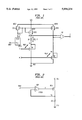
- FIG. 1 shows a schematic diagram of a conventional differential comparator 100 having a fixed and controllable offset voltage.
- Comparator 100 has a current source X1 whose current ICS1 is mirrored by transistor MCS1 through transistors MCS2 and MCS3 to produce currents ICS2 and ICS3, respectively.
- FIG. 2 shows a schematic diagram of current source X1 of FIG. 1.
- a controllable reference voltage VREF is applied to the positive input of an operational amplifier (op-amp) OPCS1.
- the negative input comes from node FB, which is connected between a reference resistor RCS and the source of an N-channel transistors MFB.
- the output of the op-amp OPCS1 goes to the gate of transistor MFB. In this manner, the voltage at node FB is forced to be equal to VREF, so that the current through transistor MFB is equal to VREF/RCS (i.e., ICS1 of FIG. 1).
- differential comparator 100 the inputs to differential comparator 100 are applied at nodes P and N, which are in turn applied to the gates of P-channel transistors M1 and M2, respectively. If the current densities through transistors M1 and M2 are kept equal, then the gate-to-source voltages VGS will be equal in M1 and M2. Node P1 will then be at voltage P+VGS1, while node N1 will be at voltage P+VGS2.
- resistors RIP and RCS are made on a single integrated circuit from the same material (e.g., N-tub, P+ source-drain), then the ratio of RP/RCS is a constant fixed by the geometric layout. Similarly, the ratio MCS2/MCS1 is also fixed by geometry (i.e., the transistor channel widths). Thus, the voltage drop De1V across resistor RP is directly proportional to the reference voltage VREF.
- Comparator X2 is a low-offset comparator in that it has low or negligible offset (e.g., typically less than 10 mvolts). Such comparators are often referred to in the art as zero-offset comparators. As configured, the difference between the voltage levels at nodes N1 and P2 (i.e., the inputs to comparator X2) is offset by De1V from the difference between the voltage levels at primary inputs N and P. As such, comparator 100 can be described as a differential comparator with a fixed and controllable offset voltage. The offset voltage can be controlled by changing the reference voltage VREF.
- Comparator 100 operates adequately for many applications. There are, however, certain applications for which it is desirable to use a differential comparator having fixed and controllable Hysteresis. Comparator 100 is not appropriate for such applications.
- Embodiments of the present invention are directed to an integrated circuit having a differential comparator adapted to receive first and second primary inputs and to generate an output corresponding to a comparison between the first and second primary inputs.
- the differential comparator comprises (a) a low-offset comparator adapted to generate the output of the differential comparator in response to two inputs; (b) a first processing path adapted to receive the first primary input and to generate a first input to the low-offset comparator; and (c) a second processing path adapted to receive the second primary input and to generate a second input to the low-offset comparator.
- At least one of the first and second processing paths comprises (1) passive means for generating an offset voltage relative to the corresponding primary input; and (2) means for switching on and off the corresponding passive voltage-generating means.
- the differential comparator comprises (a) a current source (e.g., X1 in FIG. 3) adapted to generate a first current (e.g., ICS1); (b) a first transistor (e.g., MCS1) connected to the current source; (c) second and third transistors (e.g., MCS2 and MCS3) connected to the first transistor to mirror the first current; (d) a first passive resistor (e.g., RP) connected to the second transistor; (e) a first pair of shunt transistors (e.g., MSH1 and MSH2) connected in parallel to the first passive resistor; (f) a first input transistor (e.g., M1) connected to the first passive resistor and adapted to receive the first primary input (e.g., P) at the gate of the first input transistor; (g) a second passive resistor (e.g., RN) connected to the third transistor; (h) a second pair of shunt transistors (e) a first input transistor (e
- FIG. 1 shows a schematic diagram of a conventional differential comparator having a fixed and controllable offset voltage
- FIG. 2 shows a schematic diagram of the current source of FIG. 1
- FIG. 3 shows a schematic diagram of a differential comparator, according to one embodiment of the present invention.
- the present invention is directed to differential comparators having fixed and controllable hysteresis.
- hysteresis means that the input conditions that will cause a differential comparator of the present invention to switch from a low voltage output to a high voltage output are different from the input conditions that will cause that differential comparator to switch from the high voltage output to the low voltage output.
- hysteresis means that the input differential required to switch the output voltage from low to high is greater than the input differential at which the output voltage will switch from high to low.
- the magnitude of the hysteresis i.e., the difference between the two input differentials
- the magnitude of the hysteresis is both fixed and controllable.
- FIG. 3 shows a schematic diagram of differential comparator 300, according to one embodiment of the present invention.
- Comparator 300 is designed to operated with both fixed and controllable hysteresis. Comparator 300 is based in part on the design of conventional differential comparator 100 of FIG. 1.
- current source X1, transistors MCS1, MCS2, MCS3, M1, and M2, and comparator X2 of differential comparator 300 are analogous to corresponding components in differential comparator 100.
- current source X1 is as shown in FIG. 2.
- comparator 300 has two voltage drop resistors, RP and RN, across which each has shunt transistors connected in parallel.
- N-channel transistor MSH1 and P-channel transistor MSH2 are used to shunt resistor RP
- P-channel transistor MSH3 and N-channel transistor MSH4 are used to shunt resistor RN.
- These transistors are sized so that their "on" resistances are much less than the resistances of the resistors across which they are connected.
- the gates of transistors MSH1-4 are connected to either the output Z of comparator X2 or to its inverse ZN (generated by inverter X3).
- the input to the gate of transistor MSH1 and the input to the gate of transistor MSH3 have opposite polarity.
- the input to the gate of transistor MSH2 and the input to the gate of transistor MSH4 have opposite polarity. As such, only one of resistors RP and RN is shunted at any time.
- VGS(M1) and VGS(M2) are the gate-to-source voltages of transistors M1 and M2, respectively, and De1VN is the voltage drop across resistor RN. If VGS(M1) and VGS(M2) are equal, then primary input P will have to be De1VN greater than primary input N in order to switch the output Z of comparator X2 from low to high.
- comparator X2 will see the following input voltages:
- De1VP is the voltage drop across resistor RP. This means than primary input N will have to be De1VP less than primary node P in order to switch the output Z of comparator X2 from high to low.
- the total hysteresis of differential comparator 300 is therefore (De1VP+De1VN), and the magnitude of the total hysteresis can be controlled by adjusting the reference voltage VREF.
- differential comparator 300 is implemented as a single integrated circuit, the hysteresis will be substantially independent of process variations, temperature, and voltage levels VDD and VSS.
- resistors RP and RN are passive resistors, for example, of the diffusion or polysilicon type; that is, they are not transistors.
- each of these processing paths has means for generating an offset voltage (i.e., either resistor RP or RN) and means for switching on and off that resistor (i.e., either shunt transistors MSH1 and MSH2 or shunt transistors MSH3 and MSH4).
- an offset voltage i.e., either resistor RP or RN
- shunt transistors MSH1 and MSH2 or shunt transistors MSH3 and MSH4 i.e., either shunt transistors MSH1 and MSH2 or shunt transistors MSH3 and MSH4
- a differential comparator falling within the scope of the present invention could be designed such that only one of the processing paths has an offset-voltage-generating resistor and a pair of shunt transistors to switch the resistor on and off.
- Such a differential comparator would exhibit "unbalanced" hysteresis half the size of the hysteresis of an analogous implementation of comparator 300 of FIG. 3.
- one processing path could have a switched resistor (i.e., with shunt transistors), while the other processing path has a permanent resistor (i.e., unswitched). If the switched resistor was twice as large as the unswitched resistor, the resulting differential comparator would have a balanced hysteresis similar to that of comparator 300 of FIG. 3.
- a single resistor could be used for both processing paths with appropriate switching components to switch the single resistor between processing paths.
Landscapes
- Physics & Mathematics (AREA)
- Nonlinear Science (AREA)
- Manipulation Of Pulses (AREA)
- Measurement Of Current Or Voltage (AREA)
Abstract
Description
De1V=ICS1×(MCS2/MCS1)×RP=VREF×(MCS2/MCS1)×(RP/RCS)(1)
P2=P+VGS(M1) and N2=N+VGS(M2)+De1VN,
P2=P+VGS(M1)+De1VP and N2=N+VGS(M2),
Claims (21)
Priority Applications (1)
| Application Number | Priority Date | Filing Date | Title |
|---|---|---|---|
| US08/846,390 US5894234A (en) | 1997-04-30 | 1997-04-30 | Differential comparator with fixed and controllable hysteresis |
Applications Claiming Priority (1)
| Application Number | Priority Date | Filing Date | Title |
|---|---|---|---|
| US08/846,390 US5894234A (en) | 1997-04-30 | 1997-04-30 | Differential comparator with fixed and controllable hysteresis |
Publications (1)
| Publication Number | Publication Date |
|---|---|
| US5894234A true US5894234A (en) | 1999-04-13 |
Family
ID=25297794
Family Applications (1)
| Application Number | Title | Priority Date | Filing Date |
|---|---|---|---|
| US08/846,390 Expired - Lifetime US5894234A (en) | 1997-04-30 | 1997-04-30 | Differential comparator with fixed and controllable hysteresis |
Country Status (1)
| Country | Link |
|---|---|
| US (1) | US5894234A (en) |
Cited By (18)
| Publication number | Priority date | Publication date | Assignee | Title |
|---|---|---|---|---|
| US6229346B1 (en) * | 1999-02-22 | 2001-05-08 | Stmicroelectronics S.R.L. | High frequency supply compatible hysteresis comparator with low dynamics differential input |
| US6232809B1 (en) * | 2000-06-30 | 2001-05-15 | Motorola, Inc. | Differential input comparator with double sided hysteresis |
| US6278321B1 (en) * | 1999-10-21 | 2001-08-21 | Infineon Technologies Corporation | Method and apparatus for an improved variable gain amplifier |
| US6300822B1 (en) * | 1998-06-25 | 2001-10-09 | Hewlett-Packard Company | On chip CMOS VLSI reference voltage with feedback for hysteresis noise margin |
| US6313689B1 (en) * | 1998-08-12 | 2001-11-06 | Siemens Aktiengesellschaft | Power switching circuit with reduced interference radiation |
| US6316978B1 (en) * | 2000-05-03 | 2001-11-13 | National Semiconductor Corporation | Comparator with process and temperature insensitive hysteresis and threshold potentials |
| US6316971B1 (en) * | 1998-09-18 | 2001-11-13 | Nec Corporation | Comparing and amplifying detector circuit |
| US6459306B1 (en) * | 1999-07-22 | 2002-10-01 | Lucent Technologies Inc. | Low power differential comparator with stable hysteresis |
| US6982582B1 (en) | 2003-06-23 | 2006-01-03 | Marvell International Ltd. | Simplified comparator with digitally controllable hysteresis and bandwidth |
| US20070146015A1 (en) * | 2005-12-26 | 2007-06-28 | Fujitsu Limited | Comparator circuit and control method thereof |
| US20070194849A1 (en) * | 2006-02-17 | 2007-08-23 | Semiconductor Components Industries, Llc. | Method for nullifying temperature dependence and circuit therefor |
| US20070241794A1 (en) * | 2006-04-18 | 2007-10-18 | Etron Technology, Inc. | Novel comparator circuit with schmitt trigger hysteresis character |
| US20080048746A1 (en) * | 2006-08-25 | 2008-02-28 | Microchip Technology Incorporated | Hysteresis Comparator with Programmable Hysteresis Width |
| US20080150589A1 (en) * | 2006-12-20 | 2008-06-26 | Texas Instruments Inc | Systems and methods for multiple equation graphing |
| US20080309320A1 (en) * | 2007-06-13 | 2008-12-18 | Himax Technologies Limited | Negative voltage detection circuit for synchronous rectifier mosfet |
| US7579876B1 (en) * | 2007-01-17 | 2009-08-25 | Scintera Networks, Inc. | Multi-use input/output pin systems and methods |
| US20110057686A1 (en) * | 2009-09-08 | 2011-03-10 | Ricoh Company, Ltd. | Hysteresis comparator circuit and semiconductor device incorporating same |
| US20130099825A1 (en) * | 2010-12-22 | 2013-04-25 | Liang Cheng | Voltage comparator |
Citations (7)
| Publication number | Priority date | Publication date | Assignee | Title |
|---|---|---|---|---|
| US4110641A (en) * | 1977-06-27 | 1978-08-29 | Honeywell Inc. | CMOS voltage comparator with internal hysteresis |
| US4604533A (en) * | 1982-12-28 | 1986-08-05 | Tokyo Shibaura Denki Kabushiki Kaisha | Sense amplifier |
| US4754169A (en) * | 1987-04-24 | 1988-06-28 | American Telephone And Telegraph Company, At&T Bell Laboratories | Differential circuit with controllable offset |
| US5079454A (en) * | 1990-08-08 | 1992-01-07 | Pacific Monolithics | Temperature compensated FET power detector |
| US5426386A (en) * | 1992-04-21 | 1995-06-20 | Benchmarq Microelectronics, Inc. | Low-power semiconductor voltage comparator with hysteresis |
| US5530444A (en) * | 1995-01-05 | 1996-06-25 | Analog Devices, Inc. | Differential amplifiers which can form a residue amplifier in sub-ranging A/D converters |
| US5541538A (en) * | 1994-09-01 | 1996-07-30 | Harris Corporation | High speed comparator |
-
1997
- 1997-04-30 US US08/846,390 patent/US5894234A/en not_active Expired - Lifetime
Patent Citations (7)
| Publication number | Priority date | Publication date | Assignee | Title |
|---|---|---|---|---|
| US4110641A (en) * | 1977-06-27 | 1978-08-29 | Honeywell Inc. | CMOS voltage comparator with internal hysteresis |
| US4604533A (en) * | 1982-12-28 | 1986-08-05 | Tokyo Shibaura Denki Kabushiki Kaisha | Sense amplifier |
| US4754169A (en) * | 1987-04-24 | 1988-06-28 | American Telephone And Telegraph Company, At&T Bell Laboratories | Differential circuit with controllable offset |
| US5079454A (en) * | 1990-08-08 | 1992-01-07 | Pacific Monolithics | Temperature compensated FET power detector |
| US5426386A (en) * | 1992-04-21 | 1995-06-20 | Benchmarq Microelectronics, Inc. | Low-power semiconductor voltage comparator with hysteresis |
| US5541538A (en) * | 1994-09-01 | 1996-07-30 | Harris Corporation | High speed comparator |
| US5530444A (en) * | 1995-01-05 | 1996-06-25 | Analog Devices, Inc. | Differential amplifiers which can form a residue amplifier in sub-ranging A/D converters |
Cited By (24)
| Publication number | Priority date | Publication date | Assignee | Title |
|---|---|---|---|---|
| US6300822B1 (en) * | 1998-06-25 | 2001-10-09 | Hewlett-Packard Company | On chip CMOS VLSI reference voltage with feedback for hysteresis noise margin |
| US6313689B1 (en) * | 1998-08-12 | 2001-11-06 | Siemens Aktiengesellschaft | Power switching circuit with reduced interference radiation |
| US6316971B1 (en) * | 1998-09-18 | 2001-11-13 | Nec Corporation | Comparing and amplifying detector circuit |
| US6229346B1 (en) * | 1999-02-22 | 2001-05-08 | Stmicroelectronics S.R.L. | High frequency supply compatible hysteresis comparator with low dynamics differential input |
| US6459306B1 (en) * | 1999-07-22 | 2002-10-01 | Lucent Technologies Inc. | Low power differential comparator with stable hysteresis |
| US6278321B1 (en) * | 1999-10-21 | 2001-08-21 | Infineon Technologies Corporation | Method and apparatus for an improved variable gain amplifier |
| US6316978B1 (en) * | 2000-05-03 | 2001-11-13 | National Semiconductor Corporation | Comparator with process and temperature insensitive hysteresis and threshold potentials |
| US6232809B1 (en) * | 2000-06-30 | 2001-05-15 | Motorola, Inc. | Differential input comparator with double sided hysteresis |
| US6982582B1 (en) | 2003-06-23 | 2006-01-03 | Marvell International Ltd. | Simplified comparator with digitally controllable hysteresis and bandwidth |
| US20070146015A1 (en) * | 2005-12-26 | 2007-06-28 | Fujitsu Limited | Comparator circuit and control method thereof |
| US7336107B2 (en) * | 2005-12-26 | 2008-02-26 | Fujitsu Limited | Comparator circuit and control method thereof |
| US7307476B2 (en) | 2006-02-17 | 2007-12-11 | Semiconductor Components Industries, L.L.C. | Method for nullifying temperature dependence and circuit therefor |
| US20070194849A1 (en) * | 2006-02-17 | 2007-08-23 | Semiconductor Components Industries, Llc. | Method for nullifying temperature dependence and circuit therefor |
| US7292083B1 (en) * | 2006-04-18 | 2007-11-06 | Etron Technology, Inc. | Comparator circuit with Schmitt trigger hysteresis character |
| US20070241794A1 (en) * | 2006-04-18 | 2007-10-18 | Etron Technology, Inc. | Novel comparator circuit with schmitt trigger hysteresis character |
| CN101060320B (en) * | 2006-04-18 | 2011-03-30 | 钰创科技股份有限公司 | Comparator circuit with Schmitt trigger hysteresis character and its method |
| US20080048746A1 (en) * | 2006-08-25 | 2008-02-28 | Microchip Technology Incorporated | Hysteresis Comparator with Programmable Hysteresis Width |
| US20080150589A1 (en) * | 2006-12-20 | 2008-06-26 | Texas Instruments Inc | Systems and methods for multiple equation graphing |
| US7532041B2 (en) * | 2006-12-20 | 2009-05-12 | Texas Instruments Incorporated | Systems and methods for hysteresis control in a comparator |
| US7579876B1 (en) * | 2007-01-17 | 2009-08-25 | Scintera Networks, Inc. | Multi-use input/output pin systems and methods |
| US20080309320A1 (en) * | 2007-06-13 | 2008-12-18 | Himax Technologies Limited | Negative voltage detection circuit for synchronous rectifier mosfet |
| US20110057686A1 (en) * | 2009-09-08 | 2011-03-10 | Ricoh Company, Ltd. | Hysteresis comparator circuit and semiconductor device incorporating same |
| US8269527B2 (en) * | 2009-09-08 | 2012-09-18 | Ricoh Company, Ltd. | Hysteresis comparator circuit and semiconductor device incorporating same |
| US20130099825A1 (en) * | 2010-12-22 | 2013-04-25 | Liang Cheng | Voltage comparator |
Similar Documents
| Publication | Publication Date | Title |
|---|---|---|
| US5894234A (en) | Differential comparator with fixed and controllable hysteresis | |
| US5481179A (en) | Voltage reference circuit with a common gate output stage | |
| US6507226B2 (en) | Power device driving circuit and associated methods | |
| US7248079B2 (en) | Differential buffer circuit with reduced output common mode variation | |
| JPH04126409A (en) | Bias current control circuit | |
| EP0594305B1 (en) | Comparator circuit | |
| KR950010048B1 (en) | Semiconductor ic device having substrate potential detection circuit | |
| US4394587A (en) | CMOS Differential comparator with hysteresis | |
| US4410813A (en) | High speed CMOS comparator circuit | |
| EP3487071A1 (en) | Hysteresis comparator | |
| US7554313B1 (en) | Apparatus and method for start-up circuit without a start-up resistor | |
| US6836186B2 (en) | AB class amplifier for controlling quiescent current | |
| US5892394A (en) | Intelligent bias voltage generating circuit | |
| US5543745A (en) | Voltage controlled current source and bias generation circuit using such current source | |
| US20020030526A1 (en) | Reference voltage adjustment | |
| US6559687B1 (en) | Rail-to-rail CMOS comparator | |
| JP2004194124A (en) | Hysteresis comparator circuit | |
| KR100484257B1 (en) | Differential amplification type input buffer in semiconductor device | |
| US7847605B2 (en) | Voltage detection circuit in an integrated circuit and method of generating a trigger flag signal | |
| US6229382B1 (en) | MOS semiconductor integrated circuit having a current mirror | |
| US7250793B2 (en) | Low voltage differential signaling driving apparatus | |
| US6181195B1 (en) | Impedance transport circuit | |
| KR100363139B1 (en) | Buffer Circuit and Bias Circuit | |
| US20100148854A1 (en) | Comparator with reduced power consumption | |
| US6859092B2 (en) | Method and low voltage CMOS circuit for generating voltage and current references |
Legal Events
| Date | Code | Title | Description |
|---|---|---|---|
| AS | Assignment |
Owner name: LUCENT TECHNOLOGIES, INC., NEW JERSEY Free format text: ASSIGNMENT OF ASSIGNORS INTEREST;ASSIGNOR:MORRIS, BERNARD L.;REEL/FRAME:008655/0341 Effective date: 19970429 |
|
| STCF | Information on status: patent grant |
Free format text: PATENTED CASE |
|
| FPAY | Fee payment |
Year of fee payment: 4 |
|
| FPAY | Fee payment |
Year of fee payment: 8 |
|
| FPAY | Fee payment |
Year of fee payment: 12 |
|
| AS | Assignment |
Owner name: DEUTSCHE BANK AG NEW YORK BRANCH, AS COLLATERAL AG Free format text: PATENT SECURITY AGREEMENT;ASSIGNORS:LSI CORPORATION;AGERE SYSTEMS LLC;REEL/FRAME:032856/0031 Effective date: 20140506 |
|
| AS | Assignment |
Owner name: AVAGO TECHNOLOGIES GENERAL IP (SINGAPORE) PTE. LTD Free format text: ASSIGNMENT OF ASSIGNORS INTEREST;ASSIGNOR:AGERE SYSTEMS LLC;REEL/FRAME:035365/0634 Effective date: 20140804 |
|
| AS | Assignment |
Owner name: LSI CORPORATION, CALIFORNIA Free format text: TERMINATION AND RELEASE OF SECURITY INTEREST IN PATENT RIGHTS (RELEASES RF 032856-0031);ASSIGNOR:DEUTSCHE BANK AG NEW YORK BRANCH, AS COLLATERAL AGENT;REEL/FRAME:037684/0039 Effective date: 20160201 Owner name: AGERE SYSTEMS LLC, PENNSYLVANIA Free format text: TERMINATION AND RELEASE OF SECURITY INTEREST IN PATENT RIGHTS (RELEASES RF 032856-0031);ASSIGNOR:DEUTSCHE BANK AG NEW YORK BRANCH, AS COLLATERAL AGENT;REEL/FRAME:037684/0039 Effective date: 20160201 |