US5895106A - NW twisted nematic LCD with negative tilted retarders on one side of liquid crystal cell - Google Patents
NW twisted nematic LCD with negative tilted retarders on one side of liquid crystal cell Download PDFInfo
- Publication number
- US5895106A US5895106A US08/876,043 US87604397A US5895106A US 5895106 A US5895106 A US 5895106A US 87604397 A US87604397 A US 87604397A US 5895106 A US5895106 A US 5895106A
- Authority
- US
- United States
- Prior art keywords
- tilted
- liquid crystal
- retarder
- layer
- negative
- Prior art date
- Legal status (The legal status is an assumption and is not a legal conclusion. Google has not performed a legal analysis and makes no representation as to the accuracy of the status listed.)
- Expired - Lifetime
Links
Images


Classifications
-
- G—PHYSICS
- G02—OPTICS
- G02F—OPTICAL DEVICES OR ARRANGEMENTS FOR THE CONTROL OF LIGHT BY MODIFICATION OF THE OPTICAL PROPERTIES OF THE MEDIA OF THE ELEMENTS INVOLVED THEREIN; NON-LINEAR OPTICS; FREQUENCY-CHANGING OF LIGHT; OPTICAL LOGIC ELEMENTS; OPTICAL ANALOGUE/DIGITAL CONVERTERS
- G02F1/00—Devices or arrangements for the control of the intensity, colour, phase, polarisation or direction of light arriving from an independent light source, e.g. switching, gating or modulating; Non-linear optics
- G02F1/01—Devices or arrangements for the control of the intensity, colour, phase, polarisation or direction of light arriving from an independent light source, e.g. switching, gating or modulating; Non-linear optics for the control of the intensity, phase, polarisation or colour
- G02F1/13—Devices or arrangements for the control of the intensity, colour, phase, polarisation or direction of light arriving from an independent light source, e.g. switching, gating or modulating; Non-linear optics for the control of the intensity, phase, polarisation or colour based on liquid crystals, e.g. single liquid crystal display cells
- G02F1/133—Constructional arrangements; Operation of liquid crystal cells; Circuit arrangements
- G02F1/1333—Constructional arrangements; Manufacturing methods
- G02F1/1335—Structural association of cells with optical devices, e.g. polarisers or reflectors
- G02F1/13363—Birefringent elements, e.g. for optical compensation
- G02F1/133632—Birefringent elements, e.g. for optical compensation with refractive index ellipsoid inclined relative to the LC-layer surface
-
- G—PHYSICS
- G02—OPTICS
- G02F—OPTICAL DEVICES OR ARRANGEMENTS FOR THE CONTROL OF LIGHT BY MODIFICATION OF THE OPTICAL PROPERTIES OF THE MEDIA OF THE ELEMENTS INVOLVED THEREIN; NON-LINEAR OPTICS; FREQUENCY-CHANGING OF LIGHT; OPTICAL LOGIC ELEMENTS; OPTICAL ANALOGUE/DIGITAL CONVERTERS
- G02F1/00—Devices or arrangements for the control of the intensity, colour, phase, polarisation or direction of light arriving from an independent light source, e.g. switching, gating or modulating; Non-linear optics
- G02F1/01—Devices or arrangements for the control of the intensity, colour, phase, polarisation or direction of light arriving from an independent light source, e.g. switching, gating or modulating; Non-linear optics for the control of the intensity, phase, polarisation or colour
- G02F1/13—Devices or arrangements for the control of the intensity, colour, phase, polarisation or direction of light arriving from an independent light source, e.g. switching, gating or modulating; Non-linear optics for the control of the intensity, phase, polarisation or colour based on liquid crystals, e.g. single liquid crystal display cells
- G02F1/133—Constructional arrangements; Operation of liquid crystal cells; Circuit arrangements
- G02F1/1333—Constructional arrangements; Manufacturing methods
- G02F1/1335—Structural association of cells with optical devices, e.g. polarisers or reflectors
- G02F1/13363—Birefringent elements, e.g. for optical compensation
- G02F1/133634—Birefringent elements, e.g. for optical compensation the refractive index Nz perpendicular to the element surface being different from in-plane refractive indices Nx and Ny, e.g. biaxial or with normal optical axis
-
- G—PHYSICS
- G02—OPTICS
- G02F—OPTICAL DEVICES OR ARRANGEMENTS FOR THE CONTROL OF LIGHT BY MODIFICATION OF THE OPTICAL PROPERTIES OF THE MEDIA OF THE ELEMENTS INVOLVED THEREIN; NON-LINEAR OPTICS; FREQUENCY-CHANGING OF LIGHT; OPTICAL LOGIC ELEMENTS; OPTICAL ANALOGUE/DIGITAL CONVERTERS
- G02F1/00—Devices or arrangements for the control of the intensity, colour, phase, polarisation or direction of light arriving from an independent light source, e.g. switching, gating or modulating; Non-linear optics
- G02F1/01—Devices or arrangements for the control of the intensity, colour, phase, polarisation or direction of light arriving from an independent light source, e.g. switching, gating or modulating; Non-linear optics for the control of the intensity, phase, polarisation or colour
- G02F1/13—Devices or arrangements for the control of the intensity, colour, phase, polarisation or direction of light arriving from an independent light source, e.g. switching, gating or modulating; Non-linear optics for the control of the intensity, phase, polarisation or colour based on liquid crystals, e.g. single liquid crystal display cells
- G02F1/137—Devices or arrangements for the control of the intensity, colour, phase, polarisation or direction of light arriving from an independent light source, e.g. switching, gating or modulating; Non-linear optics for the control of the intensity, phase, polarisation or colour based on liquid crystals, e.g. single liquid crystal display cells characterised by the electro-optical or magneto-optical effect, e.g. field-induced phase transition, orientation effect, guest-host interaction or dynamic scattering
- G02F1/139—Devices or arrangements for the control of the intensity, colour, phase, polarisation or direction of light arriving from an independent light source, e.g. switching, gating or modulating; Non-linear optics for the control of the intensity, phase, polarisation or colour based on liquid crystals, e.g. single liquid crystal display cells characterised by the electro-optical or magneto-optical effect, e.g. field-induced phase transition, orientation effect, guest-host interaction or dynamic scattering based on orientation effects in which the liquid crystal remains transparent
- G02F1/1396—Devices or arrangements for the control of the intensity, colour, phase, polarisation or direction of light arriving from an independent light source, e.g. switching, gating or modulating; Non-linear optics for the control of the intensity, phase, polarisation or colour based on liquid crystals, e.g. single liquid crystal display cells characterised by the electro-optical or magneto-optical effect, e.g. field-induced phase transition, orientation effect, guest-host interaction or dynamic scattering based on orientation effects in which the liquid crystal remains transparent the liquid crystal being selectively controlled between a twisted state and a non-twisted state, e.g. TN-LC cell
-
- G—PHYSICS
- G02—OPTICS
- G02F—OPTICAL DEVICES OR ARRANGEMENTS FOR THE CONTROL OF LIGHT BY MODIFICATION OF THE OPTICAL PROPERTIES OF THE MEDIA OF THE ELEMENTS INVOLVED THEREIN; NON-LINEAR OPTICS; FREQUENCY-CHANGING OF LIGHT; OPTICAL LOGIC ELEMENTS; OPTICAL ANALOGUE/DIGITAL CONVERTERS
- G02F2413/00—Indexing scheme related to G02F1/13363, i.e. to birefringent elements, e.g. for optical compensation, characterised by the number, position, orientation or value of the compensation plates
- G02F2413/10—Indexing scheme related to G02F1/13363, i.e. to birefringent elements, e.g. for optical compensation, characterised by the number, position, orientation or value of the compensation plates with refractive index ellipsoid inclined, or tilted, relative to the LC-layer surface O plate
- G02F2413/105—Indexing scheme related to G02F1/13363, i.e. to birefringent elements, e.g. for optical compensation, characterised by the number, position, orientation or value of the compensation plates with refractive index ellipsoid inclined, or tilted, relative to the LC-layer surface O plate with varying inclination in thickness direction, e.g. hybrid oriented discotic LC
Definitions
- This invention relates to a normally white (NW) liquid crystal display (LCD) including tilted and negative retardation films or retarders. More particularly, this invention relates to a NW twisted nematic (TN) LCD including a pair of tilted retarders and at least one negative retarder arranged on one side of the liquid crystal (LC) layer in a manner so as to provide improved contrast and reduced gray level inversion.
- NW normally white
- TN NW twisted nematic
- Informational data in liquid crystal displays is presented in the form of a matrix array of rows and columns of numerals or characters (e.g. pixels) which are generated by a number of segmented pixel electrodes arranged in a matrix pattern.
- the segments are connected by individual leads to driving electronics which apply a voltage to the appropriate combination of segments and adjacent liquid crystal (LC) material in order to display the desired data and/or information by controlling the light transmitted through the liquid crystal (LC) material.
- Contrast ratio is one of the most important attributes considered in determining the quality of both normally white (NW) and normally black (NB) LCDs.
- the contrast ratio (CR) in a normally white display is determined in low ambient conditions by dividing the "off-state" light transmission (high intensity white light) by the "on-state” or darkened transmitted intensity. For example, if the "off-state" transmission is 200 fL at a particular viewing angle and the "on-state” transmission is 5 fL at the same viewing angle, then the display's contrast ratio at that particular viewing angle is 40 (or 40:1) for the particular driving voltages utilized.
- NB twisted nematic displays typically have better contrast ratio contour curves or characteristics than do their counterpart NW displays (i.e. the NB image can often be seen better at large or wide viewing angles).
- NW displays are optically different than NW displays and are much more difficult to manufacture due to their high dependence on the cell gap or thickness "d" of the liquid crystal layer as well as on the temperature of the liquid crystal (LC) material itself. Accordingly, a long-felt need in the art has been the ability to construct a normally white (NW) display with high contrast ratios over a large range of viewing angles, rather than having to resort to the more difficult and expensive to manufacture NB displays in order to achieve these characteristics.
- NW normally white
- Optical compensating or retarding element(s) i.e. retardation film(s), which introduces a phase delay that restores the original polarization state of the light, thus allowing the light to be substantially blocked by the output polarizer (analyzer) in the "on-state.”
- Optical compensating elements or retarders are known in the art and are disclosed, for example, in U.S. Pat. Nos. 5,184,236; 5,189,538; 5,406,396; 4,889,412; 5,344,916; 5,196,953; 5,138,474; and 5,071,997.
- Gray level performance and the corresponding amount of inversion, are also important in determining the quality of an LCD.
- Conventional active matrix liquid crystal displays typically utilize anywhere from about 8 to 64 different driving voltages. These different driving voltages are generally referred to as "gray level" voltages. The intensity of light transmitted through the pixel(s) or display depends upon the driving voltage utilized. Accordingly, conventional gray level voltages are used to generate dissimilar shades of color so as to create different colors and images when, for example, the shades are mixed with one another.
- a gray level voltage V ON is generally known as any driving voltage greater than V th (threshold voltage) up to about 3.0 to 6.5 volts, although gray level voltages may be as low as 2.0 in certain applications.
- Gray level intensity in an LCD is dependent upon the display's driving voltage. It is desirable in NW displays to have an intensity versus driving voltage curve for as many viewing angles as possible wherein the intensity of light emitted from the display or pixel continually and monotonically decreases as the driving voltage increases. In other words, it is desirable to have gray level performance in a NW pixel such that the transmission intensity (fL) at 6.0 volts is less than that at 5.0 volts, which is in turn less than that at 4.0 volts, which is less than that at 3.0 volts, which is in turn less than that at 2.0 volts, etc. Such desired gray level curves across a wide range of view allows the intensity of light reaching viewers at different viewing angles to be easily and consistently controlled. It is also desirable that all such curves have substantially the same slope.
- U.S. Pat. Nos. 5,576,861 and 5,570,214 discuss, in their respective "Background” sections, prior art NW LCDs with inversion problems (e.g. inversion humps).
- inversion humps are generally undesirable.
- a theoretically perfect driving voltage versus intensity (fL) curve for an NW display would have a decreased intensity (fL) for each increase in gray level driving voltage at all viewing angles.
- inversion humps represent increase(s) in intensity of radiation transmitted or emitted from the LCD or light valve (LV) for a corresponding increase in gray level driving voltage. Accordingly, it would satisfy a long-felt need in the art if a normally white TN liquid crystal display could be provided with no or little inversion and improved contrast ratios over a wide range of viewing angles.
- U.S. Pat. No. 5,583,679 discloses an LCD including an optical compensating sheet that includes a discotic structure and negative birefringence, with the discotic structure unit having an inclined plane.
- the contrast ratios and inversion characteristics resulting from displays of the '679 patent have been found by the instant inventors to be less than desirable.
- Certain embodiments of the instant invention described herein exhibit surprisingly improved results with respect to contrast ratio and/or inversion as compared to the '679 patent.
- front when used herein but only as it is used to describe substrates, polarizers, electrodes, buffing films or zones and orientation films means that the described element is located on the viewer side of the liquid crystal material.
- the actual LCDs and light valves made and/or tested herein included a liquid crystal material with a birefringent value ( ⁇ n) of 0.0854 at room temperature, Model No. ZLI-4718 obtained from Merck.
- retardation value as used herein for uniaxial retarders means "d ⁇ n" of the retardation film or plate, where “d” is the film or plate thickness and “ ⁇ n” is the film birefringence (i.e. difference in indices of refraction).
- the term "light valve” as used herein means a liquid crystal display including a rear linear polarizer, a rear transparent substrate, a rear continuous pixel electrode, a rear orientation film, an LC layer, a front orientation film, a front continuous pixel electrode, a front substrate, and a front linear polarizer (i.e. without the presence of color filters and active matrix driving circuitry such as TFTs).
- a light valve may also include retardation film(s) disposed on either side of the LC layer as described with respect to each example and/or embodiment herein.
- a "light valve” (LV) may be referred to as one giant pixel without segmented electrodes.
- EZContrast equipment available from Eldim of Caen, France (ID #204F) was used to develop these graphs.
- This equipment includes a system for measuring Luminance and Contrast versus viewing angle (incident (polar) and azimuth angle), utilizing 14 bits A/D conversion to give luminance measurements from 1/10 to 8,000 cd/m 2 , with an accuracy of 3% and a fidelity of 1%.
- a temperature regulated CCD sensor with a photopic response (and specially designed lenses) are part of this commercially available Eldim system and corresponding software.
- the measurement device of this Eldim system includes a specially designed large viewing angle lens system having a numerical aperture of 0.86.
- the Eldim software is WindowsTM 3.1 based, running on any 486 and above PC, supporting DDE interface with other programs.
- this invention fulfills the above-described needs in the art by providing a normally white TN LCD comprising:
- a twisted nematic LC layer for twisting at least one normally incident wavelength of visible light from about 80°-100° when in the off-state;
- front and rear orientation means sandwiching the liquid crystal layer therebetween, the front orientation means including a front orientation direction and the rear orientation means including a rear orientation direction different than the front orientation direction;
- first and second tilted retardation layers located on the rear side of the liquid crystal layer so as to be sandwiched between a rear polarizer and the liquid crystal layer, the second tilted retardation layer disposed between the first tilted retardation layer and the liquid crystal layer;
- each of the first and second tilted retardation layers defining an azimuthal angle, and a polar or incline angle which varies in at least one direction (upward or downward) through the thickness of the layer;
- the azimuthal angle of the first tilted retardation layer is oriented anti-parallel ⁇ 10° relative to the front orientation direction (or alignment direction), and the azimuthal angle of the second tilted retardation layer axis is oriented parallel ⁇ 10° (substantially parallel) relative to a transmission axis of the rear polarizer.
- the azimuthal angles of each of the first and second tilted retardation layers remain substantially fixed throughout the thickness of the layers, while the polar or incline angles of each vary either continuously or intermittently.
- each tilted retarder has a retardation value d ⁇ (n e -n o ) of from about -20 to -200 nm, and preferably from about -50 to -150 nm, and most preferably from about -100 to -150 nm.
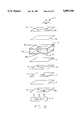
- FIG. 1 is a schematic diagram of the optical components of a normally white (NW) twisted nematic (TN) liquid crystal display (LCD) including a pair of negative tilted retarders and a pair of negative non-tilted biaxial retarders all on one side of the liquid crystal layer, according to an embodiment of this invention.
- NW normally white
- TN twisted nematic
- LCD liquid crystal display
- FIG. 2 illustrates the angular relationship between the respective axes of the optical components of the FIG. 1 embodiment, as viewed from the point of view of the viewer 1 (i.e. as viewed from the front of the display).
- FIG. 3 is a schematic diagram of the optical components of an NW twisted nematic LCD including a pair of negative tilted retarders and a pair of negative non-tilted retarders all on one side of the liquid crystal layer, according to another embodiment of this invention.
- FIG. 4 illustrates the angular relationship between the respective axes of the FIG. 3 embodiment of this invention, as viewed from the point of view of the viewer.
- FIG. 5 is a schematic diagram of the optical components of an NW twisted nematic LCD similar to that shown in FIGS. 3-4, except that the FIG. 5 display includes an additional retarder located on the side of the liquid crystal layer opposite the tilted retarders, according to an embodiment of this invention.
- FIG. 6 illustrates the angular relationship between the respective axes of the optical components of the FIG. 5 display, as viewed from the point of view of the viewer.
- FIG. 7 is a side cross-sectional view of an NW twisted nematic LCD according to any of the FIGS. 1-4 embodiments.
- FIG. 8 is a side cross-sectional view of an NW twisted nematic LCD according to the FIGS. 5-6 embodiment.
- FIG. 9 is a schematic view of the optical components of an NW TN LCD according to another embodiment of this invention wherein the two tilted retarders positioned rearwardly of the LC layer are adjacent one another with no other retarders therebetween.
- FIG. 10 is a schematic view of an NW TN LCD according to still another embodiment of this invention.
- FIG. 11 is a schematic view of a NW TN LCD according to another embodiment of this invention wherein the two non-tilted negative retarders located rearward of the LC layer are surrounded by a corresponding pair of negative tilted retarders.
- FIG. 12 is a light contrast ratio contour graph of the NW TN light valve (LV) of Example 1 herein.
- FIG. 13 is an intensity versus vertical viewing angle along the 0° horizontal viewing axis, for a plurality of driving voltages, for the light valve of Example 1 herein, this graph illustrating, from about -20° to +60° vertical virtually no gray scale inversion, good separation, each of which while maintaining high contrast shown in FIG. 12 in the viewing zone at issue.
- FIG. 14 is an intensity (fL) versus horizontal viewing angle graph along the 15° vertical viewing axis for a plurality of different driving voltages, for the light valve of Example 1 herein, this graph illustrating from -60° to +60° horizontal virtually no gray scale inversion and good separation, while maintaining high contrast as shown in FIG. 12.
- FIG. 15 is a simulated green light (550 nm) contrast ratio contour graph of the simulated NW TN LV of Example 2 herein with an off state driving voltage of 1.8 volts and an on-state driving voltage of 5.4 volts.
- FIG. 16 is a transmission versus vertical viewing angle gray scale linearity graph along the 0° horizontal viewing axis, for a plurality of driving voltages, of the simulated LV of Example 2 herein.
- the transmission axis (vertical axis) represents light incident divided by light transmitted.
- FIG. 17 is a transmission versus horizontal viewing angle gray scale linearity plot along the 0° vertical viewing axis, for a plurality of different voltages, of the simulated NW TN LV of Example 2 herein.
- FIG. 18 is a transmission versus driving voltage (volts) plot for the simulated LV of Example 2 herein, for a plurality of different horizontal viewing angles located along the 0o vertical viewing axis.
- FIG. 19 is a white light contrast ratio graph of the Example 3 NW thin film transistor (TFT) RGBW AMLCD, with an off-state driving voltage of 1.73 volts (i.e. white voltage) and an on-state driving voltage of 5.77 volts (darkened voltage).
- TFT thin film transistor
- FIG. 20 is a white light contrast ratio graph of the NW TN LV of Example 4 herein, with an off-state driving voltage of 1.8 volts and an on-state driving voltage of 5.5 volts, this LV including in addition to the negative tilted and non-tilted retarders on the rear side of the LC, a slightly biaxial retarder located on the front side of the liquid crystal layer.
- FIG. 21 is a white light contrast ratio graph of the Example 5 NW TN light valve having a cell gap "d" of 5.20 ⁇ m, an on-state driving voltage of 5.5 volts, and an off-state driving voltage of 1.7 volts.
- FIG. 22 is a white light contrast ratio graph of the Example 6 NW TN LV having a cell gap "d" of 5.2 ⁇ m, an on-state driving voltage of 5.5 volts, and an off-state driving voltage of 0 volts.
- FIG. 23 is a white light contrast ratio graph of the Example 7 NW TN LV having a 5.20 ⁇ m cell gap, an on-state driving voltage of 5.5 volts, an off-state driving voltage of 0 volts, and a 100 nm negative uniaxial retarder (C-plate) disposed on the front side of the LC layer.
- C-plate 100 nm negative uniaxial retarder
- FIG. 24 is a green light (550 nm) simulated contrast ratio graph of the Example 8 simulation of an LV.
- FIG. 1 is an exploded schematic view of the optical components, and their respective orientations, of a twisted nematic NW LCD according to a first embodiment of this invention, this LCD being either a light valve (LV) or an AMLCD having a matrix array of pixels and colored (e.g. RGB, RGBG, RGGB, or RGBW) subpixels therein according to different embodiments of this invention.
- LV light valve
- AMLCD AMLCD having a matrix array of pixels and colored (e.g. RGB, RGBG, RGGB, or RGBW) subpixels therein according to different embodiments of this invention.
- this display includes from the rear forward toward viewer 1, conventional backlight 3, rear or light-entrance linear polarizer 5, first rear tilted negative uniaxial retarder 2, first rear negative retarder 4 (which may be either uniaxial or biaxial including indices of refraction n x , n y , and n z ), second rear tilted negative uniaxial retarder 6, second rear negative retarder 7 which may be either uniaxial or biaxial, rear buffing or orientation film 9, twisted nematic (TN) liquid crystal (LC) layer 10, front buffing or orientation film 11, and finally front or light-exit linear polarizer 15 (analyzer).
- the LCD or LV is viewed by viewer 1.
- Glass substrates are located on opposite sides of liquid crystal layer 10 so as to be disposed, for example, between the respective orientation films and their adjacent polarizers.
- Driving electrodes are disposed on and between the substantially transparent substrates and their adjacent orientation layers.
- a key to our invention is the surprise finding that when the negative tilted retarders 2 and 6 and negative retarders 4 and 7 referenced above are placed on one side of the LC (e.g. the rear side) and are within a particular retardation value(s) range and/or ratio, and/or are arranged in predetermined positions in the LCD, improved viewing characteristics of the display result.
- the viewing angle of the LCD with respect to contrast ratio is wider/larger, while inversion is lessened, both in a particular viewing zone in some embodiments such as the positive vertical zone which is so important to aircraft pilots.
- Retarders 2, 4, 6, and 7 are said to be "negative” as refractive index n z in each of them is less than both indices n x and n y (i.e. negative birefringence).
- Indices of refraction n x and n y while being co-planar, are oriented at a 90° angle relative to one another in the plane(s) of the respective film(s).
- Index of refraction n z is perpendicular to the plane defined by the n x and n y directions (i.e. the n z direction is normal to the film plane(s).
- Negative non-tilted retarders 4 and 7 each have a retardation value d ⁇ (n x -n z ) of from about +10 to +150 nm (preferably from about +10 to +80 nm), and a retardation value d ⁇ (n x -n y ) of from about -20 to +20 nm, in certain embodiments where "d" is the thickness of the retarder or compensator!.
- Retarders 4 and 7 may be made, for example, of triacetyl cellulose (TAC) having a thickness of about 120 ⁇ m or of any of the other materials disclosed in U.S. Pat. No. 5,583,679, incorporated herein by reference. Each of these retarders may also include a thin gelatin layer thereon (0.1 ⁇ m) and a polyvinyl alcohol coating solution which is rubbed as discussed in the '679 patent.
- TAC triacetyl cellulose
- Negative tilted anisotropic retarders or compensators 2 and 6 (e.g. made of a compound having a discotic structure unit in its molecule such as a discotic liquid crystalline compound having low molecular weight such as monomer and a polymer obtained by polymerization of a polymeric discotic LC compound) have tilted optical axes T 1 and T 2 , respectively.
- Each retarder 2 and 6 is from about 1.5 to 3.0 ⁇ m thick according to this invention. Because each of axes T 1 and T 2 are angled relative to both the vertical and horizontal, each defines both a polar angle (i.e.
- the polar angle (i.e. tilt angle or inclined angle of the optical axis) of each of retarders 2 and 6 varies (either continuously or intermittently in either direction) throughout the thickness of the film while the azimuthal angle remains substantially constant.
- the polar angle of one or both of retarders 2 and 6 may vary continuously from about 5° to 65° with increase of distance in the direction of the depth of the layer.
- the inclined or polar angle varies within the range of from 5° to 85° (preferably from about 10° to 80°) while the minimum polar angle in the film is in the range of from about 0° to 85° (preferably from about 5° to 40°) and the maximum polar angle is from about 5° to 90° (preferably from about 30° to 85°).
- each tilted retarder is oriented on the rear side of LC layer 10 so that the minimum tilt angle is closest to the LC layer 10 and the maximum tilt angle is closest to the backlight.
- Tilted negative retarders 2 and 6 each include refractive indices n x , n y , and n z , as well as extraordinary refractive index n e for the optical axis of symmetry of the discotic molecule structure, and ordinary refractive index n o which is perpendicular to n e as known in the art.
- each of retarders 2 and 6 has an n e of from about 1.40 to 1.65, preferably from about 1.45 to 1.60, and an n o of from about 1.45 to 1.70, preferably from about 1.5 to 1.6.
- each of retarders 2 and 6 has a thickness of from about 1.5 to 3.0 ⁇ m, and a ⁇ n (i.e. n e -n o ) value of from about -0.30 to +0.20, preferably from about -0.20 to +0.10, and most preferably from about -0.10 to 0.0.
- retarders 2 and 4 may be laminated or otherwise formed together as one unit as discussed in the '679 patent, as may retarders 6 and 7.
- An orientation and a subbing layer may be provided between layers 2 and 4 (and between layers 6 and 7).
- Retarders 2, 4, 6, and 7 may be obtained from Fuji Photo Film Co., Ltd., Japan, or alternatively from Nitto Denko America, as WV-film.
- Backlight 3 is conventional in nature and emits substantially collimated, or alternatively diffused (in Examples herein), light toward the display panel.
- Backlight 3 may be, for example, the backlighting assembly disclosed in U.S. Pat. No. 5,161,041, the disclosure of which is hereby incorporated herein by reference.
- Other conventional high intensity substantially collimated or diffuse backlight assemblies may also be used.
- Rear and front polarizers, 5 and 15 respectively may be iodine based absorption and linear in nature according to certain embodiments of this invention, and their respective linear transmission axes P R and P F are oriented perpendicular to one another (i.e. about 90° from one another ⁇ about 10° (i.e. substantially perpendicular) in either direction) so that LCDs and LVs of the different embodiments of this invention are of the normally white (NW) twisted nematic (TN) type. Therefore, when a driving voltage (e.g.
- transmission axes P R and P F of polarizers 5 and 15, respectively, are oriented such that the light emitted from backlight 3 proceeds through and is linearly polarized in direction P R by rear polarizer 5, is then twisted (e.g. from about 80° to 100°, preferably about 90°) by twisted nematic LC layer 10, and finally exits front polarizer or analyzer 15 via transmission axis P F thus reaching viewer 1 with an image.
- the light reaches viewer 1 because its polarization direction upon reaching front polarizer 15 is similar to the direction defined by transmission axis P F .
- a NW display or pixel to which a voltage less than V th is applied is said to be in the "off-state” and appears white (or colored if color filters are present) to the viewer.
- These conventional polarizers 5 and 15 are commercially available from, for example, Nitto Denko America, as #G1220DUN.
- transmission axis P R and transmission axis P F are oriented in a manner substantially perpendicular to one another as discussed above.
- polarizers 5 and 15 may alternatively be oriented in other manners which also render the display of the NW type.
- Important aspects of this invention which result in the improved viewing characteristics (better contrast and less inversion) disclosed herein include (i) the substantially parallel orientation (i.e. within ⁇ 10° from parallel in either direction) of the azimuthal angle of axis T 2 of tilted retarder 6 relative to the transmission axis P R of the rear polarizer (see, for example, FIGS. 2, 4, and 6); (ii) each of the rear and front polarizers 5 and 15 having its transmission axis aligned parallel ⁇ 10° (i.e.
- each of the tilted retarders 2 and 6 being oriented so that the side having the largest or maximum tilt angle is closest to the backlight 3 and is first hit by light emitted therefrom, and the minimum tilt side is furtherest from the backlight; (iv) the substantial perpendicular orientation of axes T 1 and T 2 (with respect to azimuthal angle); (v) the substantial anti-parallel ( ⁇ about 10° from anti-parallel in either direction) orientation of the azimuthal angle of T 1 and front buffing direction B F e.g. see FIGS. 2, 4, and 6!
- Rear and front orientation or buffing films 9 and 11, respectively, are each from about 250-500 ⁇ thick, and may be made of a substantially transparent polyimide material as is known in the art.
- Rear LC orientation film 9 is conventionally buffed or oriented in direction B R as shown in FIGS. 1-11.
- front LC orientation film 11 is conventionally buffed in direction B F .
- Buffing directions B R and B F are oriented substantially perpendicular to one another so as to allow the molecules of liquid crystal layer 10, when in the off or non-driven state, to be twisted from about 80° to 100°, preferably about 90°.
- the instant invention may be used in conjunction with multi-domain e.g. two-doman! alignment applications.
- Liquid crystal layer 10 has a thickness "d" of from about 3.5 to 6.5 ⁇ m according to certain embodiments, preferably from about 4.0 to 5.0 ⁇ m.
- LC layer 10 has a birefringent value ⁇ n of from about 0.08 to 0.10 according to certain embodiments, preferably from about 0.084 to 0.086 at room temperature.
- Negatively birefringent tilted retardation plates or films, 2 and 6, with tilted and azimuthal angled optical axes T 1 and T 2 respectively (i.e. axes), in the FIGS. 1-2 embodiment are both disposed on the rear side of LC layer 10 in order to reduce ambient reflections off of the front of the display panel. Accordingly, retarders 4 and 7 are also on the rear side of LC 10.
- the n x index direction of retarder 4 differs from the n x index direction of retarder 7 by from about 80°-100°, preferably about 90°, while their respective planes are parallel e.g. see FIGS. 1-11!.
- the retarders and polarizers herein may all be separate sheets, although they alternatively may be all integrally formed or laminated together (or even deposited onto one another) with a known laminating material or deposition process according to certain embodiments.
- films 2, 4, and 5, for example may be laminated or otherwise formed together to form a single sheet having negative tilted retarder 2, negative retarder 4, and polarizer 5.
- films 6 and 7 may be formed together as one unit, although this, of course, does not affect the existence of two different retarders/films 6 and 7.
- FIG. 2 illustrates the relationship between the FIG. 1 axes, from the point of view of viewer 1.
- transmission axis P F of front polarizer 15 is substantially perpendicular to axis P R of rear polarizer 5.
- the front polarizer axis P F is aligned at the 46° (and 226°) angle while the rear polarizer axis P R is at the 135° (and 315°) angle.
- front buffing direction B F is perpendicular to rear buffing direction B R .
- front buffing direction B F is aligned at 45° while the rear buffing direction B R is at 315°.
- the azimuthal angle of retarder 2 (defining axis T 1 ) is substantially perpendicular to the azimuthal angle of retarder 6 (defining axis T 2 ).
- T 1 is aligned at 225° while T 2 is aligned at 315°. It is also important that T 1 is substantially anti-parallel to B F .
- P F and B F are substantially parallel to one another, while P R , B R , and T 2 are also parallel to one another, ⁇ approximately 10° (i.e. substantially parallel).
- FIG. 3 is an exploded schematic view of the optical components of an NW twisted nematic LCD (or LV) according to another embodiment of this invention.
- the display of FIGS. 3-4 is similar to that of FIGS. 1-2, except that in the FIGS. 3-4 embodiment, the buffing directions and azimuthal angles of the tilted retarders 2 and 6, and possibly the angles of negative retarders 4 and 7, are oriented in different directions.
- axes P F and P R of the front and rear polarizers are substantially perpendicular to one another as in the FIGS. 1-2 embodiment.
- buffing direction B F of front buffing film 11 is in the third quadrant and is substantially parallel to front polarizer axis P F and substantially anti-parallel to axis T 1 (azimuthal angle) of retarder 2.
- the rear buffing direction B R of film 9 is in the second quadrant and is substantially parallel to rear polarizer axis P R
- the azimuthal angle of its tilted axis is in the second quadrant and is substantially parallel to the axis P R of rear polarizer 5.
- P F is oriented at 45°, P R at 134°, B R at 135°, B F at 225°, T 1 at 44°, and T 2 at 134°.
- the polarizer axes extend through the origin and are present in two separate opposing quadrants, while the buffing directions and inclined angle azimuthal directions extend from the origin into only a single quadrant. It is important to note that although the buffing directions have changed in the FIGS. 3-4 embodiments, P R and T 2 are still substantially parallel, while T 1 and T 2 remain substantially perpendicular to one another and T 1 is substantially anti-parallel to B F .
- FIG. 5 is an exploded schematic view of the optical components of a NW twisted nematic LCD (or LV) according to another embodiment of this invention, wherein an additional retarder 16 is located on the front side of liquid crystal layer 10.
- Retarder 16 may either be a positive uniaxial retarder (A-plate) having a retardation value of from about 50-200 nm, a negative uniaxial retarder (C-plate) having a retardation value of from about 50-200 nm, or a slightly biaxial negative retarder wherein n x >n y >n z .
- retarder 16 is a negative biaxial retarder having a retardation value d ⁇ (n x -n z ) of from about 0 to 100 nm (preferably about 10-50 nm, and most preferably about 30 nm), with the slight biaxial nature of retarder 16 including an axis n x directed in angular direction R as shown in FIG. 6 which is substantially parallel ⁇ about 10° to axis P F .
- the FIGS. 5-6 embodiment is similar to that of FIGS. 3-4.
- Angle 21 defining the position of axis P F may be at from about 35° to 55°, and preferably approximately 45°; the angle 20 may be from about 0°-10°, in either direction relative to P F , and preferably from about 0°-5° in either direction; angle 22 may be from about 35°-55°, preferably 45°; angle 23 may be from about 0°-10° in either direction relative to P R , preferably from about 0°-5° in either direction; angle 24 may be from about 35°-55°, preferably approximately 45°; angle 25 may be from about 35°-55°, preferably approximately 45°; angle 26 may be from about 0°-10° in either direction relative to T 1 , and preferably from about 0°-5° in either direction; angle 27 may be from about 35°-55°, and preferably approximately 45°; and angle 28 may be from about 35°-55°, and preferably approximately 450°.
- FIG. 7 is a side cross-sectional view of an NW twisted nematic LCD or LV of any of FIGS. 1-4, according to certain embodiments of this invention.
- the display includes rear polarizer 5, adhesive layer 31, first negative tilted retarder 2, first negative retarder 4 (either uniaxial or biaxial), adhesive layer 32, second negative tilted retarder 6, second negative retarder 7 (either uniaxial or biaxial), substantially transparent glass or plastic substrate 33, conductive electrode(s) 34, rear buffing or orientation film 9, twisted nematic liquid crystal (LC) layer 10, front orientation or buffing film 11, front conductive electrode(s) 35 which functions in conjunction with rear electrode(s) 34 in order to apply voltage across LC layer 10 and/or individual pixels or subpixels defined therein, front substantially transparent glass or plastic substrate 36, and finally front polarizer 15.
- LC liquid crystal
- front conductive electrode(s) 35 which functions in conjunction with rear electrode(s) 34 in order to apply voltage across LC layer 10 and/or individual pixels or subpixels defined
- adhesive layers 31 and 32 abut the tilted retarder layers 2 and 6, respectively, and the polar or inclined angles of retarders 2 and 6 decrease (continuously or intermittently) as a function of the depth or thickness of the retarders as a function of distance from their adjacent adhesive layers 31 and 32, respectively.
- the incline or polar angle of the optical axis T 1 of retarder 2 may continuously vary, for example, from a maximum of 65° in the area of film 2 adjacent adhesive 31, to 5° adjacent retarder layer 4.
- the plane of the discotic structure in negative tilted retarder 2 has a planar incline angle that is continuously reduced from a tilt of 65° to one of 5° from the rear edge of layer 2 (i.e.
- Layer 6 has its polar or incline angle vary (continuously or intermittently) in a similar manner, so that the incline from the normal decreases as a function of distance from adhesive layer 32.
- Exemplary variations of polar angles for each of retarders 2 and 6 are: (i) from 65° to 5° going away from the adhesive layer that is disposed adjacent the tilted retarder toward LC layer 10; (ii) from 50° to 20° going away from the adhesive layer that is disposed adjacent the tilted retarder; (iii) from 70° to 20° going away from the adhesive layer adjacent the tilted retarder; and (iv) from 40° to 20° going away from the adhesive layer adjacent the tilted retarder.
- the azimuthal angles of axes T 1 and T 2 remain substantially constant while the incline angles vary either continuously or intermittently as discussed above.
- FIG. 7 shows each tilted retarder (e.g. 2) being disposed between LC layer 10 and its adjacent adhesive layer (e.g. 31), this need not be the case.
- layers 2, 4, and 31 may be flipped over so that the adhesive 31 is between the retarder 2 and the LC 10 so that the tilt angle of layer 2 increases from, e.g. 5° to 65°, throughout layer 2 going toward LC layer 10 away from adhesive 31.
- FIG. 8 is a side cross-sectional view of the TN NW LCD or LV of FIGS. 5-6. This particular display is similar in structure to that of FIG. 7 discussed above, except that additional retarder layer 16 (discussed above) is located on the front side of LC layer 10 in between front optically transparent substrate 36 and front polarizer 15.
- the retardation value d ⁇ (n e -n o ) of each of the two tilted negative retarders 2 and 6 is from about -20 to -200 nm, preferably about -50 nm to -150 nm, and most preferably from about -100 nm to -150 nm, and where n e ⁇ n o .
- the d ⁇ (n x -n z ) birefringent value (retardation value) of each of negative retardation films 4 and 7 is from about 10 to 150 nm, more preferably from about 10 to 80 nm.
- the absolute value ratio of the average retardation values d ⁇ (n e -n o ) of each or one of negative tilted retarders 2 and 6 to the retardation value d ⁇ (n x -n z ) of each or one of retarders 4 and 7 is from about 1:1 to 3:1 (more preferably from about 1.0:1 to 2.0:1) according to certain embodiments.
- the retardation values of each of the like (e.g. tilted) retarders need not be identical, but the ratio range is typically met by both sets of retardation values.
- FIG. 9 is an exploded schematic view of an NW TN LCD or LV according to another embodiment of this invention, including optional retarder(s) 16.
- the pair of negative tilted retarders 2 and 6 located rearwardly of LC layer 10 are sandwiched between negative retarders 4 and 7.
- this embodiment includes rear polarizer 5, first negative retarder 4, first tilted retarder 2, second tilted retarder 6, and second negative retarder 7.
- the orientation of the optical axes of the different components of the FIG. 9 embodiment are illustrated, for example, in either of FIGS. 4 and 6 discussed above.
- FIG. 10 is an exploded schematic view of an NW TN LCD or LV according to another embodiment of this invention, including optional retarder(s) 16.
- the FIG. 10 embodiment differs from those illustrated and discussed above in that tilted retarder 6 is the retarder most closely located relative to rear orientation layer 9 and retarder 4 is positioned closest to rear polarizer 5.
- tilted retarder 6 is the retarder most closely located relative to rear orientation layer 9 and retarder 4 is positioned closest to rear polarizer 5.
- rear linear polarizer 5 we have from the rear forward to the viewer 1, rear linear polarizer 5, negative retarder 4, first tilted retarder 2, negative retarder 7, and second tilted retarder 6.
- the orientation of the optical axes of the various components of this embodiment are shown, for example, in either of FIGS. 4 and 6 as discussed above.
- FIG. 11 is an exploded schematic view of an NW TN LCD or LV according to still another embodiment of this invention, including optional retarder(s) 16.
- the two negative retarders 4 and 7 are both disposed between negative tilted retarders 2 and 6 on one side (e.g. rear) of the liquid crystal cell.
- the optical orientation of the components of this embodiment may be illustrated, for example, in either of FIGS. 4 and 6 as discussed above.
- the optical axes of this embodiment may be aligned as shown in FIG. 2 above.
- one of retarders 4 and 7 may be removed.
- each of the embodiments illustrated and discussed above includes retarders 2, 4, 6, and 7, all located on the rear side of liquid crystal layer 10. This is to avoid undesirable ambient light reflections off of the front of the display during certain applications.
- retarders 2, 4, 6, and 7 may optionally be located on the front side of the liquid crystal layer 10, in which case, each of the retarders would be rotated symmetrically.
- the retarders 2, 4, 6, and 7 of FIG. 3 were all to be positioned on the front side of liquid crystal layer 10, then they would be rotated symmetrically so that axis T 1 of retarder 2 (located closest to the front polarizer) would be substantially anti-parallel to the buffing direction B R of rear orientation film 9, and so on.
- the liquid crystal layer had a ⁇ n (or birefringent value) of 0.0854
- the thickness "d" of LC layer 10 in each LV or LCD was substantially constant across the entire viewing area
- the front and rear linear polarizers 5 and 15 were linear and each included both an iodined PVA layer and a TAC layer on each side of the PVA as known in the art
- the retarders 2, 4, 6, and 7 were all present and located on the rear side of liquid crystal layer 10 so as to be disposed between the liquid crystal cell and backlight 3.
- All polarizers were NPF-G1220DUN.
- retarders 2 and 4 along with adhesive 31 were a single unit, with layer 4 including an orienting triacetyl (triacetate) cellulose (TAC) layer and an orienting layer, and layer 2 including a discotic liquid crystalline compound formed on the TAC layer, with the tilt or polar angle varying continuously downward (i.e. decreasing) going away from adhesive 31.
- Layers 6, 7, and 32 were similarly formed as one unit and had the same characteristics.
- the tilted retarders were always located between the corresponding non-tilted TAC retarder and the corresponding adhesive.
- the azimuthal aspect of T 1 was always substantially anti-parallel to B F
- T 2 was always substantially parallel to B R .
- a normally white (NW) light valve (LV) was constructed as shown in FIGS. 1, 2, 7, and 12-14.
- This light valve had, from the rear forward, rear polarizer 5 having a PVA layer and a pair of TAC layers NPF-G1220DUN! first tilted retarder 2, first non-tilted negative retarder 4, second tilted retarder 6, second non-tilted retarder 7, rear orientation film 9, LC layer 10, front orientation film 11, and finally front polarizer 15 NPF-G1220DUN!.
- the thickness "d" of LC layer 10 was 5.2 ⁇ m and the An value of LC layer 10 was 0.0854.
- each of retarders 2 and 7 varied throughout the thickness of the layers from 60°-70° on the side closest to backlight 3 down to approximately 5° on the side closest to liquid crystal layer 10.
- the tilt or incline angle of retarder 2 was from about 60°-70° on the side of this layer adjacent polarizer 5 and it continuously varied down to approximately 5° on the side of the layer proximate retarder 4.
- FIG. 12 is a white light contrast ratio graph of the LV of this first Example, when 5.0 volts were applied in the on-state and 1.8 volts in the off-state. As illustrated, this LV exhibited very fine contrast throughout the entire viewing zone, especially in the positive vertical viewing areas. This LV exhibited contrast of at least about 30:1 over a horizontal angular span of at least about 120°, including at vertical viewing angles of 0°-10°.
- FIG. 13 is an intensity (fL) versus vertical viewing angle plot, at a plurality of different gray level driving voltages, for the LV of this first Example along the 0° horizontal viewing axis. As shown, there is virtually no gray scale inversion from -20° vertical all the way up to +60° vertical, and there is provided excellent separation of the gray scale voltages in this particular viewing zone.
- FIG. 14 is an intensity (fL) versus horizontal viewing angle plot, at a plurality of different gray level driving voltages, for the LV of this first Example along the 15° vertical viewing axis. As illustrated, from the horizontal viewing angle of -60° to +60°, there was excellent separation, no crossovers (i.e. excellent gray scale inversion characteristics).
- an NW TN LV was simulated based upon algorithms which may be found in SID 1991, pages 586-589, entitled "Application Of The Extended Jones Matrix Method To LCDs At The Oblique Incidence", by A. Lien.
- This simulated NW TN LV is fairly represented by FIGS. 1, 2, and 15-18 herein. From the rear forward, this LV included rear polarizer 5, negative tilted retarder 2, negative uniaxial retarder 4, negative tilted retarder 6, negative uniaxial retarder 7, rear orientation film 9, liquid crystal layer 10, front orientation film 11, and front polarizer 15.
- the thickness of LC layer 10 was 5.2 ⁇ m, and the ⁇ n of the LC layer was 0.0854.
- FIG. 15 is a green light contrast ratio of the LV of this Example when 5.4 volts were applied in the on-state and 1.8 volts in the off-state.
- excellent contrast resulted with the LV exhibiting contrast of at least 100:1 over a horizontal viewing range or extent of 110°, all the way from -60° to +50° between 10° and 20° vertical.
- the LV of this Example exhibited contrast of at least 90:1 over a horizontal span of at least 120°, and a contrast of at least 30:1 over a vertical span of at least about 105°.
- FIG. 16 is a transmission versus vertical viewing angle plot, along the 0° horizontal viewing axis, for a plurality of different voltages, for this LV.
- FIG. 16 shows that there was virtually no gray scale inversion from -5° vertical all the way up to +60 ° vertical.
- good gray scale separation was exhibited in this range.
- the display exhibited both excellent gray scale behavior and superior contrast (FIG. 15) in the same viewing zone (e.g. the upper vertical). This is an improvement over the prior art.
- FIG. 17 is a transmission versus viewing angle plot of the LV of this Example, for a plurality of different driving voltages, at a plurality of different horizontal angles at the 0° vertical viewing axis. Again, excellent separation and inversion characteristics are illustrated.
- FIG. 18 is a transmission versus voltage plot for a plurality of horizontal viewing angles along the 0 ° vertical viewing axis. As shown, this display exhibited excellent gray scale behavior with regard to both separation and inversion.
- an NW TN RGBW AMLCD was manufactured and tested as shown substantially in FIGS. 1, 2, 7, and 19.
- the AMLCD of this third Example included an average cell gap "d" of about 4.9 ⁇ m. From the rear forward, this AMLCD included rear polarizer 5 (PVA and TAC), tilted retarder 2, slightly biaxial negative retarder 4, tilted retarder 6, slightly biaxial negative retarder 7, rear orientation film 9, LC layer 10, front orientation film 11, and finally front polarizer 15.
- the color filters, driving electrodes, glass substrates, and driving TFTs were also included as this was a full AMLCD.
- Retarders 2 and 4 along with adhesive 31 were obtained as a single unit from Fuji, as were retarders 6 and 7 and adhesive 32, as its WV film.
- the optical axes of the various components of this Example were oriented as follows: P F at 46°, P R at 135°, B F at 45°, B R at 315°, T 1 at 225°, and T 2 at 315°.
- the retardation value (n x -n z ) ⁇ d for each of retarders 4 and 7 was approximately 40 nm, while the retardation value
- the tilt or incline angle for each of retarders 2 and 6 varied from in the range of 60°-70° nearest the backlight down to around 5° on the side closest to the liquid crystal layer. As in all embodiments herein, the azimuthal angle remain constant in each of retarders 2 and 6 while the tilt angle varied throughout the thickness of the layers.
- FIG. 19 is a white light contrast ratio graph of the AMLCD of this third Example when 5.77 volts were applied in the on-state and 1.73 volts in the off-state. As can be seen, this AMLCD exhibited excellent contrast ratios throughout the viewing zone. The maximum measured contrast ratio, at the "+”, was 373.48, while the minimum was 2.89.
- an NW TN LV was manufactured and tested as follows.
- This LV is generally illustrated in FIGS. 5, 6, 8, and 20 herein.
- the LC layer 10 of this LV had a thickness of 5.20 ⁇ m.
- This LV included from the rear forward, rear polarizer 5, tilted retarder 2, slightly biaxial negative retarder 4, tilted retarder 6, slightly biaxial negative retarder 7, rear orientation film 9, LC layer 10, front orientation film 11, slightly biaxial negative retarder 16 obtained from Kodak, and finally front polarizer 15.
- the retardation value of retarder 16 (which was almost, but not quite, a negative uniaxial retarder) was -30 nm.
- Retarders 2, 4, 6, and 7 were obtained from Fuji and configured as discussed in Example 3 above.
- Retarder 16 had a retardation d ⁇ (n x -n z ) of about 30 nm.
- FIG. 20 is a white light contrast ratio graph of the LV of this fourth Example, when 5.5 driving volts were applied in the on- (or darkened) state and 1.5 volts in the off- (or whitened) state.
- the maximum contrast was 341.53 while the minimum was 0.48.
- FIG. 20 should be interpreted by adding 180° to each of the angles defined in this Example, because it was taken upside down. This is also the case for FIGS. 21-23.
- an NW TN LV was manufactured and tested as follows. This LV is best illustrated by FIGS. 11 and 21 herein. From the rear forward, this LV included rear polarizer 5, adhesive 31, retarder 2, retarder 4, retarder 7, retarder 6, adhesive 32, buffing film 9, LC layer 10, front buffing film 11, and front polarizer 15.
- Retarders 2-6 were obtained from Fuji as discussed above in Example 3 and were configured as described.
- FIG. 21 is a white light contrast ratio plot of the LV of this fifth Example, when 5.5 volts were applied in the on-state and 1.7 volts in the off-state.
- the LC layer of this fifth Example had a thickness of 5.20 ⁇ m.
- the maximum contrast ratio of this LV was 199.38, while the minimum was 0.52.
- an NW TN LV having a LC thickness of 5.2 ⁇ m was made and tested as follows. This LV is best illustrated by FIGS. 3, 4, 7, and 22 herein. From the rear forward, the LC included the components illustrated in FIG. 3. They were oriented as follows: P F at 46°, P R at 135°, B R at 135°, B F at 225°, T 1 at 45°, and T 2 at 135°. The retarders were as described in Example 3.
- FIG. 22 is a white light contrast ratio plot of the NW LV of this sixth Example, when 5.5 volts were applied in the on-state and 0 volts in the off-state.
- the maximum contrast ratio of this figure is 596.67 (at the cross) and the minimum contrast ratio was 4.16.
- FIG. 23 is a white light contrast ratio graph for the NW LV of this seventh Example, including the C-plate, when 5.5 volts were applied in the on-state and 0 volts in the off-state.
- the maximum contrast ratio of this LV in this particular plot was 264.28, while the minimum was 2.05.
- an NW TN LV was simulated based upon the algorithms described in Example 2.
- This simulated LV is fairly represented by FIGS. 1, 7, and 24 herein. From the rear forward, this LV included rear polarizer 5, negative tilted retarder 2, negative uniaxial retarder 4, negative tilted retarder 6, negative uniaxial retarder 7, rear orientation film 9 with buffing direction B R , LC layer 10, front orientation film 11 with buffing direction B F , and finally front polarizer 15.
- the thickness of LC layer 10 is 5.20 ⁇ m, while the birefringent value ⁇ n of LC layer 10 was 0.084.
- Each of negative uniaxial retarders 4 and 7 were 1.0 ⁇ m thick, had no tilt, had an n e value of 1.52, and an n o value of 1.57.
- ⁇ n (n e -n o ) for each of retarders 4 and 7 was -0.05, while d ⁇ n was -50 nm for each of retarders 4 and 7.
- each of tilted retarders 2 and 6 had a tilt which varied from 64° down to 4° throughout the thickness of the layers going toward LC layer 10.
- each of tilted retarders 2 and 6 had an n e value of 1.52 and an n o value of 1.57, and thus a ⁇ n value of -0.05.
- FIG. 24 is a green light contrast ratio graph of the LV of this eighth Example when 1.0 volts were applied in the off-state and 5.4 volts in the on-state.
- this LV exhibited excellent contrast, including a contrast ratio of at least 30:1 over a vertical angular span of at least about 100° and even up to about 110° at the -10° horizontal viewing angle. Furthermore, the LV of this Example exhibited contrast of at least about 30:1 over a horizontal angular span of at least about 80°, and even up to about 90° at the -20° and +20° vertical viewing angles.
Abstract
Description
Claims (17)
Priority Applications (5)
| Application Number | Priority Date | Filing Date | Title |
|---|---|---|---|
| US08/876,043 US5895106A (en) | 1997-06-13 | 1997-06-13 | NW twisted nematic LCD with negative tilted retarders on one side of liquid crystal cell |
| US09/066,827 US6567143B1 (en) | 1997-06-05 | 1998-04-28 | NW twisted nematic LCD with negative and tilted retarders on each side of liquid crystal cell to improve vertical contrast ratios |
| CA 2239533 CA2239533C (en) | 1997-06-05 | 1998-06-01 | Nw twisted nematic lcd with negative and tilted retarders on one side of liquid crystal cell |
| US09/088,704 US5990997A (en) | 1997-06-05 | 1998-06-02 | NW twisted nematic LCD with negative tilted retarders for improved viewing characteristics |
| EP98110258.5A EP0887691B1 (en) | 1997-06-05 | 1998-06-05 | NW Twisted nematic LCD with negative and tilted retarders on one side of liquid crystal cell |
Applications Claiming Priority (1)
| Application Number | Priority Date | Filing Date | Title |
|---|---|---|---|
| US08/876,043 US5895106A (en) | 1997-06-13 | 1997-06-13 | NW twisted nematic LCD with negative tilted retarders on one side of liquid crystal cell |
Related Child Applications (2)
| Application Number | Title | Priority Date | Filing Date |
|---|---|---|---|
| US86997397A Continuation-In-Part | 1997-06-05 | 1997-06-05 | |
| US09/088,704 Continuation-In-Part US5990997A (en) | 1997-06-05 | 1998-06-02 | NW twisted nematic LCD with negative tilted retarders for improved viewing characteristics |
Publications (1)
| Publication Number | Publication Date |
|---|---|
| US5895106A true US5895106A (en) | 1999-04-20 |
Family
ID=25366876
Family Applications (1)
| Application Number | Title | Priority Date | Filing Date |
|---|---|---|---|
| US08/876,043 Expired - Lifetime US5895106A (en) | 1997-06-05 | 1997-06-13 | NW twisted nematic LCD with negative tilted retarders on one side of liquid crystal cell |
Country Status (1)
| Country | Link |
|---|---|
| US (1) | US5895106A (en) |
Cited By (42)
| Publication number | Priority date | Publication date | Assignee | Title |
|---|---|---|---|---|
| EP1069461A2 (en) * | 1999-06-30 | 2001-01-17 | Casio Computer Co., Ltd. | Liquid crystal display with wide viewing angle range |
| US6181400B1 (en) * | 1999-11-19 | 2001-01-30 | International Business Machines Corporation | Discotic-type twist-film compensated single-domain or two-domain twisted nematic liquid crystal displays |
| US6184957B1 (en) * | 1996-05-15 | 2001-02-06 | Fuji Photo Film Co., Ltd. | Liquid crystal display having optical compensatory sheet with negative uniaxial property and an optical axis parallel to the plane of the sheet |
| US6226061B1 (en) * | 1997-03-25 | 2001-05-01 | Sharp Kabushiki Kaisha | Liquid crystal display device having phase different plates |
| US6266114B1 (en) | 1999-07-14 | 2001-07-24 | Rockwell Collins, Inc. | Method and apparatus for compensating a liquid crystal display |
| US6292244B1 (en) | 1998-01-20 | 2001-09-18 | Industrial Technology Research Institute | Manufacturing method of forming two-domain liquid crystal display by exposing a part of the orientation layer twice |
| US6356325B1 (en) * | 1997-02-05 | 2002-03-12 | Sharp Kabushiki Kaisha | LCD with compensators in the inclined direction |
| US6359671B1 (en) | 2000-02-23 | 2002-03-19 | Planar Systems, Inc. | High contrast liquid crystal device |
| US6396553B1 (en) * | 1998-06-16 | 2002-05-28 | Nec Corporation | Twisted nematic liquid crystal display device with improved viewing angle characteristics |
| US20030002154A1 (en) * | 2001-07-02 | 2003-01-02 | Giorgio Trapani | Polarizers coated with optically functional layers |
| US20030067572A1 (en) * | 2000-04-03 | 2003-04-10 | Konica Corporation | Optical compensation sheet and liquid crystal display |
| US6567143B1 (en) * | 1997-06-05 | 2003-05-20 | Guardian Industries Corp. | NW twisted nematic LCD with negative and tilted retarders on each side of liquid crystal cell to improve vertical contrast ratios |
| EP1087254A3 (en) * | 1999-08-06 | 2003-06-18 | Sharp Kabushiki Kaisha | Liquid crystal display apparatus |
| US6587171B1 (en) * | 1998-07-28 | 2003-07-01 | Thomson-Csf Sextant | Angle of view of a LCD screen by a novel birefringent film stacking |
| US6606143B1 (en) * | 1998-03-13 | 2003-08-12 | Sharp Kabushiki Kaisha | Liquid crystal display device with phase element |
| US20030193635A1 (en) * | 2002-04-12 | 2003-10-16 | Eastman Kodak Company | Optical devices comprising high performance polarizer package |
| US20030193636A1 (en) * | 2002-04-16 | 2003-10-16 | Allen Richard C. | Compensators for liquid crystal displays and the use and manufacture of the compensators |
| US6680766B1 (en) * | 1998-12-31 | 2004-01-20 | Honeywell Inc. | Liquid crystal display wherein twist angle of liquid crystal material differ from 90° by approximately 15° or more |
| US6693689B1 (en) * | 1999-03-31 | 2004-02-17 | Lg Philips Lcd Co., Ltd. | Reflective liquid crystal display device |
| EP1431782A1 (en) * | 2002-12-16 | 2004-06-23 | Nitto Denko Corporation | Optical film, elliptically polarizing plate and image display |
| US6757040B1 (en) * | 1999-05-07 | 2004-06-29 | Lg. Philips Lcd Co., Ltd. | Multi-domain liquid crystal display |
| US6770334B2 (en) * | 2000-03-29 | 2004-08-03 | Fuji Photo Film Co., Ltd. | Optically anisotropic sheet comprising aligned discotic liquid crystal molecules |
| US20040156002A1 (en) * | 2000-05-31 | 2004-08-12 | Sony Corporation | Apparatus and method for displaying image |
| WO2004088405A1 (en) * | 2003-03-28 | 2004-10-14 | Fuji Photo Film Co. Ltd. | Liquid crystal display device |
| US6806931B1 (en) * | 1998-11-20 | 2004-10-19 | Koninklijke Philips Electronics N.V. | Image projection system with improved contrast having single birefringence-compensating element |
| US6867834B1 (en) * | 1999-09-16 | 2005-03-15 | Merck Patent Gmbh | Optical compensator for LCD including stacked films of only one O-plate, one A-plate and two negative C-plate retarders |
| US20050117099A1 (en) * | 2002-02-19 | 2005-06-02 | Takashi Yamaoka | Inclined optical compensation film method for producing the same and liquid crystal display including the same |
| US6995823B1 (en) * | 2002-07-30 | 2006-02-07 | Rockwell Collins, Inc. | Viewing angle for liquid crystal display system and method |
| US20060187394A1 (en) * | 2005-02-24 | 2006-08-24 | Au Optronics Corp. | Wide viewing angle liquid crystal display panel |
| US20060268207A1 (en) * | 2005-05-25 | 2006-11-30 | Jds Uniphase Corporation | Tilted C-Plate Retarder Compensator And Display Systems Incorporating The Same |
| US20060285051A1 (en) * | 2005-06-14 | 2006-12-21 | Lg Chem, Ltd. | IPS mode liquid crystal display using two sheets of biaxial negative retardation films and a +C-plate |
| US20070064163A1 (en) * | 2005-09-09 | 2007-03-22 | Jds Uniphase Corporation | Optimally Clocked Trim Retarders |
| US20070081356A1 (en) * | 2005-10-06 | 2007-04-12 | Au Optronics Corp. | Backlight module and liquid crystal display device incorporating the same |
| US20070085972A1 (en) * | 2005-10-18 | 2007-04-19 | Jds Uniphase Corporation | Electronically Compensated LCD Assembly |
| US20070126961A1 (en) * | 2005-12-05 | 2007-06-07 | Toppoly Optoelectronics Corp. | Liquid crystal displays |
| US20070296892A1 (en) * | 2002-09-06 | 2007-12-27 | Dai Nippon Printing Co., Ltd. | Laminated retardation optical element, process of producing the same, and liquid crystal display |
| CN100371743C (en) * | 2002-10-28 | 2008-02-27 | 日东电工株式会社 | Compensation films for LCDs |
| US20080239490A1 (en) * | 2005-06-27 | 2008-10-02 | Research Foundation Of The University Of Central Florida, Incorporated | Wide-acceptance-angle circular polarizers |
| US20080252800A1 (en) * | 2007-04-10 | 2008-10-16 | Jds Uniphase Corporation | Twisted Nematic xLCD Contrast Compensation With Tilted-Plate Retarders |
| US20100245742A1 (en) * | 2009-03-25 | 2010-09-30 | Seiko Epson Corporation | Image display apparatus and viewing angle compensation method |
| JP2018189825A (en) * | 2017-05-08 | 2018-11-29 | 富士フイルム株式会社 | Laminate and display |
| WO2020116174A1 (en) * | 2018-12-04 | 2020-06-11 | 富士フイルム株式会社 | Optical laminate and polarizing plate |
Citations (6)
| Publication number | Priority date | Publication date | Assignee | Title |
|---|---|---|---|---|
| US5227903A (en) * | 1991-09-20 | 1993-07-13 | Casio Computer Co., Ltd. | Liquid crystal display device with at least one biaxial retardation film having nx >nz >ny |
| EP0679921A1 (en) * | 1994-04-29 | 1995-11-02 | OIS Optical Imaging Systems, Inc. | LCD with a pair of retardation films on one side of liquid crystal layer |
| US5570214A (en) * | 1993-12-15 | 1996-10-29 | Ois Optical Imaging Systems, Inc. | Normally white twisted nematic LCD with retardation films on opposite sides of liquid crystal material for improved viewing zone |
| US5583679A (en) * | 1994-05-31 | 1996-12-10 | Fuji Photo Film Co., Ltd. | Liquid crystal display with optical compensatory sheet having discotic molecules varyingly inclined |
| EP0774682A2 (en) * | 1995-11-15 | 1997-05-21 | OIS Optical Imaging Systems, Inc. | Normally white twisted nematic LCD with positive and negative phase retarders |
| US5638200A (en) * | 1995-02-03 | 1997-06-10 | Ois Optical Imaging Systems, Inc. | Liquid crystal display with tilted retardation film |
-
1997
- 1997-06-13 US US08/876,043 patent/US5895106A/en not_active Expired - Lifetime
Patent Citations (8)
| Publication number | Priority date | Publication date | Assignee | Title |
|---|---|---|---|---|
| US5227903A (en) * | 1991-09-20 | 1993-07-13 | Casio Computer Co., Ltd. | Liquid crystal display device with at least one biaxial retardation film having nx >nz >ny |
| US5570214A (en) * | 1993-12-15 | 1996-10-29 | Ois Optical Imaging Systems, Inc. | Normally white twisted nematic LCD with retardation films on opposite sides of liquid crystal material for improved viewing zone |
| US5594568A (en) * | 1993-12-15 | 1997-01-14 | Ois Optical Imaging Systems, Inc. | LCD with a pair of retardation films on one side of normally white liquid crystal layer |
| EP0679921A1 (en) * | 1994-04-29 | 1995-11-02 | OIS Optical Imaging Systems, Inc. | LCD with a pair of retardation films on one side of liquid crystal layer |
| US5583679A (en) * | 1994-05-31 | 1996-12-10 | Fuji Photo Film Co., Ltd. | Liquid crystal display with optical compensatory sheet having discotic molecules varyingly inclined |
| US5638200A (en) * | 1995-02-03 | 1997-06-10 | Ois Optical Imaging Systems, Inc. | Liquid crystal display with tilted retardation film |
| US5777709A (en) * | 1995-02-03 | 1998-07-07 | Ois Optical Imaging Systems, Inc. | Liquid crystal display with two positive tilted retardation films and two negative retardant films |
| EP0774682A2 (en) * | 1995-11-15 | 1997-05-21 | OIS Optical Imaging Systems, Inc. | Normally white twisted nematic LCD with positive and negative phase retarders |
Non-Patent Citations (3)
| Title |
|---|
| Patent Abstracts of Japan, 07253573, Mar. 10, 1995. * |
| WO96/15473, Pub. Date May 23, 1996 PCT. * |
| WO96/15473, Pub. Date May 23, 1996 -PCT. |
Cited By (84)
| Publication number | Priority date | Publication date | Assignee | Title |
|---|---|---|---|---|
| US6184957B1 (en) * | 1996-05-15 | 2001-02-06 | Fuji Photo Film Co., Ltd. | Liquid crystal display having optical compensatory sheet with negative uniaxial property and an optical axis parallel to the plane of the sheet |
| US6356325B1 (en) * | 1997-02-05 | 2002-03-12 | Sharp Kabushiki Kaisha | LCD with compensators in the inclined direction |
| US6226061B1 (en) * | 1997-03-25 | 2001-05-01 | Sharp Kabushiki Kaisha | Liquid crystal display device having phase different plates |
| US6567143B1 (en) * | 1997-06-05 | 2003-05-20 | Guardian Industries Corp. | NW twisted nematic LCD with negative and tilted retarders on each side of liquid crystal cell to improve vertical contrast ratios |
| US6377326B2 (en) | 1998-01-20 | 2002-04-23 | Industrial Technology Research Institute | Manufacturing method of forming two-domain liquid crystal display by exposing a part of orientation layer twice |
| US6292244B1 (en) | 1998-01-20 | 2001-09-18 | Industrial Technology Research Institute | Manufacturing method of forming two-domain liquid crystal display by exposing a part of the orientation layer twice |
| US6300993B1 (en) * | 1998-01-20 | 2001-10-09 | Industrial Technology Research Institute | Wide viewing angle liquid crystal display panel |
| US20040008309A1 (en) * | 1998-03-13 | 2004-01-15 | Sharp Kabushiki Kaisha | Liquid crystal display device with improved field angles |
| US20040008308A1 (en) * | 1998-03-13 | 2004-01-15 | Sharp Kabushiki Kaisha | Liquid crystal display device with improved field angles |
| US7009678B2 (en) | 1998-03-13 | 2006-03-07 | Sharp Kabushiki Kaisha | Liquid crystal display device with improved field angles |
| US6606143B1 (en) * | 1998-03-13 | 2003-08-12 | Sharp Kabushiki Kaisha | Liquid crystal display device with phase element |
| US7193669B2 (en) | 1998-03-13 | 2007-03-20 | Sharp Kabushiki Kaisha | Liquid crystal display device with improved field angles |
| US6396553B1 (en) * | 1998-06-16 | 2002-05-28 | Nec Corporation | Twisted nematic liquid crystal display device with improved viewing angle characteristics |
| US6587171B1 (en) * | 1998-07-28 | 2003-07-01 | Thomson-Csf Sextant | Angle of view of a LCD screen by a novel birefringent film stacking |
| US6806931B1 (en) * | 1998-11-20 | 2004-10-19 | Koninklijke Philips Electronics N.V. | Image projection system with improved contrast having single birefringence-compensating element |
| US6680766B1 (en) * | 1998-12-31 | 2004-01-20 | Honeywell Inc. | Liquid crystal display wherein twist angle of liquid crystal material differ from 90° by approximately 15° or more |
| US7310125B2 (en) * | 1999-03-31 | 2007-12-18 | Lg.Philips Co., Ltd. | Reflective liquid crystal display |
| US20040145690A1 (en) * | 1999-03-31 | 2004-07-29 | Kim Yong Beom | Reflective liquid crystal display device |
| US6693689B1 (en) * | 1999-03-31 | 2004-02-17 | Lg Philips Lcd Co., Ltd. | Reflective liquid crystal display device |
| US6757040B1 (en) * | 1999-05-07 | 2004-06-29 | Lg. Philips Lcd Co., Ltd. | Multi-domain liquid crystal display |
| EP1069461A3 (en) * | 1999-06-30 | 2003-01-22 | Casio Computer Co., Ltd. | Liquid crystal display with wide viewing angle range |
| EP1069461A2 (en) * | 1999-06-30 | 2001-01-17 | Casio Computer Co., Ltd. | Liquid crystal display with wide viewing angle range |
| US6307608B1 (en) * | 1999-06-30 | 2001-10-23 | Casio Computer Co., Ltd. | Liquid crystal display having wide viewing angle range |
| US6266114B1 (en) | 1999-07-14 | 2001-07-24 | Rockwell Collins, Inc. | Method and apparatus for compensating a liquid crystal display |
| EP1087254A3 (en) * | 1999-08-06 | 2003-06-18 | Sharp Kabushiki Kaisha | Liquid crystal display apparatus |
| US6867834B1 (en) * | 1999-09-16 | 2005-03-15 | Merck Patent Gmbh | Optical compensator for LCD including stacked films of only one O-plate, one A-plate and two negative C-plate retarders |
| US6181400B1 (en) * | 1999-11-19 | 2001-01-30 | International Business Machines Corporation | Discotic-type twist-film compensated single-domain or two-domain twisted nematic liquid crystal displays |
| US6359671B1 (en) | 2000-02-23 | 2002-03-19 | Planar Systems, Inc. | High contrast liquid crystal device |
| US7052745B2 (en) * | 2000-03-29 | 2006-05-30 | Fuji Photo Film Co., Ltd. | Optically anisotropic sheet comprising aligned discotic liquid crystal molecules |
| US6770334B2 (en) * | 2000-03-29 | 2004-08-03 | Fuji Photo Film Co., Ltd. | Optically anisotropic sheet comprising aligned discotic liquid crystal molecules |
| US20040245499A1 (en) * | 2000-03-29 | 2004-12-09 | Fuji Photo Film Co., Ltd. | Optically anisotropic sheet comprising aligned discotic liquid crystal molecules |
| US20030067572A1 (en) * | 2000-04-03 | 2003-04-10 | Konica Corporation | Optical compensation sheet and liquid crystal display |
| US7218367B2 (en) * | 2000-04-03 | 2007-05-15 | Konica Corporation | Optical compensation sheet and liquid crystal display |
| US20040156002A1 (en) * | 2000-05-31 | 2004-08-12 | Sony Corporation | Apparatus and method for displaying image |
| US6885422B2 (en) * | 2000-05-31 | 2005-04-26 | Sony Corporation | Apparatus and method for displaying image |
| US20070013818A1 (en) * | 2001-07-02 | 2007-01-18 | 3M Innovative Properties Company | Polarizers coated with optically functional layers |
| US20030002154A1 (en) * | 2001-07-02 | 2003-01-02 | Giorgio Trapani | Polarizers coated with optically functional layers |
| US7110178B2 (en) * | 2001-07-02 | 2006-09-19 | 3M Innovative Properties Company | Polarizers coated with optically functional layers |
| US7251075B2 (en) | 2001-07-02 | 2007-07-31 | 3M Innovative Properties Company | Polarizers coated with optically functional layers |
| US7270858B2 (en) * | 2002-02-19 | 2007-09-18 | Nitto Denko Corporation | Inclined optical compensation film, method for producing the same and liquid crystal display including the same |
| US20050117099A1 (en) * | 2002-02-19 | 2005-06-02 | Takashi Yamaoka | Inclined optical compensation film method for producing the same and liquid crystal display including the same |
| US20060119766A1 (en) * | 2002-04-12 | 2006-06-08 | Eastman Kodak Company | Optical devices comprising high performance polarizer package |
| US20030193635A1 (en) * | 2002-04-12 | 2003-10-16 | Eastman Kodak Company | Optical devices comprising high performance polarizer package |
| US6995816B2 (en) * | 2002-04-12 | 2006-02-07 | Eastman Kodak Company | Optical devices comprising high performance polarizer package |
| US7359020B2 (en) | 2002-04-12 | 2008-04-15 | Nitto Denko Corporation | Optical devices of substantially identical crossed sheet polarizer packages with compensator having biaxial plate |
| US20030193636A1 (en) * | 2002-04-16 | 2003-10-16 | Allen Richard C. | Compensators for liquid crystal displays and the use and manufacture of the compensators |
| US7088411B2 (en) | 2002-04-16 | 2006-08-08 | 3M Innovative Properties Company | Liquid crystal displays including two o-plates and two c-plates, with helical arrangement of azimuthal orientations |
| US6919946B2 (en) * | 2002-04-16 | 2005-07-19 | 3M Innovative Properties Company | Compensators for liquid crystal displays and the use and manufacture of the compensators |
| US20060221286A1 (en) * | 2002-04-16 | 2006-10-05 | 3M Innovative Properties Company | Compensators For Liquid Crystal Displays and the Use and Manufacture of the Compensators |
| US20050083464A1 (en) * | 2002-04-16 | 2005-04-21 | 3M Innovative Properties Company And Rolic Ag | Compensators for liquid crystal displays and the use and manufacture of the compensators |
| US6995823B1 (en) * | 2002-07-30 | 2006-02-07 | Rockwell Collins, Inc. | Viewing angle for liquid crystal display system and method |
| US7405786B2 (en) * | 2002-09-06 | 2008-07-29 | Dai Nippon Printing Co., Ltd | Laminated retardation optical element, process of producing the same, and liquid crystal display |
| US20080129940A1 (en) * | 2002-09-06 | 2008-06-05 | Dai Nippon Printing Co., Ltd. | Laminated retardation optical element, process of producing the same, and liquid crystal display |
| US7324180B2 (en) * | 2002-09-06 | 2008-01-29 | Dai Nippon Printing Co., Ltd. | Laminated retardation optical element, process of producing the same, and liquid crystal display |
| US20070296892A1 (en) * | 2002-09-06 | 2007-12-27 | Dai Nippon Printing Co., Ltd. | Laminated retardation optical element, process of producing the same, and liquid crystal display |
| CN100371743C (en) * | 2002-10-28 | 2008-02-27 | 日东电工株式会社 | Compensation films for LCDs |
| US6891589B2 (en) | 2002-12-16 | 2005-05-10 | Nitto Denko Corporation | Optical film, elliptically polarizing plate and image display |
| US20040119922A1 (en) * | 2002-12-16 | 2004-06-24 | Nitto Denko Corporation | Optical film, elliptically polarizing plate and image display |
| EP1431782A1 (en) * | 2002-12-16 | 2004-06-23 | Nitto Denko Corporation | Optical film, elliptically polarizing plate and image display |
| WO2004088405A1 (en) * | 2003-03-28 | 2004-10-14 | Fuji Photo Film Co. Ltd. | Liquid crystal display device |
| US7379131B2 (en) | 2003-03-28 | 2008-05-27 | Fujifilm Corporation | Liquid crystal display device |
| US20070035682A1 (en) * | 2003-03-28 | 2007-02-15 | Fuji Photo Film Co., Ltd. | Liquid crystal display device |
| US7612844B2 (en) * | 2005-02-24 | 2009-11-03 | Au Optronics Corp. | Wide viewing angle liquid crystal display panel |
| US20060187394A1 (en) * | 2005-02-24 | 2006-08-24 | Au Optronics Corp. | Wide viewing angle liquid crystal display panel |
| US8237876B2 (en) | 2005-05-25 | 2012-08-07 | Kim Leong Tan | Tilted C-plate retarder compensator and display systems incorporating the same |
| US20060268207A1 (en) * | 2005-05-25 | 2006-11-30 | Jds Uniphase Corporation | Tilted C-Plate Retarder Compensator And Display Systems Incorporating The Same |
| US7605895B2 (en) * | 2005-06-14 | 2009-10-20 | Lg Chem, Ltd. | IPS mode liquid crystal display using two sheets of biaxial negative retardation film and a plate |
| US20060285051A1 (en) * | 2005-06-14 | 2006-12-21 | Lg Chem, Ltd. | IPS mode liquid crystal display using two sheets of biaxial negative retardation films and a +C-plate |
| US20080239490A1 (en) * | 2005-06-27 | 2008-10-02 | Research Foundation Of The University Of Central Florida, Incorporated | Wide-acceptance-angle circular polarizers |
| US8330911B2 (en) * | 2005-06-27 | 2012-12-11 | University Of Central Florida Research Foundation, Inc. | Wide-acceptance-angle circular polarizers |
| US7714945B2 (en) | 2005-09-09 | 2010-05-11 | Jds Uniphase Corporation | Optimally clocked trim retarders |
| US20070064163A1 (en) * | 2005-09-09 | 2007-03-22 | Jds Uniphase Corporation | Optimally Clocked Trim Retarders |
| US7626652B2 (en) * | 2005-10-06 | 2009-12-01 | Au Optronics Corp. | Backlight module and liquid crystal display device incorporating the same |
| US20070081356A1 (en) * | 2005-10-06 | 2007-04-12 | Au Optronics Corp. | Backlight module and liquid crystal display device incorporating the same |
| US20070085972A1 (en) * | 2005-10-18 | 2007-04-19 | Jds Uniphase Corporation | Electronically Compensated LCD Assembly |
| US7671946B2 (en) | 2005-10-18 | 2010-03-02 | Jds Uniphase Corporation | Electronically compensated LCD assembly |
| US20070126961A1 (en) * | 2005-12-05 | 2007-06-07 | Toppoly Optoelectronics Corp. | Liquid crystal displays |
| US7616278B2 (en) * | 2005-12-05 | 2009-11-10 | Tpo Displays Corp. | Liquid crystal displays |
| US8072561B2 (en) | 2007-04-10 | 2011-12-06 | Jds Uniphase Corporation | Twisted nematic xLCD contrast compensation with tilted-plate retarders |
| US20080252800A1 (en) * | 2007-04-10 | 2008-10-16 | Jds Uniphase Corporation | Twisted Nematic xLCD Contrast Compensation With Tilted-Plate Retarders |
| US20100245742A1 (en) * | 2009-03-25 | 2010-09-30 | Seiko Epson Corporation | Image display apparatus and viewing angle compensation method |
| US8253900B2 (en) * | 2009-03-25 | 2012-08-28 | Seiko Epson Corporation | Image display apparatus and viewing angle compensation method |
| JP2018189825A (en) * | 2017-05-08 | 2018-11-29 | 富士フイルム株式会社 | Laminate and display |
| WO2020116174A1 (en) * | 2018-12-04 | 2020-06-11 | 富士フイルム株式会社 | Optical laminate and polarizing plate |
Similar Documents
| Publication | Publication Date | Title |
|---|---|---|
| US5895106A (en) | NW twisted nematic LCD with negative tilted retarders on one side of liquid crystal cell | |
| US5990997A (en) | NW twisted nematic LCD with negative tilted retarders for improved viewing characteristics | |
| US6292242B1 (en) | Normally white twisted nematic LCD with positive uniaxial and negative biaxial retarders | |
| US6023317A (en) | Normally white twisted nematic LCD with positive and negative retarders | |
| US5694187A (en) | LCD including a negative biaxial retarder on each side of the liquid crystal layer | |
| US6057901A (en) | Liquid crystal display with first and second tilted retarders | |
| KR100239266B1 (en) | Optical compensator for liquid crystal display | |
| US6359671B1 (en) | High contrast liquid crystal device | |
| TWI396009B (en) | Transmissive liquid crystal display device | |
| US5541753A (en) | Liquid crystal display and device having a total retardance of (M+1) λ/2 and (Mλ/2) at first and second operating voltages | |
| CA2151291C (en) | Liquid crystal display having high contrast viewing zone centered in positive or negative vertical region | |
| US6028651A (en) | Normally white twisted nematic liquid crystal display including retardation films for improving viewing characteristics | |
| JP2721284B2 (en) | Liquid crystal display element and optically anisotropic element | |
| US8149354B2 (en) | Liquid crystal display device | |
| US6144431A (en) | Liquid crystal display device having at least one phase-different plate between LC element and a polarizer wherein the principal refractive indices of said phase-different plate satisfies na=nc>nb | |
| US6567143B1 (en) | NW twisted nematic LCD with negative and tilted retarders on each side of liquid crystal cell to improve vertical contrast ratios | |
| EP0887691B1 (en) | NW Twisted nematic LCD with negative and tilted retarders on one side of liquid crystal cell | |
| KR20050020642A (en) | Liquid crystal display device | |
| JPH1172783A (en) | Liquid crystal display device | |
| KR20010042793A (en) | Reflection liquid crystal display device | |
| JPH04229828A (en) | Liquid crystal display element | |
| JPH08101381A (en) | Liquid crystal display element | |
| JPH035721A (en) | Liquid crystal display element | |
| JP3130686B2 (en) | Liquid crystal display device | |
| JP3643439B2 (en) | Liquid crystal display element |
Legal Events
| Date | Code | Title | Description |
|---|---|---|---|
| AS | Assignment |
Owner name: OIS OPTICAL IMAGING SYSTEMS, INC., MICHIGAN Free format text: ASSIGNMENT OF ASSIGNORS INTEREST;ASSIGNOR:VANDERPLOEG, JOHN A.;REEL/FRAME:008935/0709 Effective date: 19971125 Owner name: OIS OPTICAL IMAGING SYSTEMS, INC., MICHIGAN Free format text: ASSIGNMENT OF ASSIGNORS INTEREST;ASSIGNOR:BRINKLEY, PATRICK F.;REEL/FRAME:008935/0717 Effective date: 19971126 Owner name: OIS OPTICAL IMAGING SYSTEMS, INC., MICHIGAN Free format text: ASSIGNMENT OF ASSIGNORS INTEREST;ASSIGNOR:JONES, MICHAEL R.;REEL/FRAME:008935/0705 Effective date: 19971202 Owner name: OIS OPTICAL IMAGING SYSTEMS, INC., MICHIGAN Free format text: ASSIGNMENT OF ASSIGNORS INTEREST;ASSIGNOR:XU, GANG;REEL/FRAME:008935/0701 Effective date: 19971125 |
|
| AS | Assignment |
Owner name: FIRST CHICAGO/NBD BANK N.A., MICHIGAN Free format text: ASSIGNMENT OF ASSIGNORS INTEREST;ASSIGNOR:OIS OPTICAL IMAGING SYSTEMS, INC.;REEL/FRAME:009711/0832 Effective date: 19980331 |
|
| STCF | Information on status: patent grant |
Free format text: PATENTED CASE |
|
| AS | Assignment |
Owner name: GUARDIAN INDUSTRIES CORP., MICHIGAN Free format text: ASSIGNMENT OF ASSIGNORS INTEREST;ASSIGNOR:OIS OPTICAL IMAGING SYSTEMS, IHNC.;REEL/FRAME:010340/0270 Effective date: 19991221 |
|
| FPAY | Fee payment |
Year of fee payment: 4 |
|
| FPAY | Fee payment |
Year of fee payment: 8 |
|
| FPAY | Fee payment |
Year of fee payment: 12 |