US5907436A - Multilayer dielectric diffraction gratings - Google Patents
Multilayer dielectric diffraction gratings Download PDFInfo
- Publication number
- US5907436A US5907436A US08/536,874 US53687495A US5907436A US 5907436 A US5907436 A US 5907436A US 53687495 A US53687495 A US 53687495A US 5907436 A US5907436 A US 5907436A
- Authority
- US
- United States
- Prior art keywords
- layers
- layer
- dielectric
- grating
- multilayer
- Prior art date
- Legal status (The legal status is an assumption and is not a legal conclusion. Google has not performed a legal analysis and makes no representation as to the accuracy of the status listed.)
- Expired - Lifetime
Links
- 239000000463 material Substances 0.000 claims abstract description 46
- 238000000034 method Methods 0.000 claims abstract description 30
- 239000003989 dielectric material Substances 0.000 claims abstract description 28
- 230000005540 biological transmission Effects 0.000 claims abstract description 12
- 239000000758 substrate Substances 0.000 claims description 34
- 229920002120 photoresistant polymer Polymers 0.000 claims description 26
- 238000000576 coating method Methods 0.000 claims description 17
- 230000005855 radiation Effects 0.000 claims description 15
- 238000000151 deposition Methods 0.000 claims description 12
- VYPSYNLAJGMNEJ-UHFFFAOYSA-N Silicium dioxide Chemical compound O=[Si]=O VYPSYNLAJGMNEJ-UHFFFAOYSA-N 0.000 claims description 11
- 239000011248 coating agent Substances 0.000 claims description 10
- GWEVSGVZZGPLCZ-UHFFFAOYSA-N Titan oxide Chemical compound O=[Ti]=O GWEVSGVZZGPLCZ-UHFFFAOYSA-N 0.000 claims description 6
- MCMNRKCIXSYSNV-UHFFFAOYSA-N Zirconium dioxide Chemical compound O=[Zr]=O MCMNRKCIXSYSNV-UHFFFAOYSA-N 0.000 claims description 6
- 230000003667 anti-reflective effect Effects 0.000 claims description 6
- 239000000377 silicon dioxide Substances 0.000 claims description 5
- 229910052681 coesite Inorganic materials 0.000 claims description 4
- 229910052906 cristobalite Inorganic materials 0.000 claims description 4
- 239000011521 glass Substances 0.000 claims description 4
- CJNBYAVZURUTKZ-UHFFFAOYSA-N hafnium(IV) oxide Inorganic materials O=[Hf]=O CJNBYAVZURUTKZ-UHFFFAOYSA-N 0.000 claims description 4
- 230000000737 periodic effect Effects 0.000 claims description 4
- 229910052682 stishovite Inorganic materials 0.000 claims description 4
- 229910052905 tridymite Inorganic materials 0.000 claims description 4
- 229910018404 Al2 O3 Inorganic materials 0.000 claims description 2
- 229910052594 sapphire Inorganic materials 0.000 claims description 2
- 239000010980 sapphire Substances 0.000 claims description 2
- 150000003346 selenoethers Chemical class 0.000 claims description 2
- 239000004065 semiconductor Substances 0.000 claims 2
- JBRZTFJDHDCESZ-UHFFFAOYSA-N AsGa Chemical compound [As]#[Ga] JBRZTFJDHDCESZ-UHFFFAOYSA-N 0.000 claims 1
- KRHYYFGTRYWZRS-UHFFFAOYSA-M Fluoride anion Chemical compound [F-] KRHYYFGTRYWZRS-UHFFFAOYSA-M 0.000 claims 1
- 229910001218 Gallium arsenide Inorganic materials 0.000 claims 1
- 239000004677 Nylon Substances 0.000 claims 1
- UCKMPCXJQFINFW-UHFFFAOYSA-N Sulphide Chemical compound [S-2] UCKMPCXJQFINFW-UHFFFAOYSA-N 0.000 claims 1
- 229920001778 nylon Polymers 0.000 claims 1
- 239000011368 organic material Substances 0.000 claims 1
- 239000004033 plastic Substances 0.000 claims 1
- 229920003023 plastic Polymers 0.000 claims 1
- 239000011347 resin Substances 0.000 claims 1
- 229920005989 resin Polymers 0.000 claims 1
- 229910052710 silicon Inorganic materials 0.000 claims 1
- 239000010703 silicon Substances 0.000 claims 1
- 239000012780 transparent material Substances 0.000 claims 1
- 230000003287 optical effect Effects 0.000 abstract description 13
- 238000013461 design Methods 0.000 abstract description 9
- 238000004519 manufacturing process Methods 0.000 abstract description 6
- 238000000992 sputter etching Methods 0.000 abstract description 5
- 229910052751 metal Inorganic materials 0.000 description 11
- 239000002184 metal Substances 0.000 description 11
- 238000011161 development Methods 0.000 description 10
- 230000008021 deposition Effects 0.000 description 9
- 238000010521 absorption reaction Methods 0.000 description 8
- 239000000126 substance Substances 0.000 description 8
- PFNQVRZLDWYSCW-UHFFFAOYSA-N (fluoren-9-ylideneamino) n-naphthalen-1-ylcarbamate Chemical compound C12=CC=CC=C2C2=CC=CC=C2C1=NOC(=O)NC1=CC=CC2=CC=CC=C12 PFNQVRZLDWYSCW-UHFFFAOYSA-N 0.000 description 5
- 239000005083 Zinc sulfide Substances 0.000 description 5
- 238000002310 reflectometry Methods 0.000 description 5
- MZQZQKZKTGRQCG-UHFFFAOYSA-J thorium tetrafluoride Chemical compound F[Th](F)(F)F MZQZQKZKTGRQCG-UHFFFAOYSA-J 0.000 description 5
- 229910052984 zinc sulfide Inorganic materials 0.000 description 5
- 230000006835 compression Effects 0.000 description 4
- 238000007906 compression Methods 0.000 description 4
- 238000009826 distribution Methods 0.000 description 4
- 150000002222 fluorine compounds Chemical class 0.000 description 4
- -1 oxides Chemical class 0.000 description 4
- 239000010408 film Substances 0.000 description 3
- 238000005070 sampling Methods 0.000 description 3
- 230000003595 spectral effect Effects 0.000 description 3
- WUKWITHWXAAZEY-UHFFFAOYSA-L calcium difluoride Chemical compound [F-].[F-].[Ca+2] WUKWITHWXAAZEY-UHFFFAOYSA-L 0.000 description 2
- 229910001634 calcium fluoride Inorganic materials 0.000 description 2
- MVPPADPHJFYWMZ-UHFFFAOYSA-N chlorobenzene Chemical compound ClC1=CC=CC=C1 MVPPADPHJFYWMZ-UHFFFAOYSA-N 0.000 description 2
- 238000005520 cutting process Methods 0.000 description 2
- 230000003247 decreasing effect Effects 0.000 description 2
- 238000005566 electron beam evaporation Methods 0.000 description 2
- 229910001635 magnesium fluoride Inorganic materials 0.000 description 2
- 150000002739 metals Chemical class 0.000 description 2
- 230000010287 polarization Effects 0.000 description 2
- 238000001228 spectrum Methods 0.000 description 2
- 150000004763 sulfides Chemical class 0.000 description 2
- 239000010409 thin film Substances 0.000 description 2
- 238000012546 transfer Methods 0.000 description 2
- DRDVZXDWVBGGMH-UHFFFAOYSA-N zinc;sulfide Chemical compound [S-2].[Zn+2] DRDVZXDWVBGGMH-UHFFFAOYSA-N 0.000 description 2
- 229910052782 aluminium Inorganic materials 0.000 description 1
- XAGFODPZIPBFFR-UHFFFAOYSA-N aluminium Chemical compound [Al] XAGFODPZIPBFFR-UHFFFAOYSA-N 0.000 description 1
- 150000001412 amines Chemical class 0.000 description 1
- 238000000149 argon plasma sintering Methods 0.000 description 1
- 230000015572 biosynthetic process Effects 0.000 description 1
- 239000005388 borosilicate glass Substances 0.000 description 1
- 239000013626 chemical specie Substances 0.000 description 1
- 238000005229 chemical vapour deposition Methods 0.000 description 1
- 230000001427 coherent effect Effects 0.000 description 1
- 238000007796 conventional method Methods 0.000 description 1
- 239000013078 crystal Substances 0.000 description 1
- 230000001419 dependent effect Effects 0.000 description 1
- 238000005137 deposition process Methods 0.000 description 1
- 239000006185 dispersion Substances 0.000 description 1
- 238000004090 dissolution Methods 0.000 description 1
- 230000000694 effects Effects 0.000 description 1
- 230000005684 electric field Effects 0.000 description 1
- 238000000609 electron-beam lithography Methods 0.000 description 1
- 238000004146 energy storage Methods 0.000 description 1
- 238000005516 engineering process Methods 0.000 description 1
- 238000005530 etching Methods 0.000 description 1
- 230000008020 evaporation Effects 0.000 description 1
- 238000001704 evaporation Methods 0.000 description 1
- 230000001747 exhibiting effect Effects 0.000 description 1
- PCHJSUWPFVWCPO-UHFFFAOYSA-N gold Chemical compound [Au] PCHJSUWPFVWCPO-UHFFFAOYSA-N 0.000 description 1
- 229910052737 gold Inorganic materials 0.000 description 1
- 239000010931 gold Substances 0.000 description 1
- 229910000449 hafnium oxide Inorganic materials 0.000 description 1
- WIHZLLGSGQNAGK-UHFFFAOYSA-N hafnium(4+);oxygen(2-) Chemical compound [O-2].[O-2].[Hf+4] WIHZLLGSGQNAGK-UHFFFAOYSA-N 0.000 description 1
- 238000005286 illumination Methods 0.000 description 1
- 230000002452 interceptive effect Effects 0.000 description 1
- 238000010849 ion bombardment Methods 0.000 description 1
- PQXKHYXIUOZZFA-UHFFFAOYSA-M lithium fluoride Inorganic materials [Li+].[F-] PQXKHYXIUOZZFA-UHFFFAOYSA-M 0.000 description 1
- 238000001459 lithography Methods 0.000 description 1
- 238000012986 modification Methods 0.000 description 1
- 230000004048 modification Effects 0.000 description 1
- 238000001451 molecular beam epitaxy Methods 0.000 description 1
- 238000001020 plasma etching Methods 0.000 description 1
- 238000002360 preparation method Methods 0.000 description 1
- 230000010076 replication Effects 0.000 description 1
- 239000013557 residual solvent Substances 0.000 description 1
- 229910052814 silicon oxide Inorganic materials 0.000 description 1
- 229910052709 silver Inorganic materials 0.000 description 1
- 239000004332 silver Substances 0.000 description 1
- 125000006850 spacer group Chemical group 0.000 description 1
- 238000004544 sputter deposition Methods 0.000 description 1
- 238000009966 trimming Methods 0.000 description 1
- 238000000233 ultraviolet lithography Methods 0.000 description 1
Images


Classifications
-
- G—PHYSICS
- G03—PHOTOGRAPHY; CINEMATOGRAPHY; ANALOGOUS TECHNIQUES USING WAVES OTHER THAN OPTICAL WAVES; ELECTROGRAPHY; HOLOGRAPHY
- G03H—HOLOGRAPHIC PROCESSES OR APPARATUS
- G03H1/00—Holographic processes or apparatus using light, infrared or ultraviolet waves for obtaining holograms or for obtaining an image from them; Details peculiar thereto
- G03H1/02—Details of features involved during the holographic process; Replication of holograms without interference recording
- G03H1/0252—Laminate comprising a hologram layer
-
- G—PHYSICS
- G02—OPTICS
- G02B—OPTICAL ELEMENTS, SYSTEMS OR APPARATUS
- G02B27/00—Optical systems or apparatus not provided for by any of the groups G02B1/00 - G02B26/00, G02B30/00
- G02B27/10—Beam splitting or combining systems
- G02B27/1086—Beam splitting or combining systems operating by diffraction only
-
- G—PHYSICS
- G02—OPTICS
- G02B—OPTICAL ELEMENTS, SYSTEMS OR APPARATUS
- G02B5/00—Optical elements other than lenses
- G02B5/18—Diffraction gratings
- G02B5/1814—Diffraction gratings structurally combined with one or more further optical elements, e.g. lenses, mirrors, prisms or other diffraction gratings
-
- G—PHYSICS
- G02—OPTICS
- G02B—OPTICAL ELEMENTS, SYSTEMS OR APPARATUS
- G02B5/00—Optical elements other than lenses
- G02B5/18—Diffraction gratings
- G02B5/1847—Manufacturing methods
- G02B5/1857—Manufacturing methods using exposure or etching means, e.g. holography, photolithography, exposure to electron or ion beams
-
- G—PHYSICS
- G02—OPTICS
- G02B—OPTICAL ELEMENTS, SYSTEMS OR APPARATUS
- G02B5/00—Optical elements other than lenses
- G02B5/18—Diffraction gratings
- G02B5/1861—Reflection gratings characterised by their structure, e.g. step profile, contours of substrate or grooves, pitch variations, materials
-
- G—PHYSICS
- G02—OPTICS
- G02B—OPTICAL ELEMENTS, SYSTEMS OR APPARATUS
- G02B5/00—Optical elements other than lenses
- G02B5/18—Diffraction gratings
- G02B5/1866—Transmission gratings characterised by their structure, e.g. step profile, contours of substrate or grooves, pitch variations, materials
-
- G—PHYSICS
- G03—PHOTOGRAPHY; CINEMATOGRAPHY; ANALOGOUS TECHNIQUES USING WAVES OTHER THAN OPTICAL WAVES; ELECTROGRAPHY; HOLOGRAPHY
- G03F—PHOTOMECHANICAL PRODUCTION OF TEXTURED OR PATTERNED SURFACES, e.g. FOR PRINTING, FOR PROCESSING OF SEMICONDUCTOR DEVICES; MATERIALS THEREFOR; ORIGINALS THEREFOR; APPARATUS SPECIALLY ADAPTED THEREFOR
- G03F7/00—Photomechanical, e.g. photolithographic, production of textured or patterned surfaces, e.g. printing surfaces; Materials therefor, e.g. comprising photoresists; Apparatus specially adapted therefor
- G03F7/0005—Production of optical devices or components in so far as characterised by the lithographic processes or materials used therefor
- G03F7/001—Phase modulating patterns, e.g. refractive index patterns
-
- G—PHYSICS
- G03—PHOTOGRAPHY; CINEMATOGRAPHY; ANALOGOUS TECHNIQUES USING WAVES OTHER THAN OPTICAL WAVES; ELECTROGRAPHY; HOLOGRAPHY
- G03H—HOLOGRAPHIC PROCESSES OR APPARATUS
- G03H1/00—Holographic processes or apparatus using light, infrared or ultraviolet waves for obtaining holograms or for obtaining an image from them; Details peculiar thereto
- G03H1/02—Details of features involved during the holographic process; Replication of holograms without interference recording
- G03H1/024—Hologram nature or properties
- G03H1/0244—Surface relief holograms
Definitions
- the present invention relates to diffraction gratings, and more specifically, it relates to grating designs using dielectric materials rather than metallic surfaces.
- Diffraction gratings produced by mechanical ruling into metals have been available since the early 1900's.
- High groove density (up to 1800 lines/mm) gratings are also produced in dielectric materials (e.g., glass) by mechanical ruling. These gratings can produce high diffraction efficiency by overcoating with thin metallic films.
- Mechanically ruled gratings of high groove density (>1200 lines/mm) are difficult to produce in sizes larger than approximately 20 cm ⁇ 30 cm due to wear of the cutting edge and typically exhibit a high degree of scattered radiation.
- Holographic gratings are produced by interfering two highly coherent laser beams in a photosensitive material. A standing wave pattern with a periodic, sinusoidal distribution of intensity is produced in the material. Subsequent development in photoresistive materials produces a periodic surface relief pattern related to the original interference pattern of laser light on the surface. This pattern can be etched into the substrate material by wet chemical, plasma and/or ion bombardment techniques (either sputtering or reactive ion etching) to produce an original master grating. The pattern from the master grating can be printed to produce secondary or "replica" gratings using numerous replication techniques.
- FIG. 2 shows a prior art high efficiency metallic grating 20 on a substrate 22. Diffraction efficiency as high as 95% has been obtained with metallic gratings produced by both ruling and holographic techniques. Metallic gratings exhibit a broad-bandwidth determined by the shape and depth of the groove profile and the reflectivity of the metal (gold is typically used in the infrared region of the spectrum, silver or aluminum in the visible).
- frequency selectivity is accomplished only by the dispersion of the grating structure.
- High resolution and/or high discrimination is achieved by the use of several gratings in series.
- Metallic gratings cannot be used to simultaneously transmit broadband radiation in the 200 nm to 3000 nm range while diffracting select frequencies.
- metallic diffraction gratings whether produced by mechanical ruling or holographic techniques, have an inherently low threshold for optical damage.
- State of the art commercial gratings exhibit a damage threshold of less than 600 millijoules/cm 2 for nanosecond laser radiation in the infrared, with lower damage thresholds at shorter wavelengths.
- the damage threshold for metallic gratings is determined by absorption of the incident radiation, heat transfer within the metal and the finite thickness of the metal films overcoating the surface relief profile. The damage threshold is increased for metallic gratings by decreasing the absorption and is therefore dependent upon the incident polarization of the light and its wavelength.
- Metal gratings exhibit decreased absorption for light which has a transverse electric (TE) polarization where the incident electric field is polarized parallel to the grooves.
- TE transverse electric
- high efficiency TE metallic gratings are difficult to fabricate since the grooves must be much deeper than an equivalent transverse magnetic grating.
- metallic gratings are fundamentally related to the optical, mechanical and thermal properties of the metal itself. Many of these limitations (low optical damage threshold, low degree of frequency selectivity, finite absorption) are shared by conventional metallic mirrors.
- multilayer dielectric coatings were introduced. The reflectivity of a multilayer dielectric coated material is determined by thin film interference effects within the multilayer structure. Mirror coatings with reflectivity ranging from as low as 0.1% to as high as 99.9% are readily available in the visible range of the spectrum and extending to the near infrared and ultraviolet. These coatings consist of a range of materials including fluorides, oxides, sulfides, etc. By proper selection of materials and design of the optical thickness of the layers, multilayer mirrors with controllable bandwidth and negligible absorption are now commonly produced. These multilayer dielectric mirrors overcome many of the limitations of metallic mirrors described earlier.
- FIG. 3 shows a prior art low efficiency grating 30 on transparent substrate 32.
- FIG. 4 shows a prior art low efficiency ( ⁇ 0.1%) multilayer dielectric grating concept where a multilayer stack 40 is applied over a surface relief profile 42 on a substrate 44.
- FIG. 5 shows a prior art low efficiency ( ⁇ 0.1%) multilayer grating where a shallow surface relief profile 50 is produced in the second layer (from the top 52) and then overcoated with one or more layers.
- U.S. Pat. Nos. 4,281,894 and 4,828,356 describe methods of fabricating grating structures in either the top of the dielectric multilayer (U.S. Pat. No. 4,828,356) or near the top (U.S. Pat. No. 4,281,894) to produce very low diffraction efficiency ( ⁇ 10 -4 ) for beam sampling purposes.
- Both patents are concerned with the formation of extremely shallow grooves and the choice of Zinc Sulfide or Zinc Selenide as an optimized material.
- the required deep groove structure of high efficiency gratings (1-99%) relative to low efficiency sampling gratings (10 -4 ) distinguishes their design and fabrication from the relatively simple fabrication of low efficiency sampling gratings.
- U.S. Pat. No. 4,828,356 The objective of U.S. Pat. No. 4,828,356 was to produce low efficiency surface relief gratings with a square groove shape into dielectric materials overcoating metal reflectors or multilayer structures deposited on a reflecting substrate.
- shallow ( ⁇ 10 nm) grooves of controllable depth could be produced over very large areas (>1 m 2 ) resulting in uniform diffraction efficiency.
- the efficiency of the grating could be tuned to the desired value.
- This patented method has been used to fabricate low to moderate efficiency gratings in multilayer coatings consisting of zinc sulfide (ZnS), thorium fluoride (ThF 4 ), or zinc selenide (ZnSe) overcoating a metallic reflector.
- ZnS zinc sulfide
- ThF 4 thorium fluoride
- ZnSe zinc selenide
- U.S. Pat. No. 5,009,484 describes gratings formed on one side of thin glass substrates (windows).
- the grating structure is designed to diffract broadband visible radiation (sunlight) with moderately high efficiency.
- the gratings function in transmission only with the purpose of diffracting daylight for improved lighting in buildings.
- the gratings do not employ the use of any multilayer structures. They are based simply on deep grooves aligned at an appropriate angle for incident broadband radiation.
- a diffraction grating of adjustable efficiency, and variable optical bandwidth can be obtained.
- Diffraction efficiency into the first order in reflection varying between 0.1 and 98 percent has been achieved by controlling the design of the multilayer and the depth, shape, and material comprising the grooves of the grating structure. Any dielectric material which exhibits low absorption at the wavelength of interest can be used to comprise the dielectric layers.
- the gratings can be fabricated to exhibit a high threshold for damage by intense optical radiation, making them suitable for use with high power lasers in the range 300 to over 1500 nm.
- the use of sulfides (e.g., ZnS), selenides (e.g., ZnSe) or fluorides (e.g., ThF 4 ) offer negligible absorption and hence high damage threshold.
- low index fluorides such as MgF 2 , CaF 2 , LiF
- higher index oxides or higher index fluorides e.g., ThF 4
- An important feature of the invention is that high diffraction efficiency can be achieved in reflection without the need for metallic coatings either overcoating the grating structure or underneath the dielectric stack.
- the multilayer dielectric gratings of the present invention are formed by deposition of the grating on top of the multilayer without ion etching techniques (e.g., deposition through a mask, preparation directly in photosensitive material deposited on the multilayer, or deposition of a dielectric material on top of a mask followed by removal of the mask by chemical, plasma or mechanical means). These techniques are illustrated in FIGS. 7-9. For most applications, these techniques are much simpler and less expensive than fabrication techniques which employ an ion etching step.
- ion etching techniques e.g., deposition through a mask, preparation directly in photosensitive material deposited on the multilayer, or deposition of a dielectric material on top of a mask followed by removal of the mask by chemical, plasma or mechanical means.
- gratings were initially developed for the compression and stretching of broadband laser pulses. They were designed to solve the need for high efficiency gratings used in reflection or transmission which could withstand the optical intensity present with high power laser systems. They are an enabling technology for the compression of high energy (>3 Joule) pulses on short pulse ( ⁇ 10 nanosecond) lasers. However, their bandwidth selectivity, ability to control the amplitude of the light scattered into different orders and high damage threshold extends the use of these gratings to applications far beyond the pulse compression use for which they were initially conceived.
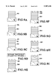
- FIG. 1A illustrates the multilayer dielectric grating concept.
- FIG. 1B shows a multilayer dielectric grating with deep ( ⁇ 300 nm) grooves which exhibits over 97% diffraction efficiency at 1053 nm.
- FIG. 2 shows a prior art high efficiency metallic grating.
- FIG. 3 shows a prior art low efficiency grating on transparent substrate.
- FIG. 4 shows a prior art low efficiency ( ⁇ 0.1%) multilayer dielectric grating concept where a multilayer stack is applied over a surface relief profile.
- FIG. 5 shows a prior art low efficiency ( ⁇ 0.1%) multilayer grating where a shallow surface relief profile is produced in the second layer (from the top) and then overcoated with one or more layers.
- FIG. 6 shows the operation of a variable efficiency multilayer dielectric grating.
- FIGS. 7A-E show the steps for fabricating a multilayer dielectric grating with deposition of the top dielectric (groove) layer through a free standing mask.
- FIGS. 8A-F show the steps for fabricating a multilayer dielectric grating by using a "lift-off" process.
- FIG. 9A-I show the steps for fabricating a multilayer dielectric grating with a chemical (wet) etch process.
- the invention is a new type of variable efficiency diffraction grating formed from purely dielectric materials.
- the grating can achieve high diffraction efficiency in reflection or transmission over an adjustable bandwidth and angle of use and can be manufactured to exhibit substantially increased resistance to optical damage over prior art metallic gratings.
- a multilayer oxide stack is placed on a substrate which in general may be composed of transparent or opaque material of any geometry (e.g., flat or curved).
- the dielectric stack will normally consist of alternating layers of high and low index dielectric materials (e.g., HfO 2 , SiO 2 , Ta 2 O 4-5 , Sc 2 O 3 , ZrO 2 , TiO 2 , Al 2 O 3 , MgF 2 , CaF 2 , ThF 4 , ZnS, ZnSe, etc.) which exhibit low absorption at the wavelength of use.
- high and low index dielectric materials e.g., HfO 2 , SiO 2 , Ta 2 O 4-5 , Sc 2 O 3 , ZrO 2 , TiO 2 , Al 2 O 3 , MgF 2 , CaF 2 , ThF 4 , ZnS, ZnSe, etc.
- grating 2 is affixed onto the top layer of layer of the dielectric stack 4.
- the multilayer structure 4 must be designed for use with the grating layer 2 under consideration since the grating layer 2 will comprise one of the layers of the multilayer stack 4.
- the multilayer stack 4 is affixed to a substrate 8.
- FIG. 1A shows groove height 10 and top layer thickness 12.
- FIG. 1B shows a multilayer dielectric grating 14 with deep ( ⁇ 300) grooves which exhibits over 97% diffraction efficiency at 1053 nm.
- FIG. 6 shows the operation of a multilayer dielectric grating of the present invention having a multilayer section 60, a substrate 62, and a surface normal 64 to the multilayer section 62 and the grating layer 63 of multilayer section 60.
- the grating can be designed to distribute the amount of radiation in the reflected, transmitted and diffracted beams as desired.
- incident beam 66 having an angle ⁇ in with respect to the normal 64, is incident upon the grating layer 63.
- a reflected diffracted beam 67' at m ⁇ 0
- a transmitted beam 68 at m 0
- the distribution of energy between the reflected, transmitted and diffracted beams can be arbitrarily controlled.
- These gratings can be fabricated by controlled deposition techniques or directly in photosensitive material as shown in FIGS. 7-9.
- the multilayer stack is designed for use with the top grating layer.
- the multilayer dielectric is then produced on top of a substrate which may be either reflecting, transparent, or opaque to the wavelength of interest.
- the initial multilayer dielectric stack is formed by any conventional coating method including but not limited to: electron beam evaporation, chemical vapor deposition, and molecular beam epitaxy.
- a multilayer dielectric coating 70 is affixed to a substrate 71 (FIG. 7A).
- a free standing deposition mask 73 is produced (FIG. 7B) and placed above the multilayer dielectric stack 70 (FIG. 7C) using spacers 73'.
- the mask 73 consists of periodic open and closed regions (lines) and may be made from any conventional means including but not limited to: e-beam lithography, x-ray, ultraviolet lithography, visible lithography, anisotropic etching of crystals, ion milling or conventional mechanical cutting.
- the grating is then formed by directional evaporation of the dielectric grating material 74 through the mask 73 (FIG.
- the open regions of the mask allow dielectric material to flow through the mask 73 and deposit on top of the multilayer stack 70.
- the closed regions of the mask block the deposition.
- the mask 73 is then removed by chemical, plasma or physical means (FIG. 7E) leaving a completed grating 75. Removal of the mask also removes the dielectric material which deposited on top of the closed regions of the mask. The result is a multilayer dielectric grating where the groove structure is in the top layer.
- a second technique which is particularly useful for non-laser applications or low power laser use is to produce the top layer directly in photoresist.
- photoresist materials are nearly completely transparent over a broad spectral range, from as short as 200 nm to as long as 1400 nm.
- these, typically organic based, dielectrics serve quite nicely as the top layer in a multilayer dielectric grating.
- the initial multilayer stack is produced by conventional techniques.
- An antireflective or absorbing layer may be placed on top of the multilayer before photoresist coating if necessary to minimize the reflectance of any radiation from the multilayer stack or mask layer during photoresist exposure.
- Photosensitive material (commonly positive or negative photoresist) is then coated at the appropriate thickness either directly on the multilayer dielectric stack or on top of the absorbing/ antireflective layer.
- the photosensitive material is then exposed to the grating pattern.
- the pattern can be produced either via exposure through a mask or by interference (holographic) techniques.
- the photoresist is chemically developed to produce a surface relief grating. By controlling the thickness of photoresist, exposure level and development process, grooves of the appropriate depth are readily produced.
- the completed grating can be baked or post-processed by other means to remove any residual solvents or unwanted chemical species. This process would correspond to stopping at step D of the lift-off process schematic shown in FIG. 8.
- Multilayer dielectric gratings have been produced by this method using several photoresists and have demonstrated a diffraction efficiency in reflection as high as 96.7% with a photoresist grating fabricated on top of a hafnium oxide/silicon oxide multilayer consisting of 8 pairs of near quarter-wave layers of alternating high index (n ⁇ 2.0, HfO 2 ) and low index (n ⁇ 1.5, SiO 2 ) material deposited on borosilicate glass.
- the "lift-off" technique is shown in FIGS. 8A-F.
- the initial multilayer dielectric stack 80 is produced by conventional means and affixed to substrate 81 (FIG. 8A).
- An antireflective or absorbing layer may be placed on top of the multilayer 80 before photoresist coating if necessary to minimize the reflectance of any radiation from the multilayer stack or mask layer during photoresist exposure.
- Photosensitive material (photoresist) 82 is then coated at the appropriate thickness either directly on the multilayer dielectric stack or on top of the absorbing/antireflective layer.
- the photosensitive material is then exposed to the grating pattern (FIG. 8C).
- the pattern can be produced either via exposure through a mask or by interference (holographic) techniques.
- the photoresist is chemically developed to produce a surface relief grating 83 (FIG. 8D).
- the surface relief pattern 83 in photoresist may need to be steepened.
- the slope of the sidewalls of the photoresist can be increased to vertical or even undercut by several methods, including but not limited to:
- the dielectric grating material 84 is deposited on the substrate by unidirectional electron-beam evaporation (or other suitably unidirectional deposition technique) (FIG. 8E).
- the equipment used for this deposition can be the same equipment used to deposit the original multilayer stack.
- the depth of the grating grooves will be determined by the thickness of dielectric material deposited.
- the original photoresist grating mask 84 can be removed ("lifted-off") by chemical dissolution or plasma means.
- the dielectric material comprising the grooves may or may not be identical to the top layer of the planar stack.
- FIGS. 9A-L The use of a chemical (wet) etch process for fabrication of a grating of the present invention is shown in FIGS. 9A-L.
- a multilayer thin film dielectric coating 90 is affixed to a substrate 91 (FIG. 9A).
- An etch mask layer 92 is then coated onto the top layer of the multilayer dielectric coating 90 (FIG. 9B).
- Photosensitive material (photoresist) 93 is then coated onto the etch mask layer 92 (FIG. 9C).
- the photoresist 93 is exposed to a grating pattern (FIG. 9D), and upon development, results in a grating pattern 94 in the photoresist (9E).
- the unprotected etch mask 95 and photoresist 96 are removed by either chemical or plasma means (FIGS. 9F-9G).
- the top layer of dielectric multilayer 90 is etched with a chemical (wet) process (FIG. 9H). Once the dielectric layer is etched to the appropriate depth, the etch mask is removed to result in a competed multilayer dielectric grating 97 (FIG. 9I).
- Grating cavity configurations as employed previously in dye laser systems have not been possible with high power density lasers (e.g. solid-state) due to the inability of conventional metallic gratings to withstand the high power density.
- This new type of grating will also extend high efficiency diffracting structures far into the ultraviolet (to below 220 nm) where the reflectivity of metallic coatings drops precipitously.
- Another unique feature of these gratings is the ability to arbitrarily adjust the bandwidth and angle of use of the grating. Since the efficiency of the grating is determined by the angle of incidence, the grating structure and the multilayer structure, the optical bandwidth and efficiency of the grating is adjustable. Some frequency components can be reflected, some transmitted, and others diffracted in either reflection, transmission, or both. This provides extreme selectivity not possible with conventional metallic or bulk dielectric transmission gratings. The optical selectivity makes it possible to select a narrow spectral region with the grating while discriminating against all others. This feature will find immediate use in high contrast spectrometers where discrimination of 10 -6 (1 part per million) is often required and is currently achieved by the use of multiple conventional gratings and/or interference filters.
- the spectral selectivity feature of these gratings will also find use as discrimination filters.
- the gratings can be designed to reflect narrow line undesirable optical radiation (e.g., laser radiation) while transmitting most other frequencies.
- An example of such an application would be to form eyeware from a multilayer grating such that the grating would transmit visible radiation and reflect (with high efficiency) unwanted radiation present from laser weapons or laser guidance systems.
- these devices can be used as selective beam splitters for use in optical switches, distribution and projection systems (e.g., head-up or flat-panel displays).
Abstract
Description
Claims (19)
Priority Applications (1)
| Application Number | Priority Date | Filing Date | Title |
|---|---|---|---|
| US08/536,874 US5907436A (en) | 1995-09-29 | 1995-09-29 | Multilayer dielectric diffraction gratings |
Applications Claiming Priority (1)
| Application Number | Priority Date | Filing Date | Title |
|---|---|---|---|
| US08/536,874 US5907436A (en) | 1995-09-29 | 1995-09-29 | Multilayer dielectric diffraction gratings |
Publications (1)
| Publication Number | Publication Date |
|---|---|
| US5907436A true US5907436A (en) | 1999-05-25 |
Family
ID=24140279
Family Applications (1)
| Application Number | Title | Priority Date | Filing Date |
|---|---|---|---|
| US08/536,874 Expired - Lifetime US5907436A (en) | 1995-09-29 | 1995-09-29 | Multilayer dielectric diffraction gratings |
Country Status (1)
| Country | Link |
|---|---|
| US (1) | US5907436A (en) |
Cited By (183)
| Publication number | Priority date | Publication date | Assignee | Title |
|---|---|---|---|---|
| USRE37473E1 (en) * | 1997-08-20 | 2001-12-18 | Imation Corp. | Diffraction anomaly sensor having grating coated with protective dielectric layer |
| US6351443B1 (en) * | 1999-11-04 | 2002-02-26 | Industrial Technology Research Institute | Diffractive stack pickup head for optical disk drives and method to fabricate the pickup head |
| US6392792B1 (en) | 2000-12-05 | 2002-05-21 | The Regents Of The University Of California | Method of fabricating reflection-mode EUV diffraction elements |
| US6424436B1 (en) * | 1999-04-06 | 2002-07-23 | Nec Corporation | Holographic element |
| US6445456B2 (en) * | 1996-12-17 | 2002-09-03 | Dr. Johannas Heidenhain Gmbh | Photoelectric position measuring device |
| US6506670B2 (en) * | 2001-05-25 | 2003-01-14 | Lsi Logic Corporation | Self aligned gate |
| US20030099038A1 (en) * | 2001-11-28 | 2003-05-29 | Hitachi Metals, Ltd. | Thin film filter for optical multiplexer/demultiplexer |
| US20030104206A1 (en) * | 2001-07-31 | 2003-06-05 | Flex Products, Inc. | Diffractive pigment flakes and compositions |
| US6577786B1 (en) | 2000-06-02 | 2003-06-10 | Digital Lightwave, Inc. | Device and method for optical performance monitoring in an optical communications network |
| US20030224164A1 (en) * | 2002-05-31 | 2003-12-04 | Flex Products, Inc., A Jds Uniphase Company | All-dielectric optical diffractive pigments |
| US20040094850A1 (en) * | 1999-07-08 | 2004-05-20 | Bonkowski Richard L. | Methods for forming security articles having diffractive surfaces and color shifting backgrounds |
| US6739728B2 (en) | 2002-04-08 | 2004-05-25 | The Regents Of The University Of California | Short pulse laser stretcher-compressor using a single common reflective grating |
| US20040130787A1 (en) * | 2002-12-19 | 2004-07-08 | Heidi Thome-Forster | Method for generating electromagnetic field distributions |
| US20040169929A1 (en) * | 2001-09-13 | 2004-09-02 | Asahi Glass Company Limited | Diffraction element |
| US20040183220A1 (en) * | 2003-03-18 | 2004-09-23 | Avinash Dalmia | Ultra thin layer coating using self-assembled molecules as a separating layer for diffraction grating application |
| US20040190141A1 (en) * | 2003-03-27 | 2004-09-30 | The Regents Of The University Of California | Durable silver thin film coating for diffraction gratings |
| US20040189284A1 (en) * | 2003-02-04 | 2004-09-30 | Mann & Hummel Gmbh | Actuator element with position detection |
| US20040196556A1 (en) * | 2000-06-02 | 2004-10-07 | Cappiello Gregory G. | Diffraction grating for wavelength division multiplexing/demultiplexing devices |
| US6809864B2 (en) * | 2001-06-29 | 2004-10-26 | Osmic, Inc | Multi-layer structure with variable bandpass for monochromatization and spectroscopy |
| US20040253426A1 (en) * | 2001-10-04 | 2004-12-16 | Andrey Yakshin | Optical element and method for its manufacture as well as lightography apparatus and method for manufacturing a semiconductor device |
| DE10327963A1 (en) * | 2003-06-19 | 2005-01-05 | Carl Zeiss Jena Gmbh | Polarization beam splitter for microscopy or projection system or UV lithography using grid array with parallel grid lines formed by multi-layer system with alternating non-metallic dielectric layers with differing optical characteristics |
| DE10341596A1 (en) * | 2003-09-05 | 2005-04-14 | Carl Zeiss | Polarization beam splitter having a high frequency grid for use in polarization and projection optics where the thickness of the grid layers are selected depending on the wavelength and angle of incident light |
| US20050088744A1 (en) * | 2003-01-06 | 2005-04-28 | Polychromix Corporation | Diffraction grating having high throughput efficiency |
| US20050132929A1 (en) * | 2002-05-31 | 2005-06-23 | Flex Products, Inc., A Jds Uniphase Company | All-dielectric optically variable pigments |
| WO2005062084A1 (en) * | 2003-12-19 | 2005-07-07 | Carl Zeiss Sms Gmbh | Element for spectral-selective beam positioning in optical appliances |
| US20050199582A1 (en) * | 2004-03-09 | 2005-09-15 | Alps Electric Co., Ltd. | Method for forming fine grating |
| US20050231806A1 (en) * | 2004-03-17 | 2005-10-20 | General Atomics | Method for making large scale multilayer dielectric diffraction gratings on thick substrates using reactive ion etching |
| EP1602947A1 (en) * | 2003-03-13 | 2005-12-07 | Asahi Glass Company Ltd. | Diffraction element and optical device |
| US20060023309A1 (en) * | 1995-12-14 | 2006-02-02 | Mitsubishi Denki Kabushiki Kaisha | Projection aligner, aberration estimating mask pattern, aberration quantity estimating method, aberration eliminating filter and semiconductor manufacturing method |
| US20060035080A1 (en) * | 2002-09-13 | 2006-02-16 | Jds Uniphase Corporation | Provision of frames or borders around opaque flakes for covert security applications |
| DE102004041222A1 (en) * | 2004-08-26 | 2006-03-02 | Carl Zeiss Jena Gmbh | Photonic crystal structure, for a frequency selective reflector or diffractive polarization-dependent band splitter, has grate bars on a substrate of alternating low and high refractive material layers |
| US20060077496A1 (en) * | 1999-07-08 | 2006-04-13 | Jds Uniphase Corporation | Patterned structures with optically variable effects |
| US20060194040A1 (en) * | 2002-09-13 | 2006-08-31 | Jds Uniphase Corporation | Two-step method of coating an article for security printing |
| US20060198998A1 (en) * | 2002-07-15 | 2006-09-07 | Jds Uniphase Corporation | Dynamic appearance-changing optical devices (dacod) printed in a shaped magnetic field including printable fresnel structures |
| US20060221440A1 (en) * | 2005-03-29 | 2006-10-05 | Asml Netherlands B.V. | Multi-layer spectral purity filter, lithographic apparatus including such a spectral purity filter, device manufacturing method, and device manufactured thereby |
| US20060263539A1 (en) * | 2002-07-15 | 2006-11-23 | Jds Uniphase Corporation | Alignable Diffractive Pigment Flakes And Method And Apparatus For Alignment And Images Formed Therefrom |
| US20060268415A1 (en) * | 2005-05-26 | 2006-11-30 | Chun-Chung Huang | Anti-reflection coating layer and design method thereof |
| US20070014017A1 (en) * | 2002-12-19 | 2007-01-18 | Oc Oerlikon Balzers Ag | Method for generating electromagnetic field distributions |
| US20070058227A1 (en) * | 1999-07-08 | 2007-03-15 | Jds Uniphase Corporation | Patterned Optical Structures With Enhanced Security Feature |
| US7199924B1 (en) | 2005-01-26 | 2007-04-03 | Aculight Corporation | Apparatus and method for spectral-beam combining of high-power fiber lasers |
| US20070091948A1 (en) * | 2005-07-29 | 2007-04-26 | Aculight Corporation | Multi-stage optical amplifier having photonic-crystal waveguides for generation of high-power pulsed radiation and associated method |
| US20070127123A1 (en) * | 2005-01-26 | 2007-06-07 | Brown Andrew J W | Method and apparatus for spectral-beam combining of high-power fiber lasers |
| US20070139744A1 (en) * | 2002-09-13 | 2007-06-21 | Jds Uniphase Corporation | Security Device With Metameric Features Using Diffractive Pigment Flakes |
| US20070172261A1 (en) * | 2002-07-15 | 2007-07-26 | Jds Uniphase Corporation | Apparatus For Orienting Magnetic Flakes |
| US20070183047A1 (en) * | 2000-01-21 | 2007-08-09 | Jds Uniphase Corporation | Optically Variable Security Devices |
| US20070195392A1 (en) * | 1999-07-08 | 2007-08-23 | Jds Uniphase Corporation | Adhesive Chromagram And Method Of Forming Thereof |
| US20070230534A1 (en) * | 2006-03-29 | 2007-10-04 | The Regents Of The University Of California | Grating enhanced solid-state laser amplifiers |
| WO2007111985A2 (en) * | 2006-03-24 | 2007-10-04 | Goodrich Corporation | Optical diffraction grating and method of manufacture |
| US20070273142A1 (en) * | 2004-04-03 | 2007-11-29 | Ovd Kinegram Ag | Security element provided in the form of a multilayered film body |
| US20080003413A1 (en) * | 2002-09-13 | 2008-01-03 | Jds Uniphase Corporation | Stamping A Coating Of Cured Field Aligned Special Effect Flakes And Image Formed Thereby |
| US20080019924A1 (en) * | 2003-08-14 | 2008-01-24 | Jds Uniphase Corporation | Non-Toxic Flakes For Authentication Of Pharmaceutical Articles |
| US20080037604A1 (en) * | 2006-03-03 | 2008-02-14 | Aculight Corporation | Diode-laser-pump module with integrated signal ports for pumping amplifying fibers and method |
| CN100386653C (en) * | 2003-03-13 | 2008-05-07 | 旭硝子株式会社 | Diffraction element and optical device |
| US20080107856A1 (en) * | 2002-09-13 | 2008-05-08 | Jds Uniphase Corporation | Provision of Frames Or Borders Around Pigment Flakes For Covert Security Applications |
| US20080137194A1 (en) * | 2004-05-07 | 2008-06-12 | Csem Centre Suisse D'electronique Et De Microtechn | Diffractive Filter |
| US20080147045A1 (en) * | 2003-06-12 | 2008-06-19 | Licentia Ltd. | Use of VEGF-C or VEGF-D in Reconstructive Surgery |
| US7400804B1 (en) | 2005-07-29 | 2008-07-15 | Aculight Corporation | Monolithic or ribbon-like multi-core photonic-crystal fibers and associated method |
| US20080171144A1 (en) * | 2002-09-13 | 2008-07-17 | Jds Uniphase Corporation | Printed Magnetic Ink Overt Security Image |
| US20080266663A1 (en) * | 2007-04-26 | 2008-10-30 | Raytheon Company | Optical pulse-width modifier structure |
| US20090028206A1 (en) * | 2005-02-22 | 2009-01-29 | Stefan Borneis | Method of Increasing the Laser Damage Threshold of Diffraction Gratings |
| US20090034576A1 (en) * | 2007-08-03 | 2009-02-05 | Newport Corporation | Linewidth-narrowed excimer laser cavity |
| US20090059375A1 (en) * | 2007-08-27 | 2009-03-05 | John Hoose | Grating Device with Adjusting Layer |
| FR2921498A1 (en) * | 2007-09-25 | 2009-03-27 | Commissariat Energie Atomique | DISPERSIVE OPTICAL DEVICE WITH THREE DIMENSIONAL PHOTONIC CRYSTAL. |
| US20090097522A1 (en) * | 2006-02-03 | 2009-04-16 | John Justice | Vertical cavity surface emitting laser device |
| US20090153880A1 (en) * | 2004-11-22 | 2009-06-18 | Koninklijke Philips Electronics, N.V. | Optical system for detecting motion of a body |
| DE112007002368T5 (en) | 2006-10-05 | 2009-09-03 | Northrop Grumman Corp., Los Angeles | Method and system for diffractive hybrid combination of coherent and incoherent beams by a beamformer |
| US20090244702A1 (en) * | 2008-03-27 | 2009-10-01 | Naotada Okada | Reflective screen, display device, and mobile apparatus |
| US20090268295A1 (en) * | 2008-04-25 | 2009-10-29 | John Michael Miller | Surface-relief diffraction grating |
| WO2010030268A1 (en) * | 2008-09-09 | 2010-03-18 | John Hoose | Grating device with adjusting layer |
| US20100208346A1 (en) * | 2009-02-13 | 2010-08-19 | Britten Jerald A | Multilayer Dielectric Transmission Gratings Having Maximal Transmitted Diffraction Efficiency |
| US20100208351A1 (en) * | 2002-07-15 | 2010-08-19 | Nofi Michael R | Selective and oriented assembly of platelet materials and functional additives |
| WO2010101829A1 (en) | 2009-03-02 | 2010-09-10 | Harris Corporation | Carbon strand radio frequency heating susceptor |
| US20110091155A1 (en) * | 2009-10-19 | 2011-04-21 | Lockheed Martin Corporation | In-line forward/backward fiber-optic signal analyzer |
| US20110103211A1 (en) * | 2009-09-08 | 2011-05-05 | Sony Corporation | Optical recording medium, method of manufacturing optical recording medium, recording method and reproducing method |
| US20110122895A1 (en) * | 2009-11-23 | 2011-05-26 | Lockheed Martin Corporation | Q-switched oscillator seed-source for mopa laser illuminator method and apparatus |
| US20110122482A1 (en) * | 2009-11-23 | 2011-05-26 | Lockheed Martin Corporation | Spectrally beam combined laser system and method at eye-safer wavelengths |
| US20110236998A1 (en) * | 2008-08-28 | 2011-09-29 | Marco Liscidini | Methods and devices for detection of analytes using bloch surface wave-enhanced diffraction-based sensors |
| CN102289014A (en) * | 2011-09-16 | 2011-12-21 | 中国科学院上海光学精密机械研究所 | Metal dielectric film reflection polarization beam splitting grating for waveband of 1,053 nanometers |
| US8089689B1 (en) | 2006-11-30 | 2012-01-03 | Lockheed Martin Corporation | Apparatus and method for optical gain fiber having segments of differing core sizes |
| CN102313920A (en) * | 2011-09-05 | 2012-01-11 | 青岛大学 | Wide spectrum metal multilayer dielectric grating based on non-normalized film structure |
| CN102314040A (en) * | 2011-09-05 | 2012-01-11 | 青岛大学 | Wide spectrum metal dielectric film grating and optimization method thereof |
| US20120044572A1 (en) * | 2009-04-20 | 2012-02-23 | Bae Systems Plc | Optical waveguides |
| US8179594B1 (en) | 2007-06-29 | 2012-05-15 | Lockheed Martin Corporation | Method and apparatus for spectral-beam combining of fanned-in laser beams with chromatic-dispersion compensation using a plurality of diffractive gratings |
| US20120120493A1 (en) * | 2009-04-20 | 2012-05-17 | Bae Systems Plc | Optical waveguides |
| EP2469324A1 (en) * | 2010-12-22 | 2012-06-27 | Delphi Technologies, Inc. | An embossed reflective volume phase grating for a heads up display system diffractive combiner |
| US20120300302A1 (en) * | 2009-12-17 | 2012-11-29 | CNRS(Centre National de la Recherche Scientifique) | Optimized dielectric reflective diffraction grating |
| DE112011101288T5 (en) | 2010-04-12 | 2013-02-07 | Lockheed Martin Corporation | Beam diagnostic and feedback system and methods for spectrally beam combined lasers |
| DE112011102811T5 (en) | 2010-08-23 | 2013-05-29 | Lockheed Martin Corporation | Fiber optic array method and apparatus |
| US20130176621A1 (en) * | 2012-01-11 | 2013-07-11 | Jds Uniphase Corporation | Diffractive mems device |
| CN103225063A (en) * | 2013-04-25 | 2013-07-31 | 中国科学院上海光学精密机械研究所 | Neodymium glass activation reflector preparation method |
| WO2013124289A1 (en) | 2012-02-21 | 2013-08-29 | Commissariat à l'énergie atomique et aux énergies alternatives | Optical reflective diffraction device having a high resistance to laser flux |
| US8526110B1 (en) | 2009-02-17 | 2013-09-03 | Lockheed Martin Corporation | Spectral-beam combining for high-power fiber-ring-laser systems |
| DE102012103443A1 (en) * | 2012-04-19 | 2013-10-24 | Fraunhofer-Gesellschaft zur Förderung der angewandten Forschung e.V. | Reflection diffraction grating and process for its production |
| US20140009590A1 (en) * | 2010-12-17 | 2014-01-09 | Celvision Technologies Limited | Display system and method thereof |
| US8658280B2 (en) | 2002-09-13 | 2014-02-25 | Jds Uniphase Corporation | Taggent flakes for covert security applications having a selected shape |
| US8750339B1 (en) | 2007-03-21 | 2014-06-10 | Lockheed Martin Corporation | Method and apparatus for high-power, pulsed ring fiber oscillator |
| US20150036218A1 (en) * | 2013-07-30 | 2015-02-05 | Northrop Grumman Systems Corporation | Hybrid diffractive optical element and spectral beam combination grating |
| US9027479B2 (en) | 2002-07-15 | 2015-05-12 | Jds Uniphase Corporation | Method and apparatus for orienting magnetic flakes |
| US9102195B2 (en) | 2012-01-12 | 2015-08-11 | Jds Uniphase Corporation | Article with curved patterns formed of aligned pigment flakes |
| WO2015124216A1 (en) * | 2014-02-24 | 2015-08-27 | Universität Stuttgart Institut für Strahlwerkzeuge | Grating mirror |
| WO2016007502A1 (en) * | 2014-07-07 | 2016-01-14 | Lumella, Inc. | Resonance enhanced diffraction grating |
| US9244281B1 (en) | 2013-09-26 | 2016-01-26 | Rockwell Collins, Inc. | Display system and method using a detached combiner |
| US9244280B1 (en) | 2014-03-25 | 2016-01-26 | Rockwell Collins, Inc. | Near eye display system and method for display enhancement or redundancy |
| US9274339B1 (en) | 2010-02-04 | 2016-03-01 | Rockwell Collins, Inc. | Worn display system and method without requiring real time tracking for boresight precision |
| US9341846B2 (en) | 2012-04-25 | 2016-05-17 | Rockwell Collins Inc. | Holographic wide angle display |
| US9366872B2 (en) | 2014-02-18 | 2016-06-14 | Lockheed Martin Corporation | Apparatus and method for fiber-laser output-beam shaping for spectral beam combination |
| US9366864B1 (en) | 2011-09-30 | 2016-06-14 | Rockwell Collins, Inc. | System for and method of displaying information without need for a combiner alignment detector |
| JP2016117185A (en) * | 2014-12-19 | 2016-06-30 | 凸版印刷株式会社 | Display body, article with display body, and authenticity determination method |
| US9383576B2 (en) | 2012-07-17 | 2016-07-05 | Rachel Andreasen | Apparatus and method for a flexible adaptive telescope mirror |
| US9429467B2 (en) | 2014-04-11 | 2016-08-30 | Lockheed Martin Corporation | System for non-contact optical-power measurement |
| US9458324B2 (en) | 2002-09-13 | 2016-10-04 | Viava Solutions Inc. | Flakes with undulate borders and method of forming thereof |
| EP3076208A1 (en) | 2015-04-04 | 2016-10-05 | Fyzikální ústav AV CR, v.v.i. | Multi-layer reflective diffraction grating and use thereof |
| US9507150B1 (en) | 2011-09-30 | 2016-11-29 | Rockwell Collins, Inc. | Head up display (HUD) using a bent waveguide assembly |
| US9519089B1 (en) | 2014-01-30 | 2016-12-13 | Rockwell Collins, Inc. | High performance volume phase gratings |
| US9523852B1 (en) | 2012-03-28 | 2016-12-20 | Rockwell Collins, Inc. | Micro collimator system and method for a head up display (HUD) |
| US9674413B1 (en) | 2013-04-17 | 2017-06-06 | Rockwell Collins, Inc. | Vision system and method having improved performance and solar mitigation |
| US9715110B1 (en) | 2014-09-25 | 2017-07-25 | Rockwell Collins, Inc. | Automotive head up display (HUD) |
| US9715067B1 (en) | 2011-09-30 | 2017-07-25 | Rockwell Collins, Inc. | Ultra-compact HUD utilizing waveguide pupil expander with surface relief gratings in high refractive index materials |
| US9720147B2 (en) | 2014-03-28 | 2017-08-01 | Lumentum Operations Llc | Reflective diffraction grating and fabrication method |
| US9835778B1 (en) | 2013-09-13 | 2017-12-05 | Lockheed Martin Corporation | Apparatus and method for a diamond substrate for a multi-layered dielectric diffraction grating |
| EP3285094A1 (en) * | 2016-08-18 | 2018-02-21 | The Boeing Company | Protective material and method for reflecting and dispersing incident energy |
| US9933684B2 (en) | 2012-11-16 | 2018-04-03 | Rockwell Collins, Inc. | Transparent waveguide display providing upper and lower fields of view having a specific light output aperture configuration |
| WO2018127684A1 (en) * | 2017-01-05 | 2018-07-12 | University Of Strathclyde | High efficiency grating |
| US10088675B1 (en) | 2015-05-18 | 2018-10-02 | Rockwell Collins, Inc. | Turning light pipe for a pupil expansion system and method |
| US20180291681A1 (en) * | 2015-10-09 | 2018-10-11 | Sharp Kabushiki Kaisha | Daylighting member, method for manufacturing daylighting member, and daylighting apparatus |
| US10108010B2 (en) | 2015-06-29 | 2018-10-23 | Rockwell Collins, Inc. | System for and method of integrating head up displays and head down displays |
| US10126552B2 (en) | 2015-05-18 | 2018-11-13 | Rockwell Collins, Inc. | Micro collimator system and method for a head up display (HUD) |
| US10156681B2 (en) | 2015-02-12 | 2018-12-18 | Digilens Inc. | Waveguide grating device |
| CN109491001A (en) * | 2018-12-12 | 2019-03-19 | 成都精密光学工程研究中心 | The unrelated grating of polarization and preparation method thereof based on covering refractive index matching layers |
| US10241244B2 (en) | 2016-07-29 | 2019-03-26 | Lumentum Operations Llc | Thin film total internal reflection diffraction grating for single polarization or dual polarization |
| US10241330B2 (en) | 2014-09-19 | 2019-03-26 | Digilens, Inc. | Method and apparatus for generating input images for holographic waveguide displays |
| US10247943B1 (en) | 2015-05-18 | 2019-04-02 | Rockwell Collins, Inc. | Head up display (HUD) using a light pipe |
| US10295824B2 (en) | 2017-01-26 | 2019-05-21 | Rockwell Collins, Inc. | Head up display with an angled light pipe |
| US10359736B2 (en) | 2014-08-08 | 2019-07-23 | Digilens Inc. | Method for holographic mastering and replication |
| US20190243034A1 (en) * | 2018-02-06 | 2019-08-08 | Raytheon Company | Low cost dispersive optical elements |
| US10495820B1 (en) | 2014-06-17 | 2019-12-03 | Lockheed Martin Corporation | Method and apparatus for low-profile fiber-coupling to photonic chips |
| US10509241B1 (en) | 2009-09-30 | 2019-12-17 | Rockwell Collins, Inc. | Optical displays |
| US10534166B2 (en) | 2016-09-22 | 2020-01-14 | Lightforce Usa, Inc. | Optical targeting information projection system |
| WO2020018270A1 (en) | 2018-07-19 | 2020-01-23 | Applied Materials, Inc. | Variable height slanted grating method |
| US10545346B2 (en) | 2017-01-05 | 2020-01-28 | Digilens Inc. | Wearable heads up displays |
| US10598932B1 (en) | 2016-01-06 | 2020-03-24 | Rockwell Collins, Inc. | Head up display for integrating views of conformally mapped symbols and a fixed image source |
| US10642058B2 (en) | 2011-08-24 | 2020-05-05 | Digilens Inc. | Wearable data display |
| US10670876B2 (en) | 2011-08-24 | 2020-06-02 | Digilens Inc. | Waveguide laser illuminator incorporating a despeckler |
| US10678053B2 (en) | 2009-04-27 | 2020-06-09 | Digilens Inc. | Diffractive projection apparatus |
| US10690916B2 (en) | 2015-10-05 | 2020-06-23 | Digilens Inc. | Apparatus for providing waveguide displays with two-dimensional pupil expansion |
| US10705269B2 (en) | 2018-03-30 | 2020-07-07 | Northrop Grumman Systems Corporation | Fabrication method of a diffractive optic for hybrid coherent and spectral beam combination |
| US10725312B2 (en) | 2007-07-26 | 2020-07-28 | Digilens Inc. | Laser illumination device |
| WO2020109225A3 (en) * | 2018-11-29 | 2020-07-30 | Carl Zeiss Smt Gmbh | Mirror for an illumination optical unit of a projection exposure apparatus comprising a spectral filter in the form of a grating structure and method for producing a spectral filter in the form of a grating structure on a mirror |
| US10732569B2 (en) | 2018-01-08 | 2020-08-04 | Digilens Inc. | Systems and methods for high-throughput recording of holographic gratings in waveguide cells |
| US10732407B1 (en) | 2014-01-10 | 2020-08-04 | Rockwell Collins, Inc. | Near eye head up display system and method with fixed combiner |
| US10747982B2 (en) | 2013-07-31 | 2020-08-18 | Digilens Inc. | Method and apparatus for contact image sensing |
| US10795160B1 (en) | 2014-09-25 | 2020-10-06 | Rockwell Collins, Inc. | Systems for and methods of using fold gratings for dual axis expansion |
| US10859768B2 (en) | 2016-03-24 | 2020-12-08 | Digilens Inc. | Method and apparatus for providing a polarization selective holographic waveguide device |
| US10890707B2 (en) | 2016-04-11 | 2021-01-12 | Digilens Inc. | Holographic waveguide apparatus for structured light projection |
| US10914950B2 (en) | 2018-01-08 | 2021-02-09 | Digilens Inc. | Waveguide architectures and related methods of manufacturing |
| CN112382858A (en) * | 2020-10-23 | 2021-02-19 | 西安理工大学 | Light-adjustable four-frequency-band terahertz metamaterial absorber based on all-dielectric material |
| US10942430B2 (en) | 2017-10-16 | 2021-03-09 | Digilens Inc. | Systems and methods for multiplying the image resolution of a pixelated display |
| US10955669B2 (en) | 2017-07-18 | 2021-03-23 | Google Llc | Systems, devices, and methods for embedding a diffractive element in an eyeglass lens |
| US11230127B2 (en) | 2002-07-15 | 2022-01-25 | Viavi Solutions Inc. | Method and apparatus for orienting magnetic flakes |
| US11256155B2 (en) | 2012-01-06 | 2022-02-22 | Digilens Inc. | Contact image sensor using switchable Bragg gratings |
| US11300795B1 (en) | 2009-09-30 | 2022-04-12 | Digilens Inc. | Systems for and methods of using fold gratings coordinated with output couplers for dual axis expansion |
| US11307432B2 (en) | 2014-08-08 | 2022-04-19 | Digilens Inc. | Waveguide laser illuminator incorporating a Despeckler |
| US11314084B1 (en) | 2011-09-30 | 2022-04-26 | Rockwell Collins, Inc. | Waveguide combiner system and method with less susceptibility to glare |
| US11320571B2 (en) | 2012-11-16 | 2022-05-03 | Rockwell Collins, Inc. | Transparent waveguide display providing upper and lower fields of view with uniform light extraction |
| US11366316B2 (en) | 2015-05-18 | 2022-06-21 | Rockwell Collins, Inc. | Head up display (HUD) using a light pipe |
| US11378732B2 (en) | 2019-03-12 | 2022-07-05 | DigLens Inc. | Holographic waveguide backlight and related methods of manufacturing |
| US11402801B2 (en) | 2018-07-25 | 2022-08-02 | Digilens Inc. | Systems and methods for fabricating a multilayer optical structure |
| US11442222B2 (en) | 2019-08-29 | 2022-09-13 | Digilens Inc. | Evacuated gratings and methods of manufacturing |
| CN115097559A (en) * | 2018-01-09 | 2022-09-23 | 瓦里安半导体设备公司 | System for generating angled grating and method for forming diffractive optical element with variable grating |
| US11487131B2 (en) | 2011-04-07 | 2022-11-01 | Digilens Inc. | Laser despeckler based on angular diversity |
| US11513350B2 (en) | 2016-12-02 | 2022-11-29 | Digilens Inc. | Waveguide device with uniform output illumination |
| US11513268B2 (en) * | 2017-06-02 | 2022-11-29 | Dispelix Oy | Method of manufacturing a variable efficiency diffractive grating and a diffractive grating |
| US11543594B2 (en) | 2019-02-15 | 2023-01-03 | Digilens Inc. | Methods and apparatuses for providing a holographic waveguide display using integrated gratings |
| US11681143B2 (en) | 2019-07-29 | 2023-06-20 | Digilens Inc. | Methods and apparatus for multiplying the image resolution and field-of-view of a pixelated display |
| US11693167B2 (en) | 2017-05-30 | 2023-07-04 | Lawrence Livermore National Security, Llc | System and method for improving the laser damage threshold of multilayer dielectric gratings |
| US11726329B2 (en) | 2015-01-12 | 2023-08-15 | Digilens Inc. | Environmentally isolated waveguide display |
| US11726332B2 (en) | 2009-04-27 | 2023-08-15 | Digilens Inc. | Diffractive projection apparatus |
| US11747568B2 (en) | 2019-06-07 | 2023-09-05 | Digilens Inc. | Waveguides incorporating transmissive and reflective gratings and related methods of manufacturing |
| US11757248B2 (en) | 2019-07-19 | 2023-09-12 | Raytheon Company | System and method for spectral line shape optimization for spectral beam combining of fiber lasers |
| US11768321B2 (en) | 2000-01-21 | 2023-09-26 | Viavi Solutions Inc. | Optically variable security devices |
| US11815705B2 (en) | 2017-06-02 | 2023-11-14 | Lawrence Livermore National Security, Llc | Innovative solutions for improving laser damage performance of multi-layer dielectric gratings |
| US11835743B2 (en) | 2017-06-02 | 2023-12-05 | Lawrence Livermore National Security, Llc | Innovative solutions to improve laser damage thresholds of optical structures |
| US11927780B2 (en) | 2022-05-31 | 2024-03-12 | National Chung Shan Institute Of Science And Technology | Dielectric grating apparatus |
Citations (10)
| Publication number | Priority date | Publication date | Assignee | Title |
|---|---|---|---|---|
| US4068260A (en) * | 1976-02-20 | 1978-01-10 | Minolta Camera Kabushiki Kaisha | Combination optical low pass filter capable of phase and amplitude modulation |
| US4155627A (en) * | 1976-02-02 | 1979-05-22 | Rca Corporation | Color diffractive subtractive filter master recording comprising a plurality of superposed two-level relief patterns on the surface of a substrate |
| US4281894A (en) * | 1980-01-21 | 1981-08-04 | The Perkin-Elmer Corporation | Very low absorption, low efficiency laser beamsampler |
| US4313648A (en) * | 1977-04-30 | 1982-02-02 | Tokyo Shibaura Denki Kabushiki Kaisha | Patterned multi-layer structure and manufacturing method |
| US4330175A (en) * | 1978-07-18 | 1982-05-18 | Nippon Telegraph & Telephone Public Corporation | Blazed diffraction grating structures and method of manufacturing the same |
| US4482207A (en) * | 1981-06-29 | 1984-11-13 | Dynamics Research Corporation | Optical grating and method of manufacture |
| US4828356A (en) * | 1987-12-22 | 1989-05-09 | Hughes Aircraft Company | Method for fabrication of low efficiency diffraction gratings and product obtained thereby |
| US5009484A (en) * | 1989-05-03 | 1991-04-23 | Advanced Environmental Research Group | Diffraction gratings having high efficiencies |
| US5219788A (en) * | 1991-02-25 | 1993-06-15 | Ibm Corporation | Bilayer metallization cap for photolithography |
| US5254202A (en) * | 1992-04-07 | 1993-10-19 | International Business Machines Corporation | Fabrication of laser ablation masks by wet etching |
-
1995
- 1995-09-29 US US08/536,874 patent/US5907436A/en not_active Expired - Lifetime
Patent Citations (10)
| Publication number | Priority date | Publication date | Assignee | Title |
|---|---|---|---|---|
| US4155627A (en) * | 1976-02-02 | 1979-05-22 | Rca Corporation | Color diffractive subtractive filter master recording comprising a plurality of superposed two-level relief patterns on the surface of a substrate |
| US4068260A (en) * | 1976-02-20 | 1978-01-10 | Minolta Camera Kabushiki Kaisha | Combination optical low pass filter capable of phase and amplitude modulation |
| US4313648A (en) * | 1977-04-30 | 1982-02-02 | Tokyo Shibaura Denki Kabushiki Kaisha | Patterned multi-layer structure and manufacturing method |
| US4330175A (en) * | 1978-07-18 | 1982-05-18 | Nippon Telegraph & Telephone Public Corporation | Blazed diffraction grating structures and method of manufacturing the same |
| US4281894A (en) * | 1980-01-21 | 1981-08-04 | The Perkin-Elmer Corporation | Very low absorption, low efficiency laser beamsampler |
| US4482207A (en) * | 1981-06-29 | 1984-11-13 | Dynamics Research Corporation | Optical grating and method of manufacture |
| US4828356A (en) * | 1987-12-22 | 1989-05-09 | Hughes Aircraft Company | Method for fabrication of low efficiency diffraction gratings and product obtained thereby |
| US5009484A (en) * | 1989-05-03 | 1991-04-23 | Advanced Environmental Research Group | Diffraction gratings having high efficiencies |
| US5219788A (en) * | 1991-02-25 | 1993-06-15 | Ibm Corporation | Bilayer metallization cap for photolithography |
| US5254202A (en) * | 1992-04-07 | 1993-10-19 | International Business Machines Corporation | Fabrication of laser ablation masks by wet etching |
Non-Patent Citations (2)
| Title |
|---|
| J. M. Elson, Infrared light scattering surfaces covered with multiple dielectric overlays, Dec. 18, 1975, Applied Optics, vol. 16, No. 11, Nov. 1977, pp. 2872 2881. * |
| J. M. Elson, Infrared light scattering surfaces covered with multiple dielectric overlays, Dec. 18, 1975, Applied Optics, vol. 16, No. 11, Nov. 1977, pp. 2872-2881. |
Cited By (335)
| Publication number | Priority date | Publication date | Assignee | Title |
|---|---|---|---|---|
| US20060023309A1 (en) * | 1995-12-14 | 2006-02-02 | Mitsubishi Denki Kabushiki Kaisha | Projection aligner, aberration estimating mask pattern, aberration quantity estimating method, aberration eliminating filter and semiconductor manufacturing method |
| US7170682B2 (en) * | 1995-12-14 | 2007-01-30 | Renesas Technology Corp. | Projection aligner, aberration estimating mask pattern, aberration quantity estimating method, aberration eliminating filter and semiconductor manufacturing method |
| US6445456B2 (en) * | 1996-12-17 | 2002-09-03 | Dr. Johannas Heidenhain Gmbh | Photoelectric position measuring device |
| USRE37473E1 (en) * | 1997-08-20 | 2001-12-18 | Imation Corp. | Diffraction anomaly sensor having grating coated with protective dielectric layer |
| US6424436B1 (en) * | 1999-04-06 | 2002-07-23 | Nec Corporation | Holographic element |
| US7876481B2 (en) | 1999-07-08 | 2011-01-25 | Jds Uniphase Corporation | Patterned optical structures with enhanced security feature |
| US20070058227A1 (en) * | 1999-07-08 | 2007-03-15 | Jds Uniphase Corporation | Patterned Optical Structures With Enhanced Security Feature |
| US20080024847A1 (en) * | 1999-07-08 | 2008-01-31 | Jds Uniphase Corporation | Patterned Optical Structures With Enhanced Security Feature |
| US20060077496A1 (en) * | 1999-07-08 | 2006-04-13 | Jds Uniphase Corporation | Patterned structures with optically variable effects |
| US7667895B2 (en) | 1999-07-08 | 2010-02-23 | Jds Uniphase Corporation | Patterned structures with optically variable effects |
| US20040094850A1 (en) * | 1999-07-08 | 2004-05-20 | Bonkowski Richard L. | Methods for forming security articles having diffractive surfaces and color shifting backgrounds |
| US7754112B2 (en) | 1999-07-08 | 2010-07-13 | Jds Uniphase Corporation | Methods for forming security articles having diffractive surfaces and color shifting backgrounds |
| US20080018965A1 (en) * | 1999-07-08 | 2008-01-24 | Jds Uniphase Corporation | Diffractive Surfaces With Color Shifting Backgrounds |
| US20070292636A1 (en) * | 1999-07-08 | 2007-12-20 | Jds Uniphase Corporation. | Security Device Having A Segmented Layer |
| US7880943B2 (en) | 1999-07-08 | 2011-02-01 | Jds Uniphase Corporation | Patterned optical structures with enhanced security feature |
| US20070195392A1 (en) * | 1999-07-08 | 2007-08-23 | Jds Uniphase Corporation | Adhesive Chromagram And Method Of Forming Thereof |
| US6351443B1 (en) * | 1999-11-04 | 2002-02-26 | Industrial Technology Research Institute | Diffractive stack pickup head for optical disk drives and method to fabricate the pickup head |
| US11768321B2 (en) | 2000-01-21 | 2023-09-26 | Viavi Solutions Inc. | Optically variable security devices |
| US20070183047A1 (en) * | 2000-01-21 | 2007-08-09 | Jds Uniphase Corporation | Optically Variable Security Devices |
| US20040196556A1 (en) * | 2000-06-02 | 2004-10-07 | Cappiello Gregory G. | Diffraction grating for wavelength division multiplexing/demultiplexing devices |
| US6577786B1 (en) | 2000-06-02 | 2003-06-10 | Digital Lightwave, Inc. | Device and method for optical performance monitoring in an optical communications network |
| US6392792B1 (en) | 2000-12-05 | 2002-05-21 | The Regents Of The University Of California | Method of fabricating reflection-mode EUV diffraction elements |
| US6506670B2 (en) * | 2001-05-25 | 2003-01-14 | Lsi Logic Corporation | Self aligned gate |
| US6809864B2 (en) * | 2001-06-29 | 2004-10-26 | Osmic, Inc | Multi-layer structure with variable bandpass for monochromatization and spectroscopy |
| US9257059B2 (en) | 2001-07-31 | 2016-02-09 | Viavi Solutions Inc. | Dynamic appearance-changing optical devices (DACOD) printed in a shaped magnetic field including printable fresnel structures |
| US20030104206A1 (en) * | 2001-07-31 | 2003-06-05 | Flex Products, Inc. | Diffractive pigment flakes and compositions |
| US6749777B2 (en) * | 2001-07-31 | 2004-06-15 | Flex Products, Inc. | Diffractive pigment flakes and compositions |
| US7430076B2 (en) * | 2001-09-13 | 2008-09-30 | Asahi Glass Company, Limited | Diffraction element |
| US20080310024A1 (en) * | 2001-09-13 | 2008-12-18 | Asahi Glass Company Limited | Diffraction element |
| US20040169929A1 (en) * | 2001-09-13 | 2004-09-02 | Asahi Glass Company Limited | Diffraction element |
| US7172788B2 (en) * | 2001-10-04 | 2007-02-06 | Carl Zeiss Smt Ag | Optical element and method for its manufacture as well as lithography apparatus and method for manufacturing a semiconductor device |
| US20040253426A1 (en) * | 2001-10-04 | 2004-12-16 | Andrey Yakshin | Optical element and method for its manufacture as well as lightography apparatus and method for manufacturing a semiconductor device |
| US20030099038A1 (en) * | 2001-11-28 | 2003-05-29 | Hitachi Metals, Ltd. | Thin film filter for optical multiplexer/demultiplexer |
| US6739728B2 (en) | 2002-04-08 | 2004-05-25 | The Regents Of The University Of California | Short pulse laser stretcher-compressor using a single common reflective grating |
| US7238424B2 (en) | 2002-05-31 | 2007-07-03 | Jds Uniphase Corporation | All-dielectric optically variable pigments |
| US20030224164A1 (en) * | 2002-05-31 | 2003-12-04 | Flex Products, Inc., A Jds Uniphase Company | All-dielectric optical diffractive pigments |
| US20050132929A1 (en) * | 2002-05-31 | 2005-06-23 | Flex Products, Inc., A Jds Uniphase Company | All-dielectric optically variable pigments |
| US6815065B2 (en) * | 2002-05-31 | 2004-11-09 | Flex Products, Inc. | All-dielectric optical diffractive pigments |
| US7934451B2 (en) | 2002-07-15 | 2011-05-03 | Jds Uniphase Corporation | Apparatus for orienting magnetic flakes |
| US20060198998A1 (en) * | 2002-07-15 | 2006-09-07 | Jds Uniphase Corporation | Dynamic appearance-changing optical devices (dacod) printed in a shaped magnetic field including printable fresnel structures |
| US9522402B2 (en) | 2002-07-15 | 2016-12-20 | Viavi Solutions Inc. | Method and apparatus for orienting magnetic flakes |
| US7625632B2 (en) | 2002-07-15 | 2009-12-01 | Jds Uniphase Corporation | Alignable diffractive pigment flakes and method and apparatus for alignment and images formed therefrom |
| US20060263539A1 (en) * | 2002-07-15 | 2006-11-23 | Jds Uniphase Corporation | Alignable Diffractive Pigment Flakes And Method And Apparatus For Alignment And Images Formed Therefrom |
| US9027479B2 (en) | 2002-07-15 | 2015-05-12 | Jds Uniphase Corporation | Method and apparatus for orienting magnetic flakes |
| US20100208351A1 (en) * | 2002-07-15 | 2010-08-19 | Nofi Michael R | Selective and oriented assembly of platelet materials and functional additives |
| US10059137B2 (en) | 2002-07-15 | 2018-08-28 | Viavi Solutions Inc. | Apparatus for orienting magnetic flakes |
| US10173455B2 (en) | 2002-07-15 | 2019-01-08 | Viavi Solutions Inc. | Dynamic appearance-changing optical devices (DACOD) printed in a shaped magnetic field including printable fresnel structures |
| US8726806B2 (en) | 2002-07-15 | 2014-05-20 | Jds Uniphase Corporation | Apparatus for orienting magnetic flakes |
| US11230127B2 (en) | 2002-07-15 | 2022-01-25 | Viavi Solutions Inc. | Method and apparatus for orienting magnetic flakes |
| US8343615B2 (en) | 2002-07-15 | 2013-01-01 | Jds Uniphase Corporation | Dynamic appearance-changing optical devices (DACOD) printed in a shaped magnetic field including printable fresnel structures |
| US20070172261A1 (en) * | 2002-07-15 | 2007-07-26 | Jds Uniphase Corporation | Apparatus For Orienting Magnetic Flakes |
| US7674501B2 (en) | 2002-09-13 | 2010-03-09 | Jds Uniphase Corporation | Two-step method of coating an article for security printing by application of electric or magnetic field |
| US20060194040A1 (en) * | 2002-09-13 | 2006-08-31 | Jds Uniphase Corporation | Two-step method of coating an article for security printing |
| US20070139744A1 (en) * | 2002-09-13 | 2007-06-21 | Jds Uniphase Corporation | Security Device With Metameric Features Using Diffractive Pigment Flakes |
| US20060035080A1 (en) * | 2002-09-13 | 2006-02-16 | Jds Uniphase Corporation | Provision of frames or borders around opaque flakes for covert security applications |
| US8118963B2 (en) | 2002-09-13 | 2012-02-21 | Alberto Argoitia | Stamping a coating of cured field aligned special effect flakes and image formed thereby |
| US8999616B2 (en) | 2002-09-13 | 2015-04-07 | Jds Uniphase Corporation | Taggent flakes for covert security applications having a selected shape |
| US9458324B2 (en) | 2002-09-13 | 2016-10-04 | Viava Solutions Inc. | Flakes with undulate borders and method of forming thereof |
| USRE45762E1 (en) | 2002-09-13 | 2015-10-20 | Jds Uniphase Corporation | Printed magnetic ink overt security image |
| US7729026B2 (en) | 2002-09-13 | 2010-06-01 | Jds Uniphase Corporation | Security device with metameric features using diffractive pigment flakes |
| US20080171144A1 (en) * | 2002-09-13 | 2008-07-17 | Jds Uniphase Corporation | Printed Magnetic Ink Overt Security Image |
| US8025952B2 (en) | 2002-09-13 | 2011-09-27 | Jds Uniphase Corporation | Printed magnetic ink overt security image |
| US20080107856A1 (en) * | 2002-09-13 | 2008-05-08 | Jds Uniphase Corporation | Provision of Frames Or Borders Around Pigment Flakes For Covert Security Applications |
| US9164575B2 (en) | 2002-09-13 | 2015-10-20 | Jds Uniphase Corporation | Provision of frames or borders around pigment flakes for covert security applications |
| US8658280B2 (en) | 2002-09-13 | 2014-02-25 | Jds Uniphase Corporation | Taggent flakes for covert security applications having a selected shape |
| US20080003413A1 (en) * | 2002-09-13 | 2008-01-03 | Jds Uniphase Corporation | Stamping A Coating Of Cured Field Aligned Special Effect Flakes And Image Formed Thereby |
| US20100002275A9 (en) * | 2002-09-13 | 2010-01-07 | Jds Uniphase Corporation | Security Device With Metameric Features Using Diffractive Pigment Flakes |
| US7645510B2 (en) | 2002-09-13 | 2010-01-12 | Jds Uniphase Corporation | Provision of frames or borders around opaque flakes for covert security applications |
| US7110181B2 (en) * | 2002-12-19 | 2006-09-19 | Unaxis Balzers Ltd. | Method for generating electromagnetic field distributions |
| US20070014017A1 (en) * | 2002-12-19 | 2007-01-18 | Oc Oerlikon Balzers Ag | Method for generating electromagnetic field distributions |
| WO2004057315A1 (en) * | 2002-12-19 | 2004-07-08 | Unaxis Balzers Ag | Method for generating electromagnetic field distributions |
| US20040130787A1 (en) * | 2002-12-19 | 2004-07-08 | Heidi Thome-Forster | Method for generating electromagnetic field distributions |
| US20050088744A1 (en) * | 2003-01-06 | 2005-04-28 | Polychromix Corporation | Diffraction grating having high throughput efficiency |
| US7139128B2 (en) | 2003-01-06 | 2006-11-21 | Polychromix Corporation | Diffraction grating having high throughput efficiency |
| US20040189284A1 (en) * | 2003-02-04 | 2004-09-30 | Mann & Hummel Gmbh | Actuator element with position detection |
| US7044444B2 (en) | 2003-02-04 | 2006-05-16 | Mann & Hummel Gmbh | Actuator element with position detection |
| EP1602947A1 (en) * | 2003-03-13 | 2005-12-07 | Asahi Glass Company Ltd. | Diffraction element and optical device |
| CN100386653C (en) * | 2003-03-13 | 2008-05-07 | 旭硝子株式会社 | Diffraction element and optical device |
| EP1602947A4 (en) * | 2003-03-13 | 2007-03-28 | Asahi Glass Co Ltd | Diffraction element and optical device |
| US20040183220A1 (en) * | 2003-03-18 | 2004-09-23 | Avinash Dalmia | Ultra thin layer coating using self-assembled molecules as a separating layer for diffraction grating application |
| US20040190141A1 (en) * | 2003-03-27 | 2004-09-30 | The Regents Of The University Of California | Durable silver thin film coating for diffraction gratings |
| US7054065B2 (en) | 2003-03-27 | 2006-05-30 | The Regents Of The University Of California | Durable silver thin film coating for diffraction gratings |
| US20080147045A1 (en) * | 2003-06-12 | 2008-06-19 | Licentia Ltd. | Use of VEGF-C or VEGF-D in Reconstructive Surgery |
| DE10327963A1 (en) * | 2003-06-19 | 2005-01-05 | Carl Zeiss Jena Gmbh | Polarization beam splitter for microscopy or projection system or UV lithography using grid array with parallel grid lines formed by multi-layer system with alternating non-metallic dielectric layers with differing optical characteristics |
| US20080019924A1 (en) * | 2003-08-14 | 2008-01-24 | Jds Uniphase Corporation | Non-Toxic Flakes For Authentication Of Pharmaceutical Articles |
| US7550197B2 (en) | 2003-08-14 | 2009-06-23 | Jds Uniphase Corporation | Non-toxic flakes for authentication of pharmaceutical articles |
| DE10341596A1 (en) * | 2003-09-05 | 2005-04-14 | Carl Zeiss | Polarization beam splitter having a high frequency grid for use in polarization and projection optics where the thickness of the grid layers are selected depending on the wavelength and angle of incident light |
| DE10341596B4 (en) * | 2003-09-05 | 2009-01-29 | Carl Zeiss | Polarization beam splitter |
| WO2005062084A1 (en) * | 2003-12-19 | 2005-07-07 | Carl Zeiss Sms Gmbh | Element for spectral-selective beam positioning in optical appliances |
| KR101060184B1 (en) | 2003-12-19 | 2011-08-29 | 플렉스 프로덕츠, 인코포레이티드 | Fully-Dielectric Optically Variable Pigments |
| US20050199582A1 (en) * | 2004-03-09 | 2005-09-15 | Alps Electric Co., Ltd. | Method for forming fine grating |
| US20050231806A1 (en) * | 2004-03-17 | 2005-10-20 | General Atomics | Method for making large scale multilayer dielectric diffraction gratings on thick substrates using reactive ion etching |
| US7256938B2 (en) * | 2004-03-17 | 2007-08-14 | General Atomics | Method for making large scale multilayer dielectric diffraction gratings on thick substrates using reactive ion etching |
| US20070273142A1 (en) * | 2004-04-03 | 2007-11-29 | Ovd Kinegram Ag | Security element provided in the form of a multilayered film body |
| US8238027B2 (en) | 2004-04-03 | 2012-08-07 | Ovd Kinegram Ag | Security element provided in the form of a multilayered film body |
| US20080137194A1 (en) * | 2004-05-07 | 2008-06-12 | Csem Centre Suisse D'electronique Et De Microtechn | Diffractive Filter |
| DE102004041222A1 (en) * | 2004-08-26 | 2006-03-02 | Carl Zeiss Jena Gmbh | Photonic crystal structure, for a frequency selective reflector or diffractive polarization-dependent band splitter, has grate bars on a substrate of alternating low and high refractive material layers |
| US20090153880A1 (en) * | 2004-11-22 | 2009-06-18 | Koninklijke Philips Electronics, N.V. | Optical system for detecting motion of a body |
| US20070127123A1 (en) * | 2005-01-26 | 2007-06-07 | Brown Andrew J W | Method and apparatus for spectral-beam combining of high-power fiber lasers |
| US7233442B1 (en) | 2005-01-26 | 2007-06-19 | Aculight Corporation | Method and apparatus for spectral-beam combining of high-power fiber lasers |
| US7535631B2 (en) | 2005-01-26 | 2009-05-19 | Lockheed Martin Corporation | Method and apparatus for spectral-beam combining of fiber-amplified laser beams using high-efficiency dielectric diffractive gratings |
| US7199924B1 (en) | 2005-01-26 | 2007-04-03 | Aculight Corporation | Apparatus and method for spectral-beam combining of high-power fiber lasers |
| US20070229939A1 (en) * | 2005-01-26 | 2007-10-04 | Aculight Corporation | Method and apparatus for spectral-beam combining of fiber-amplified laser beams using high-efficiency dielectric diffractive gratings |
| US8349226B2 (en) * | 2005-02-22 | 2013-01-08 | Gsi Helmholtzzentrum Fur Schwerionenforschung Gmbh | Method of increasing the laser damage threshold of diffraction gratings |
| US20090028206A1 (en) * | 2005-02-22 | 2009-01-29 | Stefan Borneis | Method of Increasing the Laser Damage Threshold of Diffraction Gratings |
| US7372623B2 (en) * | 2005-03-29 | 2008-05-13 | Asml Netherlands B.V. | Multi-layer spectral purity filter, lithographic apparatus including such a spectral purity filter, device manufacturing method, and device manufactured thereby |
| US20080151361A1 (en) * | 2005-03-29 | 2008-06-26 | Asml Netherlands B.V. | Multi-layer spectral purity filter, lithographic apparatus including such a spectral purity filter, device manufacturing method, and device manufactured thereby |
| US20060221440A1 (en) * | 2005-03-29 | 2006-10-05 | Asml Netherlands B.V. | Multi-layer spectral purity filter, lithographic apparatus including such a spectral purity filter, device manufacturing method, and device manufactured thereby |
| US7639418B2 (en) | 2005-03-29 | 2009-12-29 | Asml Netherlands B.V. | Multi-layer spectral purity filter, lithographic apparatus including such a spectral purity filter, device manufacturing method, and device manufactured thereby |
| US20060268415A1 (en) * | 2005-05-26 | 2006-11-30 | Chun-Chung Huang | Anti-reflection coating layer and design method thereof |
| US7782527B1 (en) | 2005-07-29 | 2010-08-24 | Lockheed Martin Corporation | Multi-stage optical amplifier having photonic-crystal-rod waveguides and non-photonic-crystal optical fiber interconnects and associated method |
| US7835068B1 (en) | 2005-07-29 | 2010-11-16 | Lockheed Martin Corporation | Photonic-crystal-rod optical amplifier with sealed-hole endcap and associated method |
| US7440175B2 (en) | 2005-07-29 | 2008-10-21 | Aculight Corporation | Multi-stage optical amplifier having photonic-crystal waveguides for generation of high-power pulsed radiation and associated method |
| US7436585B1 (en) | 2005-07-29 | 2008-10-14 | Aculight Corporation | Chirped-pulse amplifier using photonic-crystal-rod (PCR) waveguides and associated method |
| US7751118B1 (en) | 2005-07-29 | 2010-07-06 | Lockheed Martin Corporation | Method and apparatus for ultra-violet-wavelength laser-induced fluorescence (UV-LIF) using optical output from a photonic-crystal rod |
| US7375877B1 (en) | 2005-07-29 | 2008-05-20 | Aculight Corporation | Method and apparatus for long-range lidar and active imaging with optical output from a photonic-crystal rod |
| US7430352B2 (en) | 2005-07-29 | 2008-09-30 | Aculight Corporation | Multi-segment photonic-crystal-rod waveguides for amplification of high-power pulsed optical radiation and associated method |
| US7400804B1 (en) | 2005-07-29 | 2008-07-15 | Aculight Corporation | Monolithic or ribbon-like multi-core photonic-crystal fibers and associated method |
| US9207408B1 (en) | 2005-07-29 | 2015-12-08 | Lockheed Martin Corporation | Laser system and method |
| US7941019B1 (en) | 2005-07-29 | 2011-05-10 | Lockheed Martin Corporation | Monolithic pump block for optical amplifiers and associated method |
| US7391561B2 (en) | 2005-07-29 | 2008-06-24 | Aculight Corporation | Fiber- or rod-based optical source featuring a large-core, rare-earth-doped photonic-crystal device for generation of high-power pulsed radiation and method |
| US20070091948A1 (en) * | 2005-07-29 | 2007-04-26 | Aculight Corporation | Multi-stage optical amplifier having photonic-crystal waveguides for generation of high-power pulsed radiation and associated method |
| US7830596B1 (en) | 2005-07-29 | 2010-11-09 | Lockheed Martin Corporation | Fiber-or rod-based optical source featuring a large-core, rare-earth-doped photonic-crystal device for generation of narrow-bandwidth high-power pulsed radiation and associated method |
| US8472763B1 (en) | 2005-07-29 | 2013-06-25 | Lockheed Martin Corporation | Spectral beam combination of laser beams |
| US7386211B1 (en) | 2005-07-29 | 2008-06-10 | Aculight Corporation | Method and apparatus for spectral-beam combining of megawatt-peak-power beams from photonic-crystal rods |
| US7379237B1 (en) | 2005-07-29 | 2008-05-27 | Aculight Corporation | Photonic-crystal-rod amplifiers for high-power pulsed optical radiation and associated method |
| US7379648B1 (en) | 2005-07-29 | 2008-05-27 | Aculight Corporation | Optical hollow-core delivery fiber and hollow-endcap termination and associated method |
| US9653872B2 (en) | 2005-10-24 | 2017-05-16 | Lockheed Martin Corporation | System and method for high-power, pulsed ring fiber oscillator |
| US20090097522A1 (en) * | 2006-02-03 | 2009-04-16 | John Justice | Vertical cavity surface emitting laser device |
| US20080037604A1 (en) * | 2006-03-03 | 2008-02-14 | Aculight Corporation | Diode-laser-pump module with integrated signal ports for pumping amplifying fibers and method |
| US7537395B2 (en) | 2006-03-03 | 2009-05-26 | Lockheed Martin Corporation | Diode-laser-pump module with integrated signal ports for pumping amplifying fibers and method |
| US20080062523A1 (en) * | 2006-03-24 | 2008-03-13 | Goodrich Corporation | Optical diffraction grating and method of manufacture |
| WO2007111985A3 (en) * | 2006-03-24 | 2007-11-22 | Goodrich Corp | Optical diffraction grating and method of manufacture |
| WO2007111985A2 (en) * | 2006-03-24 | 2007-10-04 | Goodrich Corporation | Optical diffraction grating and method of manufacture |
| US20070230534A1 (en) * | 2006-03-29 | 2007-10-04 | The Regents Of The University Of California | Grating enhanced solid-state laser amplifiers |
| US7830946B2 (en) * | 2006-03-29 | 2010-11-09 | Lawrence Livermore National Security, Llc | Grating enhanced solid-state laser amplifiers |
| DE112007002368T5 (en) | 2006-10-05 | 2009-09-03 | Northrop Grumman Corp., Los Angeles | Method and system for diffractive hybrid combination of coherent and incoherent beams by a beamformer |
| US8199399B1 (en) | 2006-11-30 | 2012-06-12 | Lockheed Martin Corporation | Optical gain fiber having segments of differing core sizes and associated method |
| US8089689B1 (en) | 2006-11-30 | 2012-01-03 | Lockheed Martin Corporation | Apparatus and method for optical gain fiber having segments of differing core sizes |
| US8345348B1 (en) | 2006-11-30 | 2013-01-01 | Lockheed Martin Corporation | Method and optical gain fiber having segments of differing core sizes |
| US8705166B1 (en) | 2006-11-30 | 2014-04-22 | Lockheed Martin Corporation | Optical gain fiber having tapered segments of differing core sizes and associated method |
| US8750339B1 (en) | 2007-03-21 | 2014-06-10 | Lockheed Martin Corporation | Method and apparatus for high-power, pulsed ring fiber oscillator |
| US20080266663A1 (en) * | 2007-04-26 | 2008-10-30 | Raytheon Company | Optical pulse-width modifier structure |
| US7589896B2 (en) | 2007-04-26 | 2009-09-15 | Raytheon Company | Optical pulse-width modifier structure |
| US8179594B1 (en) | 2007-06-29 | 2012-05-15 | Lockheed Martin Corporation | Method and apparatus for spectral-beam combining of fanned-in laser beams with chromatic-dispersion compensation using a plurality of diffractive gratings |
| US10725312B2 (en) | 2007-07-26 | 2020-07-28 | Digilens Inc. | Laser illumination device |
| US20090034576A1 (en) * | 2007-08-03 | 2009-02-05 | Newport Corporation | Linewidth-narrowed excimer laser cavity |
| WO2009020813A1 (en) * | 2007-08-03 | 2009-02-12 | Newport Corporation | Linewidth-narrowed excimer laser cavity |
| US8116002B2 (en) | 2007-08-27 | 2012-02-14 | Lumella Inc. | Grating device with adjusting layer |
| US20090059375A1 (en) * | 2007-08-27 | 2009-03-05 | John Hoose | Grating Device with Adjusting Layer |
| US9013794B2 (en) * | 2007-09-25 | 2015-04-21 | Commissariat A L'energie Atomique | Dispersive optical device with three-dimensional photonic crystal |
| US20100202057A1 (en) * | 2007-09-25 | 2010-08-12 | Commissariat A L'energie Atomique | Dispersive optical device with three-dimensional photonic crystal |
| FR2921498A1 (en) * | 2007-09-25 | 2009-03-27 | Commissariat Energie Atomique | DISPERSIVE OPTICAL DEVICE WITH THREE DIMENSIONAL PHOTONIC CRYSTAL. |
| WO2009040353A1 (en) * | 2007-09-25 | 2009-04-02 | Commissariat A L'energie Atomique | Dispersive optical device with three dimensional photonic crystal |
| US8081382B2 (en) * | 2008-03-27 | 2011-12-20 | Kabushiki Kaisha Toshiba | Reflective screen, display device, and mobile apparatus |
| US20090244702A1 (en) * | 2008-03-27 | 2009-10-01 | Naotada Okada | Reflective screen, display device, and mobile apparatus |
| US8040607B2 (en) | 2008-04-25 | 2011-10-18 | Jds Uniphase Corporation | Surface-relief diffraction grating |
| US20090268295A1 (en) * | 2008-04-25 | 2009-10-29 | John Michael Miller | Surface-relief diffraction grating |
| US9658221B2 (en) * | 2008-08-28 | 2017-05-23 | The Governing Council Of The University Of Toronto | Methods and devices for detection of analytes using bloch surface wave-enhanced diffraction-based sensors |
| US20110236998A1 (en) * | 2008-08-28 | 2011-09-29 | Marco Liscidini | Methods and devices for detection of analytes using bloch surface wave-enhanced diffraction-based sensors |
| WO2010030268A1 (en) * | 2008-09-09 | 2010-03-18 | John Hoose | Grating device with adjusting layer |
| US20100208346A1 (en) * | 2009-02-13 | 2010-08-19 | Britten Jerald A | Multilayer Dielectric Transmission Gratings Having Maximal Transmitted Diffraction Efficiency |
| US8526110B1 (en) | 2009-02-17 | 2013-09-03 | Lockheed Martin Corporation | Spectral-beam combining for high-power fiber-ring-laser systems |
| WO2010101829A1 (en) | 2009-03-02 | 2010-09-10 | Harris Corporation | Carbon strand radio frequency heating susceptor |
| US9328243B2 (en) | 2009-03-02 | 2016-05-03 | Harris Corporation | Carbon strand radio frequency heating susceptor |
| US20120044572A1 (en) * | 2009-04-20 | 2012-02-23 | Bae Systems Plc | Optical waveguides |
| US9329325B2 (en) * | 2009-04-20 | 2016-05-03 | Bae Systems Plc | Optical waveguides |
| US20120120493A1 (en) * | 2009-04-20 | 2012-05-17 | Bae Systems Plc | Optical waveguides |
| US10642039B2 (en) * | 2009-04-20 | 2020-05-05 | Bae Systems Plc | Surface relief grating in an optical waveguide having a reflecting surface and dielectric layer conforming to the surface |
| US11726332B2 (en) | 2009-04-27 | 2023-08-15 | Digilens Inc. | Diffractive projection apparatus |
| US11175512B2 (en) | 2009-04-27 | 2021-11-16 | Digilens Inc. | Diffractive projection apparatus |
| US10678053B2 (en) | 2009-04-27 | 2020-06-09 | Digilens Inc. | Diffractive projection apparatus |
| US20110103211A1 (en) * | 2009-09-08 | 2011-05-05 | Sony Corporation | Optical recording medium, method of manufacturing optical recording medium, recording method and reproducing method |
| US11300795B1 (en) | 2009-09-30 | 2022-04-12 | Digilens Inc. | Systems for and methods of using fold gratings coordinated with output couplers for dual axis expansion |
| US10509241B1 (en) | 2009-09-30 | 2019-12-17 | Rockwell Collins, Inc. | Optical displays |
| US20110091155A1 (en) * | 2009-10-19 | 2011-04-21 | Lockheed Martin Corporation | In-line forward/backward fiber-optic signal analyzer |
| US8755649B2 (en) | 2009-10-19 | 2014-06-17 | Lockheed Martin Corporation | In-line forward/backward fiber-optic signal analyzer |
| WO2011049841A1 (en) | 2009-10-19 | 2011-04-28 | Lockheed Martin Corporation | In-line forward/backward fiber-optic signal analyzer |
| US20110122895A1 (en) * | 2009-11-23 | 2011-05-26 | Lockheed Martin Corporation | Q-switched oscillator seed-source for mopa laser illuminator method and apparatus |
| US8441718B2 (en) | 2009-11-23 | 2013-05-14 | Lockheed Martin Corporation | Spectrally beam combined laser system and method at eye-safer wavelengths |
| US20110122482A1 (en) * | 2009-11-23 | 2011-05-26 | Lockheed Martin Corporation | Spectrally beam combined laser system and method at eye-safer wavelengths |
| WO2011063364A1 (en) | 2009-11-23 | 2011-05-26 | Lockheed Martin Corporation | Spectrally beam combined laser system and method for generating eye - safer wavelengths |
| US9923329B2 (en) | 2009-11-23 | 2018-03-20 | Lockheed Martin Corporation | Q-switched oscillator seed-source for MOPA laser illuminator apparatus and method |
| WO2011068712A2 (en) | 2009-11-23 | 2011-06-09 | Lockheed Martin Corporation | Q-switched oscillator seed-source for mopa laser illuminator method and apparatus |
| US8934509B2 (en) | 2009-11-23 | 2015-01-13 | Lockheed Martin Corporation | Q-switched oscillator seed-source for MOPA laser illuminator method and apparatus |
| US20120300302A1 (en) * | 2009-12-17 | 2012-11-29 | CNRS(Centre National de la Recherche Scientifique) | Optimized dielectric reflective diffraction grating |
| US9274339B1 (en) | 2010-02-04 | 2016-03-01 | Rockwell Collins, Inc. | Worn display system and method without requiring real time tracking for boresight precision |
| US8411712B2 (en) | 2010-04-12 | 2013-04-02 | Lockheed Martin Corporation | Beam diagnostics and feedback system and method for spectrally beam-combined lasers |
| DE112011101288T5 (en) | 2010-04-12 | 2013-02-07 | Lockheed Martin Corporation | Beam diagnostic and feedback system and methods for spectrally beam combined lasers |
| US8630323B2 (en) | 2010-04-12 | 2014-01-14 | Lockheed Martin Corporation | Beam diagnostics and feedback method and system for spectrally beam-combined lasers |
| DE112011102811T5 (en) | 2010-08-23 | 2013-05-29 | Lockheed Martin Corporation | Fiber optic array method and apparatus |
| DE112011102811B4 (en) | 2010-08-23 | 2023-07-27 | Lockheed Martin Corporation | Fiber optic array method and apparatus |
| US8503840B2 (en) | 2010-08-23 | 2013-08-06 | Lockheed Martin Corporation | Optical-fiber array method and apparatus |
| US20140009590A1 (en) * | 2010-12-17 | 2014-01-09 | Celvision Technologies Limited | Display system and method thereof |
| US9204139B2 (en) * | 2010-12-17 | 2015-12-01 | Celvision Technologies Limited | Display system and method thereof |
| EP2469324A1 (en) * | 2010-12-22 | 2012-06-27 | Delphi Technologies, Inc. | An embossed reflective volume phase grating for a heads up display system diffractive combiner |
| US11487131B2 (en) | 2011-04-07 | 2022-11-01 | Digilens Inc. | Laser despeckler based on angular diversity |
| US11287666B2 (en) | 2011-08-24 | 2022-03-29 | Digilens, Inc. | Wearable data display |
| US10670876B2 (en) | 2011-08-24 | 2020-06-02 | Digilens Inc. | Waveguide laser illuminator incorporating a despeckler |
| US10642058B2 (en) | 2011-08-24 | 2020-05-05 | Digilens Inc. | Wearable data display |
| CN102313920A (en) * | 2011-09-05 | 2012-01-11 | 青岛大学 | Wide spectrum metal multilayer dielectric grating based on non-normalized film structure |
| CN102314040A (en) * | 2011-09-05 | 2012-01-11 | 青岛大学 | Wide spectrum metal dielectric film grating and optimization method thereof |
| CN102289014A (en) * | 2011-09-16 | 2011-12-21 | 中国科学院上海光学精密机械研究所 | Metal dielectric film reflection polarization beam splitting grating for waveband of 1,053 nanometers |
| US11314084B1 (en) | 2011-09-30 | 2022-04-26 | Rockwell Collins, Inc. | Waveguide combiner system and method with less susceptibility to glare |
| US10401620B1 (en) | 2011-09-30 | 2019-09-03 | Rockwell Collins, Inc. | Waveguide combiner system and method with less susceptibility to glare |
| US9977247B1 (en) | 2011-09-30 | 2018-05-22 | Rockwell Collins, Inc. | System for and method of displaying information without need for a combiner alignment detector |
| US9507150B1 (en) | 2011-09-30 | 2016-11-29 | Rockwell Collins, Inc. | Head up display (HUD) using a bent waveguide assembly |
| US9715067B1 (en) | 2011-09-30 | 2017-07-25 | Rockwell Collins, Inc. | Ultra-compact HUD utilizing waveguide pupil expander with surface relief gratings in high refractive index materials |
| US9366864B1 (en) | 2011-09-30 | 2016-06-14 | Rockwell Collins, Inc. | System for and method of displaying information without need for a combiner alignment detector |
| US9599813B1 (en) | 2011-09-30 | 2017-03-21 | Rockwell Collins, Inc. | Waveguide combiner system and method with less susceptibility to glare |
| US11256155B2 (en) | 2012-01-06 | 2022-02-22 | Digilens Inc. | Contact image sensor using switchable Bragg gratings |
| US9606273B2 (en) * | 2012-01-11 | 2017-03-28 | Lumentum Operations Llc | Diffractive MEMS device |
| US20130176621A1 (en) * | 2012-01-11 | 2013-07-11 | Jds Uniphase Corporation | Diffractive mems device |
| US10394015B2 (en) | 2012-01-11 | 2019-08-27 | Lumentum Operations Llc | Diffractive MEMS device |
| US10232660B2 (en) | 2012-01-12 | 2019-03-19 | Viavi Solutions Inc. | Article with curved patterns formed of aligned pigment flakes |
| US11198315B2 (en) | 2012-01-12 | 2021-12-14 | Viavi Solutions Inc. | Article with curved patterns formed of aligned pigment flakes |
| US10259254B2 (en) | 2012-01-12 | 2019-04-16 | Viavi Solutions Inc. | Article with a dynamic frame formed with aligned pigment flakes |
| US10752042B2 (en) | 2012-01-12 | 2020-08-25 | Viavi Solutions Inc. | Article with dynamic frame formed with aligned pigment flakes |
| US10562333B2 (en) | 2012-01-12 | 2020-02-18 | Viavi Solutions Inc. | Article with curved patterns formed of aligned pigment flakes |
| US9102195B2 (en) | 2012-01-12 | 2015-08-11 | Jds Uniphase Corporation | Article with curved patterns formed of aligned pigment flakes |
| US9671534B2 (en) * | 2012-02-21 | 2017-06-06 | Commissariat A L'energie Atomique Et Aux Energies Alternatives | Optical reflective diffraction device having a high resistance to laser flux |
| WO2013124289A1 (en) | 2012-02-21 | 2013-08-29 | Commissariat à l'énergie atomique et aux énergies alternatives | Optical reflective diffraction device having a high resistance to laser flux |
| US20150029589A1 (en) * | 2012-02-21 | 2015-01-29 | Commissariat à I'énergie atomique et aux énergies alternatives | Optical reflective diffraction device having a high resistance to laser flux |
| US9523852B1 (en) | 2012-03-28 | 2016-12-20 | Rockwell Collins, Inc. | Micro collimator system and method for a head up display (HUD) |
| DE102012103443B4 (en) * | 2012-04-19 | 2015-03-19 | Fraunhofer-Gesellschaft zur Förderung der angewandten Forschung e.V. | Reflection diffraction grating and process for its production |
| US20150109672A1 (en) * | 2012-04-19 | 2015-04-23 | Fraunhofer-Gesellschaft zur Förderung der angewandten Forschung c.V. | Reflective Diffraction Grating and Method for the Production Thereof |
| DE102012103443A1 (en) * | 2012-04-19 | 2013-10-24 | Fraunhofer-Gesellschaft zur Förderung der angewandten Forschung e.V. | Reflection diffraction grating and process for its production |
| US10690915B2 (en) | 2012-04-25 | 2020-06-23 | Rockwell Collins, Inc. | Holographic wide angle display |
| US9341846B2 (en) | 2012-04-25 | 2016-05-17 | Rockwell Collins Inc. | Holographic wide angle display |
| US11460621B2 (en) | 2012-04-25 | 2022-10-04 | Rockwell Collins, Inc. | Holographic wide angle display |
| US9383576B2 (en) | 2012-07-17 | 2016-07-05 | Rachel Andreasen | Apparatus and method for a flexible adaptive telescope mirror |
| US9933684B2 (en) | 2012-11-16 | 2018-04-03 | Rockwell Collins, Inc. | Transparent waveguide display providing upper and lower fields of view having a specific light output aperture configuration |
| US11320571B2 (en) | 2012-11-16 | 2022-05-03 | Rockwell Collins, Inc. | Transparent waveguide display providing upper and lower fields of view with uniform light extraction |
| US11448937B2 (en) | 2012-11-16 | 2022-09-20 | Digilens Inc. | Transparent waveguide display for tiling a display having plural optical powers using overlapping and offset FOV tiles |
| US11815781B2 (en) | 2012-11-16 | 2023-11-14 | Rockwell Collins, Inc. | Transparent waveguide display |
| US20180373115A1 (en) * | 2012-11-16 | 2018-12-27 | Digilens, Inc. | Transparent Waveguide Display |
| US9674413B1 (en) | 2013-04-17 | 2017-06-06 | Rockwell Collins, Inc. | Vision system and method having improved performance and solar mitigation |
| US9679367B1 (en) | 2013-04-17 | 2017-06-13 | Rockwell Collins, Inc. | HUD system and method with dynamic light exclusion |
| CN103225063A (en) * | 2013-04-25 | 2013-07-31 | 中国科学院上海光学精密机械研究所 | Neodymium glass activation reflector preparation method |
| US20150036218A1 (en) * | 2013-07-30 | 2015-02-05 | Northrop Grumman Systems Corporation | Hybrid diffractive optical element and spectral beam combination grating |
| US9417366B2 (en) * | 2013-07-30 | 2016-08-16 | Northrop Grumman Systems Corporation | Hybrid diffractive optical element and spectral beam combination grating |
| EP3028090A1 (en) * | 2013-07-30 | 2016-06-08 | Northrop Grumman Systems Corporation | Reflective diffractive optical element and spectral beam combination grating |
| US10747982B2 (en) | 2013-07-31 | 2020-08-18 | Digilens Inc. | Method and apparatus for contact image sensing |
| US9835778B1 (en) | 2013-09-13 | 2017-12-05 | Lockheed Martin Corporation | Apparatus and method for a diamond substrate for a multi-layered dielectric diffraction grating |
| US9244281B1 (en) | 2013-09-26 | 2016-01-26 | Rockwell Collins, Inc. | Display system and method using a detached combiner |
| US10732407B1 (en) | 2014-01-10 | 2020-08-04 | Rockwell Collins, Inc. | Near eye head up display system and method with fixed combiner |
| US9519089B1 (en) | 2014-01-30 | 2016-12-13 | Rockwell Collins, Inc. | High performance volume phase gratings |
| US9366872B2 (en) | 2014-02-18 | 2016-06-14 | Lockheed Martin Corporation | Apparatus and method for fiber-laser output-beam shaping for spectral beam combination |
| US9927621B2 (en) | 2014-02-18 | 2018-03-27 | Lockheed Martin Corporation | Method and apparatus for fiber-laser output-beam shaping for beam combination |
| WO2015124216A1 (en) * | 2014-02-24 | 2015-08-27 | Universität Stuttgart Institut für Strahlwerkzeuge | Grating mirror |
| US9244280B1 (en) | 2014-03-25 | 2016-01-26 | Rockwell Collins, Inc. | Near eye display system and method for display enhancement or redundancy |
| US9766465B1 (en) | 2014-03-25 | 2017-09-19 | Rockwell Collins, Inc. | Near eye display system and method for display enhancement or redundancy |
| US10768349B2 (en) | 2014-03-28 | 2020-09-08 | Lumentum Operations Llc | Reflective diffraction grating and fabrication method |
| US9720147B2 (en) | 2014-03-28 | 2017-08-01 | Lumentum Operations Llc | Reflective diffraction grating and fabrication method |
| US9791347B2 (en) | 2014-04-11 | 2017-10-17 | Lockheed Martin Corporation | Method and system for non-contact optical-power measurement |
| US9429467B2 (en) | 2014-04-11 | 2016-08-30 | Lockheed Martin Corporation | System for non-contact optical-power measurement |
| US10495820B1 (en) | 2014-06-17 | 2019-12-03 | Lockheed Martin Corporation | Method and apparatus for low-profile fiber-coupling to photonic chips |
| WO2016007502A1 (en) * | 2014-07-07 | 2016-01-14 | Lumella, Inc. | Resonance enhanced diffraction grating |
| US11307432B2 (en) | 2014-08-08 | 2022-04-19 | Digilens Inc. | Waveguide laser illuminator incorporating a Despeckler |
| US10359736B2 (en) | 2014-08-08 | 2019-07-23 | Digilens Inc. | Method for holographic mastering and replication |
| US11709373B2 (en) | 2014-08-08 | 2023-07-25 | Digilens Inc. | Waveguide laser illuminator incorporating a despeckler |
| US10241330B2 (en) | 2014-09-19 | 2019-03-26 | Digilens, Inc. | Method and apparatus for generating input images for holographic waveguide displays |
| US11726323B2 (en) | 2014-09-19 | 2023-08-15 | Digilens Inc. | Method and apparatus for generating input images for holographic waveguide displays |
| US11579455B2 (en) | 2014-09-25 | 2023-02-14 | Rockwell Collins, Inc. | Systems for and methods of using fold gratings for dual axis expansion using polarized light for wave plates on waveguide faces |
| US9715110B1 (en) | 2014-09-25 | 2017-07-25 | Rockwell Collins, Inc. | Automotive head up display (HUD) |
| US10795160B1 (en) | 2014-09-25 | 2020-10-06 | Rockwell Collins, Inc. | Systems for and methods of using fold gratings for dual axis expansion |
| JP2016117185A (en) * | 2014-12-19 | 2016-06-30 | 凸版印刷株式会社 | Display body, article with display body, and authenticity determination method |
| US11740472B2 (en) | 2015-01-12 | 2023-08-29 | Digilens Inc. | Environmentally isolated waveguide display |
| US11726329B2 (en) | 2015-01-12 | 2023-08-15 | Digilens Inc. | Environmentally isolated waveguide display |
| US11703645B2 (en) | 2015-02-12 | 2023-07-18 | Digilens Inc. | Waveguide grating device |
| US10527797B2 (en) | 2015-02-12 | 2020-01-07 | Digilens Inc. | Waveguide grating device |
| US10156681B2 (en) | 2015-02-12 | 2018-12-18 | Digilens Inc. | Waveguide grating device |
| EP3076208A1 (en) | 2015-04-04 | 2016-10-05 | Fyzikální ústav AV CR, v.v.i. | Multi-layer reflective diffraction grating and use thereof |
| US11366316B2 (en) | 2015-05-18 | 2022-06-21 | Rockwell Collins, Inc. | Head up display (HUD) using a light pipe |
| US10088675B1 (en) | 2015-05-18 | 2018-10-02 | Rockwell Collins, Inc. | Turning light pipe for a pupil expansion system and method |
| US10247943B1 (en) | 2015-05-18 | 2019-04-02 | Rockwell Collins, Inc. | Head up display (HUD) using a light pipe |
| US10698203B1 (en) | 2015-05-18 | 2020-06-30 | Rockwell Collins, Inc. | Turning light pipe for a pupil expansion system and method |
| US10746989B2 (en) | 2015-05-18 | 2020-08-18 | Rockwell Collins, Inc. | Micro collimator system and method for a head up display (HUD) |
| US10126552B2 (en) | 2015-05-18 | 2018-11-13 | Rockwell Collins, Inc. | Micro collimator system and method for a head up display (HUD) |
| US10108010B2 (en) | 2015-06-29 | 2018-10-23 | Rockwell Collins, Inc. | System for and method of integrating head up displays and head down displays |
| US11281013B2 (en) | 2015-10-05 | 2022-03-22 | Digilens Inc. | Apparatus for providing waveguide displays with two-dimensional pupil expansion |
| US10690916B2 (en) | 2015-10-05 | 2020-06-23 | Digilens Inc. | Apparatus for providing waveguide displays with two-dimensional pupil expansion |
| US11754842B2 (en) | 2015-10-05 | 2023-09-12 | Digilens Inc. | Apparatus for providing waveguide displays with two-dimensional pupil expansion |
| US20180291681A1 (en) * | 2015-10-09 | 2018-10-11 | Sharp Kabushiki Kaisha | Daylighting member, method for manufacturing daylighting member, and daylighting apparatus |
| US11215834B1 (en) | 2016-01-06 | 2022-01-04 | Rockwell Collins, Inc. | Head up display for integrating views of conformally mapped symbols and a fixed image source |
| US10598932B1 (en) | 2016-01-06 | 2020-03-24 | Rockwell Collins, Inc. | Head up display for integrating views of conformally mapped symbols and a fixed image source |
| US10859768B2 (en) | 2016-03-24 | 2020-12-08 | Digilens Inc. | Method and apparatus for providing a polarization selective holographic waveguide device |
| US11604314B2 (en) | 2016-03-24 | 2023-03-14 | Digilens Inc. | Method and apparatus for providing a polarization selective holographic waveguide device |
| US10890707B2 (en) | 2016-04-11 | 2021-01-12 | Digilens Inc. | Holographic waveguide apparatus for structured light projection |
| US10241244B2 (en) | 2016-07-29 | 2019-03-26 | Lumentum Operations Llc | Thin film total internal reflection diffraction grating for single polarization or dual polarization |
| US10802183B2 (en) | 2016-07-29 | 2020-10-13 | Lumentum Operations Llc | Thin film total internal reflection diffraction grating for single polarization or dual polarization |
| US10126471B2 (en) | 2016-08-18 | 2018-11-13 | The Boeing Company | Protective material and method for reflecting and dispersing incident energy |
| EP3285094A1 (en) * | 2016-08-18 | 2018-02-21 | The Boeing Company | Protective material and method for reflecting and dispersing incident energy |
| US10534166B2 (en) | 2016-09-22 | 2020-01-14 | Lightforce Usa, Inc. | Optical targeting information projection system |
| US11513350B2 (en) | 2016-12-02 | 2022-11-29 | Digilens Inc. | Waveguide device with uniform output illumination |
| US11194162B2 (en) | 2017-01-05 | 2021-12-07 | Digilens Inc. | Wearable heads up displays |
| US11586046B2 (en) | 2017-01-05 | 2023-02-21 | Digilens Inc. | Wearable heads up displays |
| WO2018127684A1 (en) * | 2017-01-05 | 2018-07-12 | University Of Strathclyde | High efficiency grating |
| US10545346B2 (en) | 2017-01-05 | 2020-01-28 | Digilens Inc. | Wearable heads up displays |
| US10705337B2 (en) | 2017-01-26 | 2020-07-07 | Rockwell Collins, Inc. | Head up display with an angled light pipe |
| US10295824B2 (en) | 2017-01-26 | 2019-05-21 | Rockwell Collins, Inc. | Head up display with an angled light pipe |
| US11693167B2 (en) | 2017-05-30 | 2023-07-04 | Lawrence Livermore National Security, Llc | System and method for improving the laser damage threshold of multilayer dielectric gratings |
| US11835743B2 (en) | 2017-06-02 | 2023-12-05 | Lawrence Livermore National Security, Llc | Innovative solutions to improve laser damage thresholds of optical structures |
| US11815705B2 (en) | 2017-06-02 | 2023-11-14 | Lawrence Livermore National Security, Llc | Innovative solutions for improving laser damage performance of multi-layer dielectric gratings |
| US11513268B2 (en) * | 2017-06-02 | 2022-11-29 | Dispelix Oy | Method of manufacturing a variable efficiency diffractive grating and a diffractive grating |
| US10955669B2 (en) | 2017-07-18 | 2021-03-23 | Google Llc | Systems, devices, and methods for embedding a diffractive element in an eyeglass lens |
| US10955670B2 (en) | 2017-07-18 | 2021-03-23 | Google Llc | Systems, devices, and methods for embedding a diffractive element in an eyeglass lens |
| US10942430B2 (en) | 2017-10-16 | 2021-03-09 | Digilens Inc. | Systems and methods for multiplying the image resolution of a pixelated display |
| US10914950B2 (en) | 2018-01-08 | 2021-02-09 | Digilens Inc. | Waveguide architectures and related methods of manufacturing |
| US10732569B2 (en) | 2018-01-08 | 2020-08-04 | Digilens Inc. | Systems and methods for high-throughput recording of holographic gratings in waveguide cells |
| CN115097559B (en) * | 2018-01-09 | 2024-03-12 | 瓦里安半导体设备公司 | System for generating angled grating and method for forming diffraction optical element with variable grating |
| CN115097559A (en) * | 2018-01-09 | 2022-09-23 | 瓦里安半导体设备公司 | System for generating angled grating and method for forming diffractive optical element with variable grating |
| US11740399B2 (en) * | 2018-02-06 | 2023-08-29 | Raytheon Company | Low cost dispersive optical elements |
| WO2019156844A1 (en) * | 2018-02-06 | 2019-08-15 | Raytheon Company | Low cost dispersive optical elements |
| US20190243034A1 (en) * | 2018-02-06 | 2019-08-08 | Raytheon Company | Low cost dispersive optical elements |
| US10705269B2 (en) | 2018-03-30 | 2020-07-07 | Northrop Grumman Systems Corporation | Fabrication method of a diffractive optic for hybrid coherent and spectral beam combination |
| CN112513688A (en) * | 2018-07-19 | 2021-03-16 | 应用材料公司 | Height-variable oblique grating method |
| JP2021531495A (en) * | 2018-07-19 | 2021-11-18 | アプライド マテリアルズ インコーポレイテッドApplied Materials, Incorporated | A method of sloping grid with variable height |
| EP3824331A4 (en) * | 2018-07-19 | 2022-04-20 | Applied Materials, Inc. | Variable height slanted grating method |
| US11480724B2 (en) | 2018-07-19 | 2022-10-25 | Applied Materials, Inc. | Variable height slanted grating method |
| WO2020018270A1 (en) | 2018-07-19 | 2020-01-23 | Applied Materials, Inc. | Variable height slanted grating method |
| US11402801B2 (en) | 2018-07-25 | 2022-08-02 | Digilens Inc. | Systems and methods for fabricating a multilayer optical structure |
| WO2020109225A3 (en) * | 2018-11-29 | 2020-07-30 | Carl Zeiss Smt Gmbh | Mirror for an illumination optical unit of a projection exposure apparatus comprising a spectral filter in the form of a grating structure and method for producing a spectral filter in the form of a grating structure on a mirror |
| CN109491001A (en) * | 2018-12-12 | 2019-03-19 | 成都精密光学工程研究中心 | The unrelated grating of polarization and preparation method thereof based on covering refractive index matching layers |
| US11543594B2 (en) | 2019-02-15 | 2023-01-03 | Digilens Inc. | Methods and apparatuses for providing a holographic waveguide display using integrated gratings |
| US11378732B2 (en) | 2019-03-12 | 2022-07-05 | DigLens Inc. | Holographic waveguide backlight and related methods of manufacturing |
| US11747568B2 (en) | 2019-06-07 | 2023-09-05 | Digilens Inc. | Waveguides incorporating transmissive and reflective gratings and related methods of manufacturing |
| US11757248B2 (en) | 2019-07-19 | 2023-09-12 | Raytheon Company | System and method for spectral line shape optimization for spectral beam combining of fiber lasers |
| US11681143B2 (en) | 2019-07-29 | 2023-06-20 | Digilens Inc. | Methods and apparatus for multiplying the image resolution and field-of-view of a pixelated display |
| US11592614B2 (en) | 2019-08-29 | 2023-02-28 | Digilens Inc. | Evacuated gratings and methods of manufacturing |
| US11442222B2 (en) | 2019-08-29 | 2022-09-13 | Digilens Inc. | Evacuated gratings and methods of manufacturing |
| US11899238B2 (en) | 2019-08-29 | 2024-02-13 | Digilens Inc. | Evacuated gratings and methods of manufacturing |
| CN112382858A (en) * | 2020-10-23 | 2021-02-19 | 西安理工大学 | Light-adjustable four-frequency-band terahertz metamaterial absorber based on all-dielectric material |
| CN112382858B (en) * | 2020-10-23 | 2022-03-15 | 西安理工大学 | Light-adjustable four-frequency-band terahertz metamaterial absorber based on all-dielectric material |
| US11927780B2 (en) | 2022-05-31 | 2024-03-12 | National Chung Shan Institute Of Science And Technology | Dielectric grating apparatus |
Similar Documents
| Publication | Publication Date | Title |
|---|---|---|
| US5907436A (en) | Multilayer dielectric diffraction gratings | |
| Lalanne et al. | Antireflection behavior of silicon subwavelength periodic structures for visible light | |
| US4013465A (en) | Reducing the reflectance of surfaces to radiation | |
| Priambodo et al. | Fabrication and characterization of high-quality waveguide-mode resonant optical filters | |
| Indutnyi et al. | Holographic optical element fabrication using chalcogenide layers | |
| US20020045104A1 (en) | High efficiency volume diffractive elements in photo-thermo-refractive glass | |
| Lalanne et al. | Design, fabrication, and characterization of subwavelength periodic structures for semiconductor antireflection coating in the visible domain | |
| US7145722B2 (en) | Optical filter and method of manufacturing thereof | |
| GB2293249A (en) | Polarisation sensitive device and a method of manufacture thereof | |
| TWI514097B (en) | A multi-dimensional meta-hologram with polarization-controlled images | |
| Cho et al. | Analysis on design and fabrication of high-diffraction-efficiency multilayer dielectric gratings | |
| 西井準治 et al. | Two Dimensional Antireflection Microstructure on Silica Glass. | |
| US7407737B2 (en) | Method for the production of photoresist structures | |
| US7729053B2 (en) | Wavelength filter with a broad bandwidth of reflection spectrum | |
| Britten et al. | Large aperture, high-efficiency multilayer dielectric reflection gratings | |
| Rallison | Holographic optical elements (HOES) in dichromated gelatin (DCG): progress | |
| RU2047877C1 (en) | Method of making and diffraction device for ir-radiation | |
| US20210216020A1 (en) | Rapid large-scale fabrication of metasurfaces with complex unit cells | |
| US20210048561A1 (en) | Wideband antireflective surface structures for optics and methods of manufacturing the same | |
| Hobbs | Laser-line rejection or transmission filters based on surface structures built on infrared transmitting materials | |
| Hunter | A review of vacuum ultraviolet optics | |
| Britten | Diffraction gratings for high-intensity laser applications | |
| Tikhonravov et al. | Application of the needle optimization technique to the design of X-ray mirrors | |
| Moreau et al. | Capability and limits of the technology of complex optical interference filters | |
| Case et al. | Properties of optical elements with ultra-high spatial frequency surface corrugations |
Legal Events
| Date | Code | Title | Description |
|---|---|---|---|
| AS | Assignment |
Owner name: REGENTS OF THE UNIVERSITY OF CALIFORNIA, THE, CALI Free format text: ASSIGNMENT OF ASSIGNORS INTEREST;ASSIGNORS:PERRY, MICHAEL D.;BRITTEN, JERALD A.;NGUYEN, HOANG T.;AND OTHERS;REEL/FRAME:007701/0227;SIGNING DATES FROM 19950928 TO 19950929 |
|
| STCF | Information on status: patent grant |
Free format text: PATENTED CASE |
|
| AS | Assignment |
Owner name: ENERGY, U.S. DEPARTMENT OF, CALIFORNIA Free format text: CONFIRMATORY LICENSE;ASSIGNOR:CALIFORNIA, UNIVERSITY OF;REEL/FRAME:010539/0656 Effective date: 19990819 |
|
| FPAY | Fee payment |
Year of fee payment: 4 |
|
| SULP | Surcharge for late payment | ||
| REMI | Maintenance fee reminder mailed | ||
| FEPP | Fee payment procedure |
Free format text: PAT HOLDER NO LONGER CLAIMS SMALL ENTITY STATUS, ENTITY STATUS SET TO UNDISCOUNTED (ORIGINAL EVENT CODE: STOL); ENTITY STATUS OF PATENT OWNER: LARGE ENTITY |
|
| FPAY | Fee payment |
Year of fee payment: 8 |
|
| AS | Assignment |
Owner name: LAWRENCE LIVERMORE NATIONAL SECURITY LLC, CALIFORN Free format text: ASSIGNMENT OF ASSIGNORS INTEREST;ASSIGNOR:THE REGENTS OF THE UNIVERSITY OF CALIFORNIA;REEL/FRAME:021217/0050 Effective date: 20080623 |
|
| FEPP | Fee payment procedure |
Free format text: PAYOR NUMBER ASSIGNED (ORIGINAL EVENT CODE: ASPN); ENTITY STATUS OF PATENT OWNER: LARGE ENTITY |
|
| FPAY | Fee payment |
Year of fee payment: 12 |