US5915223A - Multimode radiotelephone - Google Patents
Multimode radiotelephone Download PDFInfo
- Publication number
- US5915223A US5915223A US08/801,227 US80122797A US5915223A US 5915223 A US5915223 A US 5915223A US 80122797 A US80122797 A US 80122797A US 5915223 A US5915223 A US 5915223A
- Authority
- US
- United States
- Prior art keywords
- circuit
- frequency
- antenna
- symmetrizing
- transforming circuit
- Prior art date
- Legal status (The legal status is an assumption and is not a legal conclusion. Google has not performed a legal analysis and makes no representation as to the accuracy of the status listed.)
- Expired - Lifetime
Links
Images
Classifications
-
- H—ELECTRICITY
- H04—ELECTRIC COMMUNICATION TECHNIQUE
- H04B—TRANSMISSION
- H04B1/00—Details of transmission systems, not covered by a single one of groups H04B3/00 - H04B13/00; Details of transmission systems not characterised by the medium used for transmission
- H04B1/005—Details of transmission systems, not covered by a single one of groups H04B3/00 - H04B13/00; Details of transmission systems not characterised by the medium used for transmission adapting radio receivers, transmitters andtransceivers for operation on two or more bands, i.e. frequency ranges
- H04B1/0053—Details of transmission systems, not covered by a single one of groups H04B3/00 - H04B13/00; Details of transmission systems not characterised by the medium used for transmission adapting radio receivers, transmitters andtransceivers for operation on two or more bands, i.e. frequency ranges with common antenna for more than one band
- H04B1/0057—Details of transmission systems, not covered by a single one of groups H04B3/00 - H04B13/00; Details of transmission systems not characterised by the medium used for transmission adapting radio receivers, transmitters andtransceivers for operation on two or more bands, i.e. frequency ranges with common antenna for more than one band using diplexing or multiplexing filters for selecting the desired band
-
- H—ELECTRICITY
- H03—ELECTRONIC CIRCUITRY
- H03H—IMPEDANCE NETWORKS, e.g. RESONANT CIRCUITS; RESONATORS
- H03H7/00—Multiple-port networks comprising only passive electrical elements as network components
- H03H7/42—Balance/unbalance networks
-
- H—ELECTRICITY
- H04—ELECTRIC COMMUNICATION TECHNIQUE
- H04B—TRANSMISSION
- H04B1/00—Details of transmission systems, not covered by a single one of groups H04B3/00 - H04B13/00; Details of transmission systems not characterised by the medium used for transmission
- H04B1/005—Details of transmission systems, not covered by a single one of groups H04B3/00 - H04B13/00; Details of transmission systems not characterised by the medium used for transmission adapting radio receivers, transmitters andtransceivers for operation on two or more bands, i.e. frequency ranges
- H04B1/0053—Details of transmission systems, not covered by a single one of groups H04B3/00 - H04B13/00; Details of transmission systems not characterised by the medium used for transmission adapting radio receivers, transmitters andtransceivers for operation on two or more bands, i.e. frequency ranges with common antenna for more than one band
- H04B1/006—Details of transmission systems, not covered by a single one of groups H04B3/00 - H04B13/00; Details of transmission systems not characterised by the medium used for transmission adapting radio receivers, transmitters andtransceivers for operation on two or more bands, i.e. frequency ranges with common antenna for more than one band using switches for selecting the desired band
-
- H—ELECTRICITY
- H04—ELECTRIC COMMUNICATION TECHNIQUE
- H04B—TRANSMISSION
- H04B1/00—Details of transmission systems, not covered by a single one of groups H04B3/00 - H04B13/00; Details of transmission systems not characterised by the medium used for transmission
- H04B1/38—Transceivers, i.e. devices in which transmitter and receiver form a structural unit and in which at least one part is used for functions of transmitting and receiving
- H04B1/40—Circuits
- H04B1/403—Circuits using the same oscillator for generating both the transmitter frequency and the receiver local oscillator frequency
Definitions
- the present invention relates to a radiotelephone arranged for transmitting or receiving signals in a first or second frequency band, comprising a first antenna and filter system intended to ensure the transmission or reception of signals in the first frequency band, a second antenna and filter system intended to ensure the transmission or reception of signals in the second frequency band, and a selection device for selecting the frequency band used and a frequency management device controlling said selection device, in which radiotelephone a frequency conversion from either frequency band to an intermediate frequency is realized by a single local oscillator and a single mixer.
- an intermediate frequency could be advantageously selected as being substantially equal to half the frequency difference between the two frequency bands.
- Such a telephone requires only a single local oscillator and also a single mixer which then, on the basis of a center frequency between the two bands effect a change by a lower value from the highest transmission/receiving frequency and by a higher value from the lowest transmission/receiving frequency.
- the doubling of certain functions of the telephone is avoided, which renders the telephone less expensive.
- the present invention has particularly for its object to avoid a doubling of the low-noise amplifier which is intended to amplify the received signals before they are converted to an intermediate frequency.
- a radiotelephone of a type as defined in the opening paragraph is characterized in that it comprises a transforming circuit which has an asymmetrical input terminal and two output terminals forming a symmetrical output, receiving on its asymmetrical input an asymmetrical signal produced by one of the antenna and filter systems and producing on its symmetrical output a symmetrical output signal to be applied to the inputs of a single low-noise amplifier, said transforming circuit comprising a symmetrizing circuit which has an asymmetrical input and a symmetrical output which can be tuned to either frequency band by means of a tuning control voltage produced by the frequency management device.
- the transforming circuit being capable of processing signals of the two frequency bands, the presence of a second low-noise amplifier is no longer necessary when the single amplifier is capable of amplifying signals of the two frequency bands.
- the telephone is furthermore characterized in that the symmetrizing circuit has two T-cells arranged in parallel whose inputs are connected together and thus form the asymmetrical input of the symmetrizing circuit, each cell being formed by a phase shifting inductance and a phase shifting capacitor, the node between these elements forming the output of each cell, the outputs of the two cells forming the symmetrical output of the symmetrizing circuit, the phase shifting inductances and capacitors being arranged as a high-pass filter in one of the cells and a low-pass filter in the other, the phase shifting capacitors being variable capacitor diodes which are subjected to the tuning control voltage.
- the phase shifting inductances have a value which is maintained at a fixed level.
- the value of the phase shifting capacitors is thus to be capable of varying in accordance with the square of the ratio between the frequencies used.
- the frequencies used vary roughly by a factor of two which makes it necessary to vary the value of the phase shifting capacitors by a factor of four. This is realized by a relatively standard type of variable capacitance diodes.
- the input impedance of the low-noise amplifier varies as a function of the frequency of the signals it amplifies.
- the transforming circuit comprises adapting means for adapting the impedance between the symmetrical output of the symmetrizing circuit and the input of the low-noise amplifier.
- impedance adapting means comprise:
- series adaptation inductances two identical inductances called series adaptation inductances, whose value is lower than that of the phase shifting inductances and which are connected each between the output of a T-cell and one of the output terminals which form the symmetrical output of the transforming circuit
- the impedance seen at the output of the symmetrizing circuit may be matched with the input impedance of the lownoise amplifier, although the latter varies considerably as a function of the frequency and in an unfavourable direction because of its capacitive component which comes from the parasitic input capacitance of the amplifier.
- the structure of the impedance adapting means according to the invention is noteworthy because it provides via fixed-value elements, an optimum adaptation of the impedances in their real components and a compensation of the reactive components in the two frequency bands used.
- the elements indicated above are determined accurately, for example, by means of a computer program in which the characteristic features of the input impedance of the low-noise amplifier are entered.
- the impedance applied to the input of the symmetrizing circuit it is determined by channel preselection filters for which mostly a value of 50 Ohms is provided.
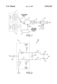
- FIG. 1 is a partial operational diagram of a radiotelephone according to the invention.
- FIG. 2 is a partial operational diagram of a transforming circuit included in a radiotelephone according to a preferred embodiment of the invention.
- FIG. 1 partially represents a radiotelephone according to the invention, arranged for transmitting or receiving signals in a first or a second frequency band.
- the first frequency band corresponds to that of the signals according to the GSM standard, whose nominal carrier frequency F1 is of the order of 950 MHz
- the second frequency band corresponds to that of the signals according to the DECT standard, whose nominal carrier frequency F2 is of the order of 1880 MHz.
- the radiotelephone comprises a first antenna-cum-filter system (1) intended to ensure the transmission or reception of signals in the first frequency band, a second antenna-cum-filter system (2) intended to transmit or receive signals in the second frequency band, and a selection device (3) for selecting the frequency band used and a frequency management device (4) controlling said selection device (3).
- a frequency conversion from either frequency band to an intermediate frequency FI is effected by the radiotelephone via a single local oscillator (7) which applies to a mixer (8) a signal VCO whose frequency FLO is a center frequency between the frequencies F1 and F2 of these two frequency bands.
- the mixer (8) may advantageously comprise a device which permits of the rejection of the image frequency and the compensation for linearity faults of the low-noise amplifier (6).
- the telephone further comprises a transforming circuit (5) which has an asymmetrical input terminal and two output terminals which form a symmetrical output, receiving on its asymmetrical input an asymmetrical signal Va produced by one of the antenna-cum-filter systems (1 or 2) and producing on its symmetrical output a symmetrical output signal Vs which is to be applied to the inputs of a single low-noise amplifier (6).
- the transforming circuit (5) comprises a symmetrizing circuit (9) which has an asymmetrical input and a symmetrical output, which can be tuned by a voltage called tuning control voltage Vtun produced by the frequency management device (4) to one or the other of the two frequency bands.
- the transforming circuit (5) further includes impedance adapting means between the symmetrical output of the symmetrizing circuit (9) and the input of the low-noise amplifier (6).
- the oscillator (7) and the mixer (8) effect, on the basis of the frequency FL0, a change by a lower value from the highest transmission/receiving frequency F2, and by a higher value from the lowest transmission/receiving frequency F1.
- FIG. 2 partially represents a transforming circuit (5) included in a radiotelephone according to a preferred embodiment of the invention.
- a transforming circuit (5) comprises a symmetrizing circuit (9) of the two T-cell type arranged in parallel, whose inputs are combined and thus form the asymmetrical input of the symmetrizing circuit (9).
- Each cell is formed by a phase shifting inductance L and a phase shifting capacitor C, the node between these elements forming the output of each cell.
- the outputs of the two cells form the symmetrical output of the symmetrizer.
- phase shifting inductances and capacitors L and C are arranged as a high-pass filter in one of the cells and a low-pass filter in the other, the phase shifting capacitors C being variable capacitance diodes which are subjected to the tuning control voltage Vtun.
- This transforming circuit (5) further comprises impedance adapting means which comprise:
- the transforming circuit (5) comprises two link capacitors Cl arranged in series between the series adaptation inductances Ls and the output terminals which form the symmetrical output of the transforming circuit (5).
- the values of the phase shifting inductances are kept constant in order to simplify the embodiment.
- the capacitors C thus are to be capable of adopting two values, C1 and C2, which respectively correspond to the tuning of the symmetrizing circuit (9) to the frequency F1 or F2. These values are then to satisfy the two relationships:
- the ratio F2/F1 being of the order of 2
- the ratio C1/C2 will thus be of the order of 4.
- a choice of values can be, for a same value L, for example, of the order of 12 nH, C1 of the order of 2.5 pF and C2 of the order of 0.6 pF.
- the output impedance of the symmetrizing circuit (9) will thus vary depending on whether it will be tuned to the first or the second frequency band, the phase shifting capacitors C adopting different values.
- the input impedance of the low-noise amplifier (6) also adopts different values depending on whether it operates in the first or second frequency band.
- the impedance adaptation elements Ls, Cp and Cs adapt the impedance seen on the output of the symmetrizing circuit (9) to the input impedance of the low-noise amplifier (6).
- the structure of the impedance adapting means is noteworthy because it effects, via fixed-value elements, an optimum adaptation of the impedances in their real components and a compensation for the reactive components in the two frequency bands used.
- the elements Ls, Cp and Cs could be determined precisely by means of a computer program in which the characteristic features of the input impedance of the low-noise amplifier (6) will be introduced. Such a computer program will, for example, produce the following values:
- link capacitances Cl The sole function of link capacitances Cl is to eliminate the DC components from the signals travelling between the transforming circuit (5) and the low-noise amplifier (6) which components could alter the polarization of the low-noise amplifier (6) and thus be harmful to the operation of the telephone, as, for example, the DC component of the output signal Vs which comes from the tuning control voltage Vtun.
- Values of the order of 10 pF will be selected for the decoupling capacitances, so that they do not have any significant influence on the tuning of the symmetrizing circuit (9) nor on the impedance adaptation between this symmetrizing circuit and the low-noise amplifier (6).
Abstract
Description
Claims (4)
Applications Claiming Priority (2)
| Application Number | Priority Date | Filing Date | Title |
|---|---|---|---|
| FR9602150 | 1996-02-21 | ||
| FR9602150A FR2745131A1 (en) | 1996-02-21 | 1996-02-21 | MULTIMODE RADIO TELEPHONY APPARATUS |
Publications (1)
| Publication Number | Publication Date |
|---|---|
| US5915223A true US5915223A (en) | 1999-06-22 |
Family
ID=9489442
Family Applications (1)
| Application Number | Title | Priority Date | Filing Date |
|---|---|---|---|
| US08/801,227 Expired - Lifetime US5915223A (en) | 1996-02-21 | 1997-02-19 | Multimode radiotelephone |
Country Status (5)
| Country | Link |
|---|---|
| US (1) | US5915223A (en) |
| EP (1) | EP0792027B1 (en) |
| JP (1) | JP3877825B2 (en) |
| DE (1) | DE69728599T2 (en) |
| FR (1) | FR2745131A1 (en) |
Cited By (9)
| Publication number | Priority date | Publication date | Assignee | Title |
|---|---|---|---|---|
| US6134452A (en) * | 1998-11-23 | 2000-10-17 | Motorola, Inc. | Multiple band mixer with common local oscillator |
| US6134427A (en) * | 1998-09-30 | 2000-10-17 | Conexant Systems, Inc. | Using a single low-noise amplifier in a multi-band wireless station |
| US6216012B1 (en) * | 1997-11-07 | 2001-04-10 | Conexant Systems, Inc. | Dualband power amplifier control using a single power amplifier controller |
| US6233463B1 (en) * | 1996-09-04 | 2001-05-15 | Globalstar L.P. | Automatic satellite terrestrial mobile terminal roaming system and method |
| US20030078037A1 (en) * | 2001-08-17 | 2003-04-24 | Auckland David T. | Methodology for portable wireless devices allowing autonomous roaming across multiple cellular air interface standards and frequencies |
| EP1455459A1 (en) * | 2003-03-05 | 2004-09-08 | Nec Corporation | Multi-band radio terminal and band switching method used thereof and program thereof |
| US20050143031A1 (en) * | 2002-02-06 | 2005-06-30 | Oswald Moonen | Multi-band receiver |
| US20100144285A1 (en) * | 2008-12-04 | 2010-06-10 | Broadcom Corporation | Extended antenna module and applications thereof |
| GB2500265A (en) * | 2012-03-16 | 2013-09-18 | Renesas Mobile Corp | Reconfigurable RF circuit using two filters arranged to pass different carrier frequencies connected to a single amplifier with a selectable frequency range |
Families Citing this family (1)
| Publication number | Priority date | Publication date | Assignee | Title |
|---|---|---|---|---|
| DK0932251T3 (en) | 1998-01-23 | 2005-05-23 | Siemens Ag | Radio transmitter and radio receiver |
Citations (16)
| Publication number | Priority date | Publication date | Assignee | Title |
|---|---|---|---|---|
| US3054057A (en) * | 1960-07-13 | 1962-09-11 | Gen Dynamics Corp | Digitally tuned transmitter-receiver |
| US3639686A (en) * | 1969-04-25 | 1972-02-01 | Homarket Inc | Television receiver cut-in device |
| US3767112A (en) * | 1970-08-28 | 1973-10-23 | Matsushita Electric Ind Co Ltd | Frequency presetting equipment |
| US4115737A (en) * | 1975-11-13 | 1978-09-19 | Sony Corporation | Multi-band tuner |
| US4132952A (en) * | 1975-11-11 | 1979-01-02 | Sony Corporation | Multi-band tuner with fixed broadband input filters |
| US4167703A (en) * | 1977-05-17 | 1979-09-11 | Sony Corporation | Tuning apparatus with band-selection means |
| US4234965A (en) * | 1978-06-28 | 1980-11-18 | Motorola, Inc. | Communication tuning system utilizing local oscillator frequency selection for maximum RF filter bandwidth and method thereof |
| US4408347A (en) * | 1977-07-29 | 1983-10-04 | Texas Instruments Incorporated | High-frequency channel selector having fixed bandpass filters in the RF section |
| US5249302A (en) * | 1987-10-09 | 1993-09-28 | Motorola, Inc. | Mixed-mode transceiver system |
| US5280636A (en) * | 1991-06-13 | 1994-01-18 | Hughes Aircraft Company | Multi-band digital receiving apparatus and method with bandwidth reduction |
| EP0653851A2 (en) * | 1993-11-12 | 1995-05-17 | Philips Patentverwaltung GmbH | Multiband radio transceiver |
| US5477532A (en) * | 1992-10-22 | 1995-12-19 | Kokusai Electric Co. | Radio transceiver |
| US5530928A (en) * | 1994-01-31 | 1996-06-25 | Qualcomm Incorporated | Balanced dual mode mixer apparatus |
| US5548840A (en) * | 1992-02-03 | 1996-08-20 | Motorola, Inc. | Balanced mixer circuit with improved linearity |
| US5564098A (en) * | 1994-09-13 | 1996-10-08 | Trimble Navigation Limited | Ultra low-power integrated circuit for pseudo-baseband down-conversion of GPS RF signals |
| US5630213A (en) * | 1992-12-22 | 1997-05-13 | Motorola, Inc. | RF antenna switch and method of operating the same |
Family Cites Families (5)
| Publication number | Priority date | Publication date | Assignee | Title |
|---|---|---|---|---|
| FR917372A (en) * | 1944-12-08 | 1947-01-06 | Patelhold Patentverwertung | Impedance matching system from an asymmetric circuit to a symmetrical circuit, or vice versa |
| KR870001910B1 (en) * | 1985-05-31 | 1987-10-21 | 삼성전자부품 주식회사 | High/low pass filter |
| FR2685586A1 (en) * | 1991-12-19 | 1993-06-25 | Sagem | Device for routing in terms of frequency, with impedance matching |
| GB2278253B (en) * | 1993-05-05 | 1996-08-28 | Marconi Gec Ltd | An integrated transceiver circuit packaged component |
| JP2586333B2 (en) * | 1994-05-13 | 1997-02-26 | 日本電気株式会社 | Wireless communication device |
-
1996
- 1996-02-21 FR FR9602150A patent/FR2745131A1/en not_active Withdrawn
-
1997
- 1997-02-13 EP EP97200400A patent/EP0792027B1/en not_active Expired - Lifetime
- 1997-02-13 DE DE69728599T patent/DE69728599T2/en not_active Expired - Lifetime
- 1997-02-19 JP JP03505497A patent/JP3877825B2/en not_active Expired - Lifetime
- 1997-02-19 US US08/801,227 patent/US5915223A/en not_active Expired - Lifetime
Patent Citations (16)
| Publication number | Priority date | Publication date | Assignee | Title |
|---|---|---|---|---|
| US3054057A (en) * | 1960-07-13 | 1962-09-11 | Gen Dynamics Corp | Digitally tuned transmitter-receiver |
| US3639686A (en) * | 1969-04-25 | 1972-02-01 | Homarket Inc | Television receiver cut-in device |
| US3767112A (en) * | 1970-08-28 | 1973-10-23 | Matsushita Electric Ind Co Ltd | Frequency presetting equipment |
| US4132952A (en) * | 1975-11-11 | 1979-01-02 | Sony Corporation | Multi-band tuner with fixed broadband input filters |
| US4115737A (en) * | 1975-11-13 | 1978-09-19 | Sony Corporation | Multi-band tuner |
| US4167703A (en) * | 1977-05-17 | 1979-09-11 | Sony Corporation | Tuning apparatus with band-selection means |
| US4408347A (en) * | 1977-07-29 | 1983-10-04 | Texas Instruments Incorporated | High-frequency channel selector having fixed bandpass filters in the RF section |
| US4234965A (en) * | 1978-06-28 | 1980-11-18 | Motorola, Inc. | Communication tuning system utilizing local oscillator frequency selection for maximum RF filter bandwidth and method thereof |
| US5249302A (en) * | 1987-10-09 | 1993-09-28 | Motorola, Inc. | Mixed-mode transceiver system |
| US5280636A (en) * | 1991-06-13 | 1994-01-18 | Hughes Aircraft Company | Multi-band digital receiving apparatus and method with bandwidth reduction |
| US5548840A (en) * | 1992-02-03 | 1996-08-20 | Motorola, Inc. | Balanced mixer circuit with improved linearity |
| US5477532A (en) * | 1992-10-22 | 1995-12-19 | Kokusai Electric Co. | Radio transceiver |
| US5630213A (en) * | 1992-12-22 | 1997-05-13 | Motorola, Inc. | RF antenna switch and method of operating the same |
| EP0653851A2 (en) * | 1993-11-12 | 1995-05-17 | Philips Patentverwaltung GmbH | Multiband radio transceiver |
| US5530928A (en) * | 1994-01-31 | 1996-06-25 | Qualcomm Incorporated | Balanced dual mode mixer apparatus |
| US5564098A (en) * | 1994-09-13 | 1996-10-08 | Trimble Navigation Limited | Ultra low-power integrated circuit for pseudo-baseband down-conversion of GPS RF signals |
Cited By (15)
| Publication number | Priority date | Publication date | Assignee | Title |
|---|---|---|---|---|
| US6233463B1 (en) * | 1996-09-04 | 2001-05-15 | Globalstar L.P. | Automatic satellite terrestrial mobile terminal roaming system and method |
| US6216012B1 (en) * | 1997-11-07 | 2001-04-10 | Conexant Systems, Inc. | Dualband power amplifier control using a single power amplifier controller |
| US6134427A (en) * | 1998-09-30 | 2000-10-17 | Conexant Systems, Inc. | Using a single low-noise amplifier in a multi-band wireless station |
| US6134452A (en) * | 1998-11-23 | 2000-10-17 | Motorola, Inc. | Multiple band mixer with common local oscillator |
| US20030078037A1 (en) * | 2001-08-17 | 2003-04-24 | Auckland David T. | Methodology for portable wireless devices allowing autonomous roaming across multiple cellular air interface standards and frequencies |
| US20050143031A1 (en) * | 2002-02-06 | 2005-06-30 | Oswald Moonen | Multi-band receiver |
| US20040204039A1 (en) * | 2003-03-05 | 2004-10-14 | Nec Corporation | Multi-bank radio terminal and band switching method used therefor and program thereof |
| EP1455459A1 (en) * | 2003-03-05 | 2004-09-08 | Nec Corporation | Multi-band radio terminal and band switching method used thereof and program thereof |
| US7085586B2 (en) | 2003-03-05 | 2006-08-01 | Nec Corporation | Multi-band radio terminal and band switching method used therefor and program thereof |
| US20100144285A1 (en) * | 2008-12-04 | 2010-06-10 | Broadcom Corporation | Extended antenna module and applications thereof |
| US8270925B2 (en) * | 2008-12-04 | 2012-09-18 | Broadcom Corporation | Extended antenna module and applications thereof |
| GB2500265A (en) * | 2012-03-16 | 2013-09-18 | Renesas Mobile Corp | Reconfigurable RF circuit using two filters arranged to pass different carrier frequencies connected to a single amplifier with a selectable frequency range |
| US20130244722A1 (en) * | 2012-03-16 | 2013-09-19 | Renesas Mobile Corporation | Reconfigurable radio frequency circuits and methods of receiving |
| GB2500265B (en) * | 2012-03-16 | 2014-03-05 | Broadcom Corp | Reconfigurable radio frequency circuits and methods of receiving |
| US9154171B2 (en) * | 2012-03-16 | 2015-10-06 | Broadcom Corporation | Reconfigurable radio frequency circuits and methods of receiving |
Also Published As
| Publication number | Publication date |
|---|---|
| EP0792027B1 (en) | 2004-04-14 |
| EP0792027A1 (en) | 1997-08-27 |
| FR2745131A1 (en) | 1997-08-22 |
| DE69728599D1 (en) | 2004-05-19 |
| JPH104372A (en) | 1998-01-06 |
| JP3877825B2 (en) | 2007-02-07 |
| DE69728599T2 (en) | 2005-04-14 |
Similar Documents
| Publication | Publication Date | Title |
|---|---|---|
| US7095454B2 (en) | Broadband single conversion tuner integrated circuits | |
| US5216392A (en) | Automatically controlled varactor tuned matching networks for a crystal filter | |
| US6366166B1 (en) | Double pass band amplifier circuit and a radio frequency reception head | |
| US7251466B2 (en) | Television receiver including an integrated band selection filter | |
| US20050040909A1 (en) | Broadband integrated digitally tunable filters | |
| US5451915A (en) | Active filter resonator and system and negative resistance generator usable therein | |
| US6882223B2 (en) | Multi-band low noise amplifier | |
| US5392011A (en) | Tunable filter having capacitively coupled tuning elements | |
| US20020067211A1 (en) | Power amplifier | |
| JPH09232915A (en) | Radio frequency filter device provided with image trap | |
| EP0823145A1 (en) | Tunable interstage filter | |
| US9851384B2 (en) | Multi-band impedance detector | |
| US5915223A (en) | Multimode radiotelephone | |
| KR100260965B1 (en) | Amplifier and portable telephone apparatus using the same | |
| US7106149B2 (en) | Switchable tuneable bandpass filter with optimized frequency response | |
| US4569085A (en) | Oscillator control circuit in an F.M. receiver | |
| EP1236285B1 (en) | Receiver circuit | |
| US5499056A (en) | Bandswitchable double tuned RF circuit with balanced secondary | |
| MXPA05000704A (en) | Wideband vco resonant circuit method and apparatus. | |
| US5619283A (en) | Double tuned RF circuit with balanced secondary | |
| US6754478B1 (en) | CMOS low noise amplifier | |
| US5574413A (en) | Tunable filter having a capacitive circuit connected to ground | |
| US6441701B1 (en) | Tunable bridged-T filter | |
| US6177832B1 (en) | High frequency differential to single-ended converter | |
| US6545554B1 (en) | Differential oscillator |
Legal Events
| Date | Code | Title | Description |
|---|---|---|---|
| AS | Assignment |
Owner name: U.S. PHILIPS CORPORATION, NEW YORK Free format text: ASSIGNMENT OF ASSIGNORS INTEREST;ASSIGNORS:LECUYER, MATHIEU;LOGOGUEZ, BRUNO;REEL/FRAME:008547/0399 Effective date: 19970414 |
|
| STCF | Information on status: patent grant |
Free format text: PATENTED CASE |
|
| FPAY | Fee payment |
Year of fee payment: 4 |
|
| FPAY | Fee payment |
Year of fee payment: 8 |
|
| AS | Assignment |
Owner name: NXP B.V., NETHERLANDS Free format text: ASSIGNMENT OF ASSIGNORS INTEREST;ASSIGNOR:U.S. PHILIPS CORPORATION;REEL/FRAME:018635/0755 Effective date: 20061127 |
|
| AS | Assignment |
Owner name: MORGAN STANLEY SENIOR FUNDING, INC., ENGLAND Free format text: SECURITY AGREEMENT;ASSIGNOR:NXP B.V.;REEL/FRAME:018806/0201 Effective date: 20061201 |
|
| AS | Assignment |
Owner name: NXP, B.V., NETHERLANDS Free format text: RELEASE BY SECURED PARTY;ASSIGNOR:MORGAN STANLEY SENIOR FUNDING, INC.;REEL/FRAME:021478/0653 Effective date: 20080902 |
|
| FPAY | Fee payment |
Year of fee payment: 12 |
|
| AS | Assignment |
Owner name: ST WIRELESS SA, SWITZERLAND Free format text: ASSIGNMENT OF ASSIGNORS INTEREST;ASSIGNOR:NXP B.V.;REEL/FRAME:037624/0831 Effective date: 20080728 |
|
| AS | Assignment |
Owner name: ST-ERICSSON SA, SWITZERLAND Free format text: CHANGE OF NAME;ASSIGNOR:ST WIRELESS SA;REEL/FRAME:037683/0128 Effective date: 20080714 Owner name: ST-ERICSSON SA, EN LIQUIDATION, SWITZERLAND Free format text: STATUS CHANGE-ENTITY IN LIQUIDATION;ASSIGNOR:ST-ERICSSON SA;REEL/FRAME:037739/0493 Effective date: 20150223 |
|
| AS | Assignment |
Owner name: NXP B.V., NETHERLANDS Free format text: RELEASE BY SECURED PARTY;ASSIGNOR:MORGAN STANLEY SENIOR FUNDING, INC;REEL/FRAME:050315/0443 Effective date: 20190903 |