US5920514A - Memory device with efficient redundancy using sense amplifiers - Google Patents
Memory device with efficient redundancy using sense amplifiers Download PDFInfo
- Publication number
- US5920514A US5920514A US08/918,508 US91850897A US5920514A US 5920514 A US5920514 A US 5920514A US 91850897 A US91850897 A US 91850897A US 5920514 A US5920514 A US 5920514A
- Authority
- US
- United States
- Prior art keywords
- sense amplifier
- circuit
- amplifier circuit
- output
- pair
- Prior art date
- Legal status (The legal status is an assumption and is not a legal conclusion. Google has not performed a legal analysis and makes no representation as to the accuracy of the status listed.)
- Expired - Lifetime
Links
Images


Classifications
-
- G—PHYSICS
- G11—INFORMATION STORAGE
- G11C—STATIC STORES
- G11C29/00—Checking stores for correct operation ; Subsequent repair; Testing stores during standby or offline operation
- G11C29/70—Masking faults in memories by using spares or by reconfiguring
- G11C29/78—Masking faults in memories by using spares or by reconfiguring using programmable devices
- G11C29/84—Masking faults in memories by using spares or by reconfiguring using programmable devices with improved access time or stability
- G11C29/848—Masking faults in memories by using spares or by reconfiguring using programmable devices with improved access time or stability by adjacent switching
-
- G—PHYSICS
- G11—INFORMATION STORAGE
- G11C—STATIC STORES
- G11C11/00—Digital stores characterised by the use of particular electric or magnetic storage elements; Storage elements therefor
- G11C11/21—Digital stores characterised by the use of particular electric or magnetic storage elements; Storage elements therefor using electric elements
- G11C11/34—Digital stores characterised by the use of particular electric or magnetic storage elements; Storage elements therefor using electric elements using semiconductor devices
- G11C11/40—Digital stores characterised by the use of particular electric or magnetic storage elements; Storage elements therefor using electric elements using semiconductor devices using transistors
- G11C11/401—Digital stores characterised by the use of particular electric or magnetic storage elements; Storage elements therefor using electric elements using semiconductor devices using transistors forming cells needing refreshing or charge regeneration, i.e. dynamic cells
- G11C11/4063—Auxiliary circuits, e.g. for addressing, decoding, driving, writing, sensing or timing
- G11C11/407—Auxiliary circuits, e.g. for addressing, decoding, driving, writing, sensing or timing for memory cells of the field-effect type
- G11C11/409—Read-write [R-W] circuits
- G11C11/4091—Sense or sense/refresh amplifiers, or associated sense circuitry, e.g. for coupled bit-line precharging, equalising or isolating
-
- G—PHYSICS
- G11—INFORMATION STORAGE
- G11C—STATIC STORES
- G11C7/00—Arrangements for writing information into, or reading information out from, a digital store
- G11C7/06—Sense amplifiers; Associated circuits, e.g. timing or triggering circuits
-
- G—PHYSICS
- G11—INFORMATION STORAGE
- G11C—STATIC STORES
- G11C7/00—Arrangements for writing information into, or reading information out from, a digital store
- G11C7/10—Input/output [I/O] data interface arrangements, e.g. I/O data control circuits, I/O data buffers
Definitions
- the present invention relates generally to memory devices and in particular the present invention relates to redundant circuitry in a memory device.
- An integrated circuit is a complete electronic circuit, containing transistors, diodes, resistors, and capacitors, along with their interconnecting electrical conductors, contained entirely within a single chip of silicon. Integrated circuits continue to decrease in size, and the circuits they contain continue to increase in complexity. This increases the chances of defective chips resulting from a failed element or a defective conductor.
- a redundant element can be substituted for that defective element.
- An integrated circuit device which uses redundant elements is electronic memory.
- Typical memory circuits comprise millions of equivalent memory cells arranged in addressable rows and columns. By providing redundant elements, defective memory cells or columns can be replaced. Because the individual primary memory cells of a memory are separately addressable, replacing a defective cell typically comprises opening fuse-type circuits to ⁇ program ⁇ a redundant cell to respond to the address of the defective primary cell. This process is very effective for permanently replacing defective primary memory cells. For example, FIG.
- FIG. 1 illustrates a typical memory circuit where primary memory columns (PRIME 0 to PRIME i ) are selectively connected to data communication lines (DATA 0 and DATA i ).
- primary memory columns PRIME 0 to PRIME i
- DATA 0 and DATA i data communication lines
- the appropriate select signal SEL 0 to SEL i
- a primary column is determined to be defective, its select signal is forced to a permanent inactive state, and a compare circuit is programmed to activate an appropriate redundant select signal (RSEL 0 to RSEL i ). This programming is typically performed using fusible circuits.
- the compare circuit responds by activating the redundant select signal to couple the redundant column to the appropriate data communication line.
- a memory which has memory storage cells coupled to data bit lines.
- Sense amplifier circuits are provided to receive input from the data bit lines and produce an output in response thereto.
- the memory includes circuitry which shifts the input to the sense amplifiers. Thus, input data bit lines for a first sense amplifier are shifted to a second sense amplifier such that redundant memory storage cells and data bit lines can be substituted for defective ones.
- the present invention describes a memory device comprising memory storage cells for storing data, data communication lines coupled to the memory storage cells, sense amplifier circuits having multiple inputs coupled to the data communication lines.
- the plurality of sense amplifier circuits each having an output.
- the memory further comprises select circuitry connected to the sense amplifier circuits to couple one of the multiple inputs of each of the sense amplifier circuits to the output of the sense amplifier circuits.
- a memory device which comprises memory cells, a first pair of data communication bit lines, and a second pair of data communication bit lines.
- the memory also comprises addressing circuitry for selectively coupling the memory cells to the first and second pair of data communication bit lines, a first sense amplifier circuit coupled to the first and second pair of data communication bit lines for producing an output in response to the first pair of data communication bit lines, and select circuitry connected to the first sense amplifier circuit for enabling the first sense amplifier circuit to produce the output in response the second pair of data communication bit lines.
- a method of providing redundancy in a memory device comprises the steps of disabling a sense amplifier circuit associated with a first plurality of memory cells from producing an output in response to the first plurality of memory cells, and enabling the sense amplifier circuit associated with the first plurality of memory cells to produce the output in response to a plurality of redundant memory cells.
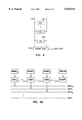
- FIG. 1 is a block diagram of a portion of a prior art memory device
- FIG. 2 is a schematic diagram of a portion of a dynamic random access memory (DRAM);
- DRAM dynamic random access memory
- FIG. 3 is a block diagram of a static random access memory (SRAM).
- SRAM static random access memory
- FIG. 4 illustrates one column of a typical SRAM of FIG. 3
- FIG. 5a is a block diagram of the read circuitry of present invention.
- FIG. 5b is a block diagram of the write circuitry of present invention.
- FIG. 6 is a block diagram of an SRAM incorporating the present invention.
- FIG. 7 is a schematic diagram of one embodiment of sense amplifier and select circuitry of FIG. 6.
- a memory circuit comprises memory cells which store data. Depending upon the type of memory, this data can be read, or read and written. That is, some memories are read-only while others allow data to be read, manipulated, and re-written. Because many types of dynamic memories store data as a charge on a capacitor, sense amplifiers are implemented to detect small charges and amplify the charge for further processing. Static memories utilize sense amplifier circuits to detect data stored in memory cells.
- Dynamic random access memories typically use memory cells fabricated as capacitors. These cells can be selectively connected to digit lines 104 which are connected to a sense amplifier, as shown in FIG. 2.
- the memory cells 108 are each connected to the source of an access transistor 110.
- the drain of the transistor is connected to a digit line 104, or column of memory cells.
- the gate of the transistor is connected to a word line 112, or memory row, which is used to selectively connect one of the memory cells to the digit lines.
- the sense amplifier 100 is typically comprised of two amplifiers; an n-sense amp 114 and a p-sense amp 116. Isolation transistors 118 are provided between the digit lines 104 and the sense amplifiers 114 and 116.
- the digit lines 104 are pre-charged to Vcc/2 and then an access transistor 110 connected to a memory cell is selectively activated by providing a high voltage on its associated word line 112. The memory cell is then electrically connected to the digit line 104 through the access transistor. Any charge stored on the memory cell capacitor is shared with the digit line. The potential of the digit line will typically only change by a fraction of a volt, approximately 200 mv.
- the n-sense amplifier is activated to connect one of the digit lines 104 to a low voltage. If the selected memory cell 108 has data stored as a high voltage, the complementary digit line connected to the sense amplifiers will be forced low by the n-sense amp 116. Similarly, if the selected memory cell has data stored as a discharged capacitor the coupled digit line is forced low by the n-sense amp.
- the p-sense amp 116 is activated.
- the compliment to the digit line, therefore, which was pulled low by the n-sense amp will be forced high using the p-sense amplifier. If the selected memory cell has data stored as a voltage, the coupled digit line will be forced high by the p-sense amp. Thus, by using both sense amplifiers the digit line associated with the memory cell has been forced to a power rail representing the data stored on the memory cell.
- Static random access memories are similar to the above described DRAMs. Data is stored in memory cells which are selectively accessed through externally provided addresses.
- the typical static memory cell is a latch circuit which is more complicated than the typical dynamic memory cell, thereby reducing the available memory density of SRAMs. SRAMs, however, can be operated at faster data rates and are ideal for applications such as cache memories.
- the SRAM includes a memory array 132 of static memory cells.
- Address decode circuitry 134 is provided to decode an address provided on the address inputs and access the memory array.
- Control circuitry 136 controls the read and write operations performed by the memory in response to external control inputs. Data read from the memory array is sensed and amplified by sense amplifier circuit 138 and output on data communication lines (DQ) via output buffer 140. Data provided on the DQ lines is written to the memory array through input buffer/driver circuit 142.
- DQ data communication lines
- Memory array 132 is arranged in rows and columns of memory cells.
- the columns are defined by a pair of bit lines which communicate data stored in the memory cells to the sense amplifier circuits.
- the bit lines are complements of each other such that in an active state one bit line will be at a low signal level and the other bit line will be at a high signal level.
- FIG. 4 illustrates one column of a typical SRAM.
- the memory cells 144 are selectively connected to one of a pair of bit lines 146 in response to address decode circuitry 134.
- Equilibrate circuit 148 is provided to equalize the bit line pair to a pre-determined voltage prior to reading data from the memory cells, as known to those skilled in the art.
- the equilibrated bit line voltage When a memory cell is coupled to a bit line, the equilibrated bit line voltage will be adjusted to reflect the data stored in the selected memory cell. For example, if the bit line where pre-charged to a high voltage and the data stored on a selected memory cell is represented by a low voltage, the bit line voltage will be reduced to a low voltage.
- Sense amplifier circuity 150 is a subset of sense amplifier 138 and typically comprises a two-stage circuit. One of the stages senses the bit line which has a higher voltage and amplifies that bit line voltage to a higher level. The other stage senses the bit line with the lower voltage and amplifies that voltage to a lower voltage level. The amplified bit line voltages are then provided to a buffer circuit for communication to the DQ lines.
- DRAM and SRAM include circuitry not described in detail herein.
- the description of these memories is intended to provide a basic understanding of memories so that the features and advantages of the present invention can be fully understood.
- the present invention is described in detail as being incorporated in an SRAM, but can be equally incorporated in any memory circuit using sense amplifier circuitry, such as DRAMs.
- the read circuitry of the present invention can be implemented in any integrated circuit, including but not limited to SRAMs and DRAMs, to provide a redundancy scheme where a defective primary column of memory cells can be replaced with a redundant column.
- the present invention eliminates the need for either primary column disabling circuitry or redundant column compare and select circuitry, as described above in the background.
- the redundant scheme provides a memory device in which the sense amplifier circuits associated with the memory columns can be enabled to accept input from its nearest neighboring column. Switching circuitry is provided which allows the sense amplifier of a defective column to bypass the defective column and multiplex the redundant column. As illustrated in FIG. 5, sense amplifier SAMP 1 accepts input from column PRIME 2 and data is output on DATA 1 while SAMP 2 accepts input from redundant column REDUN and data is output on DATA 2 .
- the switching circuitry is programmed to route input data to the appropriate column in accordance with the sense amplifier routing discussed with reference to FIG. 5a.
- the write circuitry includes switches labeled Switch0 to Switch2 which route input data from communication lines DATA0 to DATA1 to the memory columns.
- DATA0 is routed to PRIME0
- DATA1 is routed to PRIME2
- DATA2 is routed to REDUN. It will be appreciated by those skilled in the art that any switching circuitry can be implemented to insure that bidirectional communication is maintained with the columns.
- FIG. 6 illustrates two pairs of bit lines A and B each having an associated first sense amplifier stage 160.
- the first stage couples the bit lines to intermediate bit line pairs A' and B'.
- Sense amplifier select circuitry 162(a) and (b) are provided to couple one pair of intermediate bit lines to the second stage sense amplifier circuit 164(a) and (b).
- Intermediate bit lines A' or intermediate bit lines B' will, therefore, be coupled to sense amplifier 164(b).
- intermediate bit lines B' can either be coupled to the next sense amplifier circuit 164(c) (not shown) using its sense amplifier select circuitry 162(c) (not shown), or not coupled to sense amplifier 164(c) if bit line pair B or memory cells coupled thereto are defective.
- the redundant column can be coupled to sense amplifier 164(a) through sense amplifier select circuit 162(a) for output on DATA(a).
- FIG. 7 is a detailed schematic of one pair of bit lines A and A*, select circuit, sense amplifier select circuit and two stage sense amplifier.
- Bit lines A and A* are connected to equilibration circuit 180 to pre-charge the bit lines to a high voltage prior to reading a memory cell.
- First stage sense amplifier 182 receives bit lines A and A*.
- block select signal (BSEL) is high, transistor 184 is activated which activates transistors 186 and 188.
- the drains of transistors 190 and 192 and intermediate bit lines A' and A'* and are coupled low through transistors 194 and 196, respectively, when the bit lines A and A* are high.
- transistor 190 or 192 is turned off and the corresponding intermediate bit line is pulled high through either transistor 186 or 188.
- the second stage of the sense amplifier circuit is illustrated in two halves 198 and 200.
- Sense amplifier half 198 provides output 206, while half 200 provides output 208.
- Each half of the second stage sense amplifier is coupled to either intermediate bit line pairs A' and A'* or the intermediate bit line pair of the neighboring column, RED' and RED'*.
- the neighboring column in this illustration is a redundant column, but can be any neighboring column and not limited to redundant circuits.
- Select circuits 202 and 204 are connected to sense amplifier halves 198 and 200, respectively, and are used to enable the sense amplifier halves.
- Each select circuit comprises pull-down transistors 210(a) and 210(b) which are activated in response to a select signal (SEL).
- the SEL is preferably an internal signal provided by a redundancy enable circuit such as a fuseable link, as known to those skilled in the art. Either transistor 210(a) or 210(b) will be activated by the SEL signal to couple the appropriate intermediate bit line pair to the second stage sense amplifier circuit.
- the second stage sense amplifier halves include current mirror circuits comprised of transistors 212 and 214.
- the sources of transistors 212 and 214 are connected to transistors 216(a)-(b) and 218(a)-(b), respectively.
- Transistors 216(a)-(b) and 218(a)-(b) are also coupled to pull-down transistors 210(a) or 210(b).
- the select signal SEL By controlling the select signal SEL, the intermediate bit line pair which is to be coupled to outputs 206 and 208 can be selected. That is, when SEL is high transistor 210(b) is activated and transistors 216(b) and 218(b) respond to intermediate bit lines A' and A'*.
- transistors 216(a) and 218(a) respond to intermediate bit lines RED' and RED'*.
- the current mirror circuit of each half of the second sense amplifier stage in combination with either transistors 216(a) and 218(a) or 216(b) and 218(b) produce a differential output on line 206 and 208.
- Outputs 206 and 208 are connected to buffer/driver circuitry for output on the DQ lines.
- a memory device has been described which has memory storage cells coupled to data bit lines.
- Sense amplifier circuits are provided to receive input from the data bit lines and produce an output in response thereto.
- the memory includes redundant circuitry which shifts the input to the sense amplifiers. Data bit lines from a neighboring sense amplifier are shifted to another sense amplifier such that redundant memory storage cells and data bit lines can be substituted for defective ones.
- the redundant circuitry can be used on any type of memory circuit having memory cells coupled to data communication lines, including but not limited to DRAM, SDRAM, SRAM and VRAM's.
Abstract
Description
Claims (23)
Priority Applications (1)
| Application Number | Priority Date | Filing Date | Title |
|---|---|---|---|
| US08/918,508 US5920514A (en) | 1996-11-15 | 1997-08-22 | Memory device with efficient redundancy using sense amplifiers |
Applications Claiming Priority (2)
| Application Number | Priority Date | Filing Date | Title |
|---|---|---|---|
| US08/751,002 US5694368A (en) | 1996-11-15 | 1996-11-15 | Memory device with efficient redundancy using sense amplifiers |
| US08/918,508 US5920514A (en) | 1996-11-15 | 1997-08-22 | Memory device with efficient redundancy using sense amplifiers |
Related Parent Applications (1)
| Application Number | Title | Priority Date | Filing Date |
|---|---|---|---|
| US08/751,002 Continuation US5694368A (en) | 1996-11-15 | 1996-11-15 | Memory device with efficient redundancy using sense amplifiers |
Publications (1)
| Publication Number | Publication Date |
|---|---|
| US5920514A true US5920514A (en) | 1999-07-06 |
Family
ID=25020039
Family Applications (2)
| Application Number | Title | Priority Date | Filing Date |
|---|---|---|---|
| US08/751,002 Expired - Lifetime US5694368A (en) | 1996-11-15 | 1996-11-15 | Memory device with efficient redundancy using sense amplifiers |
| US08/918,508 Expired - Lifetime US5920514A (en) | 1996-11-15 | 1997-08-22 | Memory device with efficient redundancy using sense amplifiers |
Family Applications Before (1)
| Application Number | Title | Priority Date | Filing Date |
|---|---|---|---|
| US08/751,002 Expired - Lifetime US5694368A (en) | 1996-11-15 | 1996-11-15 | Memory device with efficient redundancy using sense amplifiers |
Country Status (1)
| Country | Link |
|---|---|
| US (2) | US5694368A (en) |
Cited By (8)
| Publication number | Priority date | Publication date | Assignee | Title |
|---|---|---|---|---|
| US6373759B2 (en) | 2000-03-31 | 2002-04-16 | Matsushita Electric Industrial Co., Ltd. | SRAM device |
| US6445625B1 (en) | 2000-08-25 | 2002-09-03 | Micron Technology, Inc. | Memory device redundancy selection having test inputs |
| US6496425B1 (en) | 2000-08-21 | 2002-12-17 | Micron Technology, Inc | Multiple bit line column redundancy |
| US6504768B1 (en) | 2000-08-25 | 2003-01-07 | Micron Technology, Inc. | Redundancy selection in memory devices with concurrent read and write |
| US6525974B2 (en) * | 1998-12-22 | 2003-02-25 | Infineon Technologies Ag | Integrated memory with redundancy |
| US20050248998A1 (en) * | 2004-05-07 | 2005-11-10 | Jung Chul M | High speed redundant data sensing method and apparatus |
| US20080219072A1 (en) * | 2006-03-31 | 2008-09-11 | Kristopher Chad Breen | Method and apparatus for a dynamic semiconductor memory with compact sense amplifier circuit |
| US10134486B2 (en) | 2016-09-13 | 2018-11-20 | Samsung Electronics Co., Ltd. | Memory device including a redundancy column and a redundancy peripheral logic circuit |
Families Citing this family (3)
| Publication number | Priority date | Publication date | Assignee | Title |
|---|---|---|---|---|
| US6522592B2 (en) | 2001-04-19 | 2003-02-18 | Micron Technology, Inc. | Sense amplifier for reduction of access device leakage |
| US7372092B2 (en) * | 2005-05-05 | 2008-05-13 | Micron Technology, Inc. | Memory cell, device, and system |
| US20080291760A1 (en) * | 2007-05-23 | 2008-11-27 | Micron Technology, Inc. | Sub-array architecture memory devices and related systems and methods |
Citations (11)
| Publication number | Priority date | Publication date | Assignee | Title |
|---|---|---|---|---|
| US4937465A (en) * | 1988-12-08 | 1990-06-26 | Micron Technology, Inc. | Semiconductor fuse blowing and verifying method and apparatus |
| US5110754A (en) * | 1991-10-04 | 1992-05-05 | Micron Technology, Inc. | Method of making a DRAM capacitor for use as an programmable antifuse for redundancy repair/options on a DRAM |
| US5212442A (en) * | 1992-03-20 | 1993-05-18 | Micron Technology, Inc. | Forced substrate test mode for packaged integrated circuits |
| US5280205A (en) * | 1992-04-16 | 1994-01-18 | Micron Technology, Inc. | Fast sense amplifier |
| US5279975A (en) * | 1992-02-07 | 1994-01-18 | Micron Technology, Inc. | Method of testing individual dies on semiconductor wafers prior to singulation |
| US5281868A (en) * | 1992-08-18 | 1994-01-25 | Micron Technology, Inc. | Memory redundancy addressing circuit for adjacent columns in a memory |
| US5392245A (en) * | 1993-08-13 | 1995-02-21 | Micron Technology, Inc. | Redundancy elements using thin film transistors (TFTs) |
| US5424672A (en) * | 1994-02-24 | 1995-06-13 | Micron Semiconductor, Inc. | Low current redundancy fuse assembly |
| US5528539A (en) * | 1994-09-29 | 1996-06-18 | Micron Semiconductor, Inc. | High speed global row redundancy system |
| US5574698A (en) * | 1993-12-13 | 1996-11-12 | Micron Technology, Inc. | Ram row decode circuitry that utilizes a precharge circuit that is deactivated by a feedback from an activated word line driver |
| US5583463A (en) * | 1995-05-30 | 1996-12-10 | Micron Technology, Inc. | Redundant row fuse bank circuit |
Family Cites Families (1)
| Publication number | Priority date | Publication date | Assignee | Title |
|---|---|---|---|---|
| US5371707A (en) * | 1992-01-30 | 1994-12-06 | Nec Corporation | Dynamic random access memory device equipped with dummy cells implemented by enhancement type transistors |
-
1996
- 1996-11-15 US US08/751,002 patent/US5694368A/en not_active Expired - Lifetime
-
1997
- 1997-08-22 US US08/918,508 patent/US5920514A/en not_active Expired - Lifetime
Patent Citations (13)
| Publication number | Priority date | Publication date | Assignee | Title |
|---|---|---|---|---|
| US4937465A (en) * | 1988-12-08 | 1990-06-26 | Micron Technology, Inc. | Semiconductor fuse blowing and verifying method and apparatus |
| US5110754A (en) * | 1991-10-04 | 1992-05-05 | Micron Technology, Inc. | Method of making a DRAM capacitor for use as an programmable antifuse for redundancy repair/options on a DRAM |
| US5391892A (en) * | 1992-02-07 | 1995-02-21 | Micron Technology, Inc. | Semiconductor wafers having test circuitry for individual dies |
| US5279975A (en) * | 1992-02-07 | 1994-01-18 | Micron Technology, Inc. | Method of testing individual dies on semiconductor wafers prior to singulation |
| US5212442A (en) * | 1992-03-20 | 1993-05-18 | Micron Technology, Inc. | Forced substrate test mode for packaged integrated circuits |
| US5280205A (en) * | 1992-04-16 | 1994-01-18 | Micron Technology, Inc. | Fast sense amplifier |
| US5281868A (en) * | 1992-08-18 | 1994-01-25 | Micron Technology, Inc. | Memory redundancy addressing circuit for adjacent columns in a memory |
| US5392245A (en) * | 1993-08-13 | 1995-02-21 | Micron Technology, Inc. | Redundancy elements using thin film transistors (TFTs) |
| US5574698A (en) * | 1993-12-13 | 1996-11-12 | Micron Technology, Inc. | Ram row decode circuitry that utilizes a precharge circuit that is deactivated by a feedback from an activated word line driver |
| US5424672A (en) * | 1994-02-24 | 1995-06-13 | Micron Semiconductor, Inc. | Low current redundancy fuse assembly |
| US5508638A (en) * | 1994-02-24 | 1996-04-16 | Micron Technology, Inc. | Low current redundancy fuse assembly |
| US5528539A (en) * | 1994-09-29 | 1996-06-18 | Micron Semiconductor, Inc. | High speed global row redundancy system |
| US5583463A (en) * | 1995-05-30 | 1996-12-10 | Micron Technology, Inc. | Redundant row fuse bank circuit |
Cited By (15)
| Publication number | Priority date | Publication date | Assignee | Title |
|---|---|---|---|---|
| US6525974B2 (en) * | 1998-12-22 | 2003-02-25 | Infineon Technologies Ag | Integrated memory with redundancy |
| US6373759B2 (en) | 2000-03-31 | 2002-04-16 | Matsushita Electric Industrial Co., Ltd. | SRAM device |
| US6665221B2 (en) | 2000-08-21 | 2003-12-16 | Micron Technology, Inc. | Multiple bit line column redundancy with primary local and global bit lines and redundant local and global bit lines |
| US6671214B2 (en) | 2000-08-21 | 2003-12-30 | Micron Technology, Inc. | Methods of operating a multiple bit line column redundancy scheme having primary and redundant local and global bit lines |
| US6496425B1 (en) | 2000-08-21 | 2002-12-17 | Micron Technology, Inc | Multiple bit line column redundancy |
| US6504768B1 (en) | 2000-08-25 | 2003-01-07 | Micron Technology, Inc. | Redundancy selection in memory devices with concurrent read and write |
| US6560150B2 (en) | 2000-08-25 | 2003-05-06 | Micron Technology, Inc. | Memory device testing |
| US6445625B1 (en) | 2000-08-25 | 2002-09-03 | Micron Technology, Inc. | Memory device redundancy selection having test inputs |
| US20050248998A1 (en) * | 2004-05-07 | 2005-11-10 | Jung Chul M | High speed redundant data sensing method and apparatus |
| US6985391B2 (en) | 2004-05-07 | 2006-01-10 | Micron Technology, Inc. | High speed redundant data sensing method and apparatus |
| US20060050579A1 (en) * | 2004-05-07 | 2006-03-09 | Jung Chul M | High speed redundant data sensing method and apparatus |
| US7274609B2 (en) | 2004-05-07 | 2007-09-25 | Micron Technology, Inc. | High speed redundant data sensing method and apparatus |
| US20080219072A1 (en) * | 2006-03-31 | 2008-09-11 | Kristopher Chad Breen | Method and apparatus for a dynamic semiconductor memory with compact sense amplifier circuit |
| US8027212B2 (en) * | 2006-03-31 | 2011-09-27 | Kristopher Chad Breen | Method and apparatus for a dynamic semiconductor memory with compact sense amplifier circuit |
| US10134486B2 (en) | 2016-09-13 | 2018-11-20 | Samsung Electronics Co., Ltd. | Memory device including a redundancy column and a redundancy peripheral logic circuit |
Also Published As
| Publication number | Publication date |
|---|---|
| US5694368A (en) | 1997-12-02 |
Similar Documents
| Publication | Publication Date | Title |
|---|---|---|
| US4780852A (en) | Semiconductor memory | |
| US6041003A (en) | Circuit and method for memory device with defect current isolation | |
| KR100304506B1 (en) | DRAMs that perform array edge-based sensing | |
| US6269035B1 (en) | Circuit and method for a multiplexed redundancy scheme in a memory device | |
| KR100237583B1 (en) | Semiconductor mmemory with redundant cells and method of operating the memory | |
| US4951259A (en) | Semiconductor memory device with first and second word line drivers | |
| KR980011441A (en) | Semiconductor memory | |
| US6144591A (en) | Redundancy selection circuit for semiconductor memories | |
| US5920514A (en) | Memory device with efficient redundancy using sense amplifiers | |
| US5684749A (en) | Single-ended sensing using global bit lines for dram | |
| US5850367A (en) | Static type semiconductor memory with latch circuit amplifying read data read on a sub bit line pair and transferring the amplified read data to a main bit line pair and operation method thereof | |
| US5469391A (en) | Semiconductor memory device including redundancy circuit for remedying defect in memory portion | |
| US5706231A (en) | Semiconductor memory device having a redundant memory cell | |
| US6762968B2 (en) | Semiconductor memory device having a small-sized memory chip and a decreased power-supply noise | |
| KR20040018109A (en) | Semiconductor memory device storing ternary data signal | |
| KR100322541B1 (en) | Input and output line equalizing circuit and memory device having the same | |
| US6292417B1 (en) | Memory device with reduced bit line pre-charge voltage | |
| US5926410A (en) | Memory array architecture and method for dynamic cell plate sensing | |
| KR100259577B1 (en) | Semiconductor memory | |
| US5305258A (en) | Semiconductor memory and memory cell | |
| US5877992A (en) | Data-bit redundancy in semiconductor memories | |
| JPH07282597A (en) | Semiconductor storage device | |
| US6838337B2 (en) | Sense amplifier and architecture for open digit arrays | |
| KR100788182B1 (en) | Apparatus and method for a current limiting bleeder device shared by columns of different memory arrays | |
| KR100275106B1 (en) | Sram cell having one bit line |
Legal Events
| Date | Code | Title | Description |
|---|---|---|---|
| STCF | Information on status: patent grant |
Free format text: PATENTED CASE |
|
| FPAY | Fee payment |
Year of fee payment: 4 |
|
| FPAY | Fee payment |
Year of fee payment: 8 |
|
| FPAY | Fee payment |
Year of fee payment: 12 |
|
| AS | Assignment |
Owner name: U.S. BANK NATIONAL ASSOCIATION, AS COLLATERAL AGENT, CALIFORNIA Free format text: SECURITY INTEREST;ASSIGNOR:MICRON TECHNOLOGY, INC.;REEL/FRAME:038669/0001 Effective date: 20160426 Owner name: U.S. BANK NATIONAL ASSOCIATION, AS COLLATERAL AGEN Free format text: SECURITY INTEREST;ASSIGNOR:MICRON TECHNOLOGY, INC.;REEL/FRAME:038669/0001 Effective date: 20160426 |
|
| AS | Assignment |
Owner name: MORGAN STANLEY SENIOR FUNDING, INC., AS COLLATERAL AGENT, MARYLAND Free format text: PATENT SECURITY AGREEMENT;ASSIGNOR:MICRON TECHNOLOGY, INC.;REEL/FRAME:038954/0001 Effective date: 20160426 Owner name: MORGAN STANLEY SENIOR FUNDING, INC., AS COLLATERAL Free format text: PATENT SECURITY AGREEMENT;ASSIGNOR:MICRON TECHNOLOGY, INC.;REEL/FRAME:038954/0001 Effective date: 20160426 |
|
| AS | Assignment |
Owner name: U.S. BANK NATIONAL ASSOCIATION, AS COLLATERAL AGENT, CALIFORNIA Free format text: CORRECTIVE ASSIGNMENT TO CORRECT THE REPLACE ERRONEOUSLY FILED PATENT #7358718 WITH THE CORRECT PATENT #7358178 PREVIOUSLY RECORDED ON REEL 038669 FRAME 0001. ASSIGNOR(S) HEREBY CONFIRMS THE SECURITY INTEREST;ASSIGNOR:MICRON TECHNOLOGY, INC.;REEL/FRAME:043079/0001 Effective date: 20160426 Owner name: U.S. BANK NATIONAL ASSOCIATION, AS COLLATERAL AGEN Free format text: CORRECTIVE ASSIGNMENT TO CORRECT THE REPLACE ERRONEOUSLY FILED PATENT #7358718 WITH THE CORRECT PATENT #7358178 PREVIOUSLY RECORDED ON REEL 038669 FRAME 0001. ASSIGNOR(S) HEREBY CONFIRMS THE SECURITY INTEREST;ASSIGNOR:MICRON TECHNOLOGY, INC.;REEL/FRAME:043079/0001 Effective date: 20160426 |
|
| AS | Assignment |
Owner name: MICRON TECHNOLOGY, INC., IDAHO Free format text: RELEASE BY SECURED PARTY;ASSIGNOR:U.S. BANK NATIONAL ASSOCIATION, AS COLLATERAL AGENT;REEL/FRAME:047243/0001 Effective date: 20180629 |
|
| AS | Assignment |
Owner name: MICRON TECHNOLOGY, INC., IDAHO Free format text: RELEASE BY SECURED PARTY;ASSIGNOR:MORGAN STANLEY SENIOR FUNDING, INC., AS COLLATERAL AGENT;REEL/FRAME:050937/0001 Effective date: 20190731 |