US5923086A - Apparatus for cooling a semiconductor die - Google Patents
Apparatus for cooling a semiconductor die Download PDFInfo
- Publication number
- US5923086A US5923086A US08/856,267 US85626797A US5923086A US 5923086 A US5923086 A US 5923086A US 85626797 A US85626797 A US 85626797A US 5923086 A US5923086 A US 5923086A
- Authority
- US
- United States
- Prior art keywords
- semiconductor die
- cooling plate
- cooling
- device described
- block
- Prior art date
- Legal status (The legal status is an assumption and is not a legal conclusion. Google has not performed a legal analysis and makes no representation as to the accuracy of the status listed.)
- Expired - Lifetime
Links
- 238000001816 cooling Methods 0.000 title claims abstract description 166
- 239000004065 semiconductor Substances 0.000 title claims abstract description 165
- 239000002470 thermal conductor Substances 0.000 claims abstract description 22
- APFVFJFRJDLVQX-UHFFFAOYSA-N indium atom Chemical compound [In] APFVFJFRJDLVQX-UHFFFAOYSA-N 0.000 claims abstract description 20
- 229910052738 indium Inorganic materials 0.000 claims abstract description 19
- 239000002826 coolant Substances 0.000 claims abstract description 17
- 230000008878 coupling Effects 0.000 claims abstract description 12
- 238000010168 coupling process Methods 0.000 claims abstract description 12
- 238000005859 coupling reaction Methods 0.000 claims abstract description 12
- RYGMFSIKBFXOCR-UHFFFAOYSA-N Copper Chemical compound [Cu] RYGMFSIKBFXOCR-UHFFFAOYSA-N 0.000 claims description 7
- 229910052802 copper Inorganic materials 0.000 claims description 7
- 239000010949 copper Substances 0.000 claims description 7
- 238000000034 method Methods 0.000 abstract description 11
- 239000000523 sample Substances 0.000 description 12
- 239000000758 substrate Substances 0.000 description 8
- XUIMIQQOPSSXEZ-UHFFFAOYSA-N Silicon Chemical compound [Si] XUIMIQQOPSSXEZ-UHFFFAOYSA-N 0.000 description 7
- 229910052710 silicon Inorganic materials 0.000 description 7
- 239000010703 silicon Substances 0.000 description 7
- 238000002955 isolation Methods 0.000 description 6
- 238000012360 testing method Methods 0.000 description 5
- 230000001276 controlling effect Effects 0.000 description 4
- 238000005516 engineering process Methods 0.000 description 4
- 238000004806 packaging method and process Methods 0.000 description 4
- PXHVJJICTQNCMI-UHFFFAOYSA-N Nickel Chemical compound [Ni] PXHVJJICTQNCMI-UHFFFAOYSA-N 0.000 description 2
- 230000015556 catabolic process Effects 0.000 description 2
- 239000011248 coating agent Substances 0.000 description 2
- 238000000576 coating method Methods 0.000 description 2
- 238000006731 degradation reaction Methods 0.000 description 2
- 239000000463 material Substances 0.000 description 2
- 230000007246 mechanism Effects 0.000 description 2
- 230000001105 regulatory effect Effects 0.000 description 2
- 229910000846 In alloy Inorganic materials 0.000 description 1
- 230000000694 effects Effects 0.000 description 1
- 238000010894 electron beam technology Methods 0.000 description 1
- 239000012212 insulator Substances 0.000 description 1
- 238000002844 melting Methods 0.000 description 1
- 230000008018 melting Effects 0.000 description 1
- 239000002184 metal Substances 0.000 description 1
- 229910052751 metal Inorganic materials 0.000 description 1
- 238000012986 modification Methods 0.000 description 1
- 230000004048 modification Effects 0.000 description 1
- 229910052759 nickel Inorganic materials 0.000 description 1
- 238000012536 packaging technology Methods 0.000 description 1
- 229910000679 solder Inorganic materials 0.000 description 1
- 230000007480 spreading Effects 0.000 description 1
- 230000002459 sustained effect Effects 0.000 description 1
Images


Classifications
-
- H—ELECTRICITY
- H01—ELECTRIC ELEMENTS
- H01L—SEMICONDUCTOR DEVICES NOT COVERED BY CLASS H10
- H01L23/00—Details of semiconductor or other solid state devices
- H01L23/34—Arrangements for cooling, heating, ventilating or temperature compensation ; Temperature sensing arrangements
- H01L23/46—Arrangements for cooling, heating, ventilating or temperature compensation ; Temperature sensing arrangements involving the transfer of heat by flowing fluids
- H01L23/467—Arrangements for cooling, heating, ventilating or temperature compensation ; Temperature sensing arrangements involving the transfer of heat by flowing fluids by flowing gases, e.g. air
-
- H—ELECTRICITY
- H01—ELECTRIC ELEMENTS
- H01L—SEMICONDUCTOR DEVICES NOT COVERED BY CLASS H10
- H01L23/00—Details of semiconductor or other solid state devices
- H01L23/34—Arrangements for cooling, heating, ventilating or temperature compensation ; Temperature sensing arrangements
-
- H—ELECTRICITY
- H01—ELECTRIC ELEMENTS
- H01L—SEMICONDUCTOR DEVICES NOT COVERED BY CLASS H10
- H01L23/00—Details of semiconductor or other solid state devices
- H01L23/34—Arrangements for cooling, heating, ventilating or temperature compensation ; Temperature sensing arrangements
- H01L23/46—Arrangements for cooling, heating, ventilating or temperature compensation ; Temperature sensing arrangements involving the transfer of heat by flowing fluids
- H01L23/473—Arrangements for cooling, heating, ventilating or temperature compensation ; Temperature sensing arrangements involving the transfer of heat by flowing fluids by flowing liquids
-
- H—ELECTRICITY
- H01—ELECTRIC ELEMENTS
- H01L—SEMICONDUCTOR DEVICES NOT COVERED BY CLASS H10
- H01L2224/00—Indexing scheme for arrangements for connecting or disconnecting semiconductor or solid-state bodies and methods related thereto as covered by H01L24/00
- H01L2224/01—Means for bonding being attached to, or being formed on, the surface to be connected, e.g. chip-to-package, die-attach, "first-level" interconnects; Manufacturing methods related thereto
- H01L2224/10—Bump connectors; Manufacturing methods related thereto
- H01L2224/15—Structure, shape, material or disposition of the bump connectors after the connecting process
- H01L2224/16—Structure, shape, material or disposition of the bump connectors after the connecting process of an individual bump connector
-
- H—ELECTRICITY
- H01—ELECTRIC ELEMENTS
- H01L—SEMICONDUCTOR DEVICES NOT COVERED BY CLASS H10
- H01L2224/00—Indexing scheme for arrangements for connecting or disconnecting semiconductor or solid-state bodies and methods related thereto as covered by H01L24/00
- H01L2224/73—Means for bonding being of different types provided for in two or more of groups H01L2224/10, H01L2224/18, H01L2224/26, H01L2224/34, H01L2224/42, H01L2224/50, H01L2224/63, H01L2224/71
- H01L2224/732—Location after the connecting process
- H01L2224/73251—Location after the connecting process on different surfaces
- H01L2224/73253—Bump and layer connectors
-
- H—ELECTRICITY
- H01—ELECTRIC ELEMENTS
- H01L—SEMICONDUCTOR DEVICES NOT COVERED BY CLASS H10
- H01L2924/00—Indexing scheme for arrangements or methods for connecting or disconnecting semiconductor or solid-state bodies as covered by H01L24/00
- H01L2924/10—Details of semiconductor or other solid state devices to be connected
- H01L2924/102—Material of the semiconductor or solid state bodies
- H01L2924/1025—Semiconducting materials
- H01L2924/10251—Elemental semiconductors, i.e. Group IV
- H01L2924/10253—Silicon [Si]
-
- H—ELECTRICITY
- H01—ELECTRIC ELEMENTS
- H01L—SEMICONDUCTOR DEVICES NOT COVERED BY CLASS H10
- H01L2924/00—Indexing scheme for arrangements or methods for connecting or disconnecting semiconductor or solid-state bodies as covered by H01L24/00
- H01L2924/15—Details of package parts other than the semiconductor or other solid state devices to be connected
- H01L2924/151—Die mounting substrate
- H01L2924/153—Connection portion
- H01L2924/1531—Connection portion the connection portion being formed only on the surface of the substrate opposite to the die mounting surface
- H01L2924/15312—Connection portion the connection portion being formed only on the surface of the substrate opposite to the die mounting surface being a pin array, e.g. PGA
Definitions
- the present invention relates generally to integrated circuit technology and, more specifically, the present invention relates to controlling the temperature of an integrated circuit.
- C4 packaging In C4 packaging technology, the integrated circuit die is flipped upside down relative to integrated circuit dies that are packaged using wire bond technology.
- the removal of heat from a wire bonded semiconductor device 101 generally involves attaching a finned heat sink 103 to a bottom surface 107 of a package 111 and passing an air flow 109 over heat sink 103.
- a heat flow path is established across a back side surface 105 of semiconductor device 101 through package 111 and into heat sink 103.
- a heat slug (not shown) that may be embedded within package 111 thermally couples semiconductor device 101 to heat sink 103. Heat is then carried away by air flow 109 passing across heat sink 103.
- FIG. 1B illustrates the removal of heat from a wire bonded semiconductor die 131 during silicon debug.
- semiconductor die 131 is packaged in a wire bond package 141 that is mounted on a circuit board 145.
- Probe tool 143 is part of an electron beam (e-beam) system used to debug semiconductor die 131 while operating in a vacuum chamber. With direct unobstructed access to semiconductor die 131, probe tool 143 may be used to obtain information from semiconductor die 131 while operating.
- e-beam electron beam
- a cooling technique commonly used in present day e-beam probing systems employs the use of a cooling block 149, which is thermally coupled to a bottom surface 147 of package 141. Heat generated by semiconductor die 131 is transferred through package 141 to cooling block 149. Coolant 151 is circulated through cooling block 149 to regulate the temperature of cooling block 149, and thus regulate the temperature of semiconductor die 131.
- FIG. 2 illustrates heat being dissipated from a C4 packaged semiconductor die 201.
- Heat is removed from a back side surface 205 of semiconductor die 201 by passing an air flow 209 over a finned heat sink 203 that is thermally coupled to back side surface 205.
- heat is dissipated from semiconductor die 201 by attaching a thermally conductive heat slug (not shown) to back side surface 205 and then thermally coupling the heat slug to a heat sink (not shown).
- the heat slug is thermally coupled to a metal plate having a large thermal mass and a large heat transfer area.
- the heat slug may be thermally coupled to a heat spreading plate by heat pipe or some other low resistance thermal path. It is noted that heat is generally not dissipated through package 207 as solder bumps 211 are generally not considered to be good thermal conductors. Moreover, package 207 may be an organic package, and therefore have the characteristics of a thermal insulator.
- a heat sink 203 is normally utilized in C4 packaging to remove heat from semiconductor die 201. If heat sink 203 is removed from semiconductor die 201 for debug purposes, continuous operation of the integrated circuit during analysis may damage the circuits of semiconductor die 201. In addition, if C4 mounted semiconductor die 201 is operated in a vacuum chamber of an e-beam probing system, the normal cooling mechanisms such as conduction are not available. Without the ability to regulate the temperature of semiconductor die 201, sustained operation of semiconductor die 201 at full operating speeds may result in circuit degradation and/or damage.
- a method and an apparatus for cooling a semiconductor die is disclosed.
- a cooling plate having an opening is disposed over a first surface of the semiconductor die such that the cooling plate is thermally coupled to the semiconductor die. Heat is transferred from the semiconductor die to the cooling plate.
- FIG. 1A illustrates a wire bond packaged semiconductor device having a finned heat sink attached to the back side of the package.
- FIG. 1B illustrates a wire bond packaged semiconductor device being probed during debug and cooled with a cooling block attached to the back side of the package.
- FIG. 2 illustrates a C4 packaged semiconductor device having a finned heat sink attached to the back side of the semiconductor substrate.
- FIG. 3 illustrates a C4 packaged semiconductor device having a cooling plate thermally coupled to a semiconductor die while being probed with a probe tool in accordance with the teachings of the present invention.
- FIG. 4A is a top view illustration of a cooling plate having an opening disposed over a semiconductor die in accordance with the teachings of the present invention.
- FIG. 4B is a top view illustration of another embodiment of a cooling plate having an opening disposed over a semiconductor die in accordance with the teachings of the present invention.
- FIG. 4C is an illustration of yet another embodiment of a cooling plate having more than opening disposed over the semiconductor dies of a multi-chip module in accordance with the teachings of the present invention.
- FIG. 5 is an illustration of a C4 packaged semiconductor device thermally coupled to a cooling plate that is thermally coupled to a cooling block through a heat transfer conduit in accordance with the teachings of the present invention.
- One embodiment of the present invention provides a method and an apparatus for controlling the temperature of a flip-chip or C4 packaged integrated circuit in a vacuum system without significantly obscuring the exposed circuit substrate.
- the embodiment enables probing of a C4 packaged integrated circuit during silicon debug and fault isolation.
- Temperature control of the semiconductor die of the C4 packaged integrated circuit is realized with one embodiment of the present invention without relying upon thermal conduction through the package and without significantly obscuring the exposed circuit substrate. Temperature control is accomplished in one embodiment by making direct thermal contact with a cooling plate to the exposed substrate of the C4 mounted integrated circuit in such a manner that the thermal conduction of the package does not effect the efficiency of the temperature controlling system.
- One embodiment of the present invention may be used in the vacuum chamber of a present day e-beam probing system and is compatible with the existing cooling techniques used with wire bond packaged integrated circuits.
- FIG. 3 is a side view illustration of a semiconductor die 301 packaged in a C4 package 303.
- C4 package 303 is mounted in a socket 305 to operate on a circuit board 307.
- a probe tool 309 is used to extract information from an exposed back side surface 311 of semiconductor die 301 as shown in FIG. 3.
- semiconductor die 301 is configured to operate at full intended operating speeds in the vacuum chamber of an e-beam probing system. It is recognized, however, that the present invention is not limited for use in e-beam probing systems and may therefore also be useful in other debugging systems such as for example laser based testing systems, mechanical probing systems, or the like.
- a cooling plate 313 having an opening 315 is placed in direct contact with the exposed substrate of semiconductor die 301 as shown in FIG. 3. With cooling plate 313 in direct contact with the exposed substrate of semiconductor die 301, heat is transferred from semiconductor die 301 to cooling plate 313 through the thermal coupling at the interface between semiconductor die 301 and cooling plate 313. With opening 315, probe tool 309 has direct unobstructed access to the back side surface 311 of semiconductor die 301 for silicon debug and fault isolation purposes.
- the interface contact surfaces between semiconductor die 301 and cooling plate 313 may not be planar.
- the thermal coupling between cooling plate 313 and semiconductor die 301 would consist only of point contacts.
- the thermal conductivity between semiconductor die 301 and cooling plate 313 is reduced thereby increasing the thermal resistance between semiconductor die 301 and cooling plate 313.
- the efficiency of the presently described temperature controlling system is reduced.
- a malleable or pliable thermal conductor is disposed at the interface between semiconductor die 301 and cooling plate 313 to increase the thermal conductivity between semiconductor die 301 and cooling plate 313.
- indium, or an indium alloy is utilized as the malleable thermal conductor so as to provide a conformable thermal interface so as to increase the thermal conductivity and reduce the thermal resistance between cooling plate 313 and semiconductor die 301.
- Indium is particularly useful for this aspect of the present invention due to its high thermal conductivity, malleable characteristics and low melting temperature.
- indium is vacuum compatible, which makes it well suited for use in the vacuum chambers of e-beam probing systems.
- a thin layer of indium 317 is disposed around the edges of the back side surface 311 of semiconductor die 301 at locations where cooling plate 313 will eventually be in contact with semiconductor die 301.
- indium 317 is an indium foil. After the indium 317 is placed at the edges of semiconductor die 301, it is melted and cooling plate 313 is then pressed against semiconductor die 301 such that a very conformable coating of indium 317 is formed between semiconductor die 301 and cooling plate 313. In another embodiment, indium 317 is not melted before cooling plate 313 is pressed against semiconductor die 301. Thus, a conformable thermal interface with increased thermal conductivity is formed between semiconductor die 301 and cooling plate 313.
- thermal conductors may be used in place of indium in accordance with the teachings of the present invention so long as a conformable thermal contact is formed between semiconductor die 301 and cooling plate 313.
- a thermal paste may be used instead of indium 317 to improve the thermal coupling between semiconductor die 301 and cooling plate 313. It is recognized, however, that some thermal pastes are not particularly well suited for use in vacuums due to their out gas properties.
- the portion of cooling plate 313 disposed above semiconductor die 301 is thinned to approximately 1 mm. In doing so, probe tool 309 is provided increased access and maneuverability to extract information the back side surface 311 of semiconductor die 301 during debug testing or fault isolation.
- coolant 319 is circulated through cooling plate 313 in order to regulate the temperature of cooling plate 313.
- the heat generated by semiconductor die 301 may be transferred to cooling plate 313 and then out of cooling plate 313 through coolant 319 to an external cooler (not shown) in accordance with teachings of the present invention.
- FIG. 4A is a top view illustration of a cooling plate 413 having an opening 415 disposed over and thermally coupled to a semiconductor die 401 in accordance with the teachings of the present invention.
- the dimensions of opening 415 are smaller than the outer dimensions of the edges of semiconductor die 401 such that semiconductor die 401 is thermally coupled to cooling plate 413 at an interface contact region 417 located on the back side surface of semiconductor die 401.
- a malleable thermal conductor such as indium is disposed between cooling plate 413 and semiconductor die 401 in interface contact region 417 to increase the thermal coupling between semiconductor die 401 and cooling plate 413.
- probing tools such as an e-beam probe or a laser based testing system have direct unobstructed access to the exposed circuit substrate on the back side of semiconductor die 401 through opening 415.
- FIG. 4B is a top view illustration of another embodiment of the present invention in which a cooling plate 433 having an opening 435 is disposed over and thermally coupled to a semiconductor die 431. As shown in FIG. 4B, opening 435 is configured to expose an entire corner of semiconductor die 431. In the embodiment illustrated, semiconductor die 431 is thermally coupled to cooling plate 433 in an interface contact region 437. It is appreciated that in the embodiment shown in 4B, direct unobstructed access is provided to the entire exposed corner of semiconductor die 431, including the edges of the exposed corner of semiconductor die 431 for probing purposes.
- a malleable thermal conductor may be disposed between cooling plate 433 and semiconductor die 431 in the interface contact region 437. In doing so, the thermal conductivity between semiconductor die 431 and cooling plate 433 is increased, thus increasing the thermal coupling between semiconductor die 431 and cooling plate 433. By increasing the thermal coupling, the temperature gradient across semiconductor die 431 may be reduced.
- FIG. 4C is a top view illustration of yet another embodiment of the present invention with a cooling plate 473 having openings 475A-D.
- each opening 475A-D is configured to be disposed over a corresponding back side surface of semiconductor dies 471A-D.
- semiconductor dies 471A-D are included in a multi-chip module (MCM) unit.
- MCM multi-chip module
- Each semiconductor die 471A-D is thermally coupled to cooling plate 473 such that heat is transferred from each respective semiconductor die 471A-D to a cooling plate 473.
- Each opening 475A-D is disposed over a corresponding semiconductor die 471A-D such that direct unobstructed access is provided to an exposed portion of the back side of each semiconductor die 471A-D. Accordingly, probing may be performed in the exposed portion of each semiconductor die 471A-D for silicon debug in fault isolation purposes.
- heat is transferred from silicon die 471A to cooling plate 473 through an interface contact region 477A.
- Heat is transferred from semiconductor die 471B to cooling plate 473 through an interface contact region 477B.
- Heat is transferred from semiconductor die 471C to cooling plate 473 through an interface contact region 477C.
- Heat is transferred from semiconductor die 471D to cooling plate 473 through an interface contact region 477D.
- a malleable thermal conductor such as indium is disposed between semiconductor dies 471A-D and cooling plate 473 in interface contact regions 477A-D to increase the thermal coupling between cooling plate 473 and each respective semiconductor die 471A-D.
- the present invention is not limited to cooling plates having only the shapes and openings described with respect to FIGS. 4A-C and that cooling plates and openings having other shapes may therefore be used so long as the semiconductor dies are cooled without significantly obscuring the exposed semiconductor die in accordance with the teachings of the present invention.
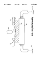
- FIG. 5 is an illustration of another embodiment of a method and apparatus for cooling a semiconductor die in accordance with the teachings of the present invention.
- a semiconductor die 501 is packaged in a C4 package 503, which is mounted in a socket 505 mounted on a circuit board 507. Similar to the system described with respect to FIG. 1B, semiconductor die 501 may be operated in the vacuum chamber of an e-beam probing system for silicon debug and fault isolation purposes.
- a cooling plate 513 having an opening 515 is disposed over and thermally coupled to semiconductor die 501. Opening 515 is disposed over a back side surface 511 of semiconductor die 501 thus providing direct and unobstructed access for a probe tool 509 to the exposed portion of the back side surface 511 of semiconductor die 501.
- a malleable thermal conductor such as indium 517 is disposed between semiconductor die 501 and cooling plate 513 in the interface contact region to provide a conformable thermal contact between semiconductor die 501 and cooling plate 513 such that the thermal coupling between semiconductor die 501 and cooling plate 513 is increased. Therefore, the heat generated by semiconductor die 501 while operating at full intended operating speeds is transferred to cooling plate 513 through indium 517.
- the present invention may be compatible with the temperature control systems of present day e-beam probing systems in which a cooling block 519 is disposed on the opposite side of circuit board 507.
- a cooling block 519 is disposed on the opposite side of circuit board 507.
- probe tool 509 probes semiconductor die 501, which is mounted on circuit board 507.
- cooling block 519 is located on the opposite side of circuit board 507 as is the case with many existing e-beam probing systems that are configured to probe wire bond packaged integrated circuits.
- cooling plate 513 is thermally coupled to cooling block 519 through heat transfer conduits 523A and 523B.
- heat transfer conduits 523A-B include thermal screws that extend from cooling plate 513 through openings 525A and 525B respectively in circuit board 507 to cooling block 519.
- cooling block 519 includes threaded holes 529A and 529B configured to receive the threads 527A and 527B of heat transfer conduits 523A and 523B respectively.
- heat transfer conduits 523A and 523B thermally couple cooling plate 513 to cooling block 519 such that heat is transferred from semiconductor die 501 through cooling plate 513, through heat transfer conduits 523A-B to cooling block 519.
- the thermal screws of heat transfer conduits 523A and 523B include oversized heads 531A and 531B respectively as well as oversized threads 527A and 527B respectively.
- the thermal screws of heat transfer conduits 523A and 523B include oversized heads 531A and 531B respectively as well as oversized threads 527A and 527B respectively.
- the amount of surface area in which heat transfer conduits 523A and 523B are in thermal contact with cooling plate 513 is increased so as to decrease thermal resistance as well as increase thermal conductivity.
- the oversized threads 527A and 527B the amount of surface area in which heat transfer conduits 523A and 523B are in thermal contact with cooling block 519 is increased therefore reducing thermal resistance and increasing thermal conductivity.
- cooling plate 513 includes features 533A and 533B located on circuit board 507 side of cooling plate 513 such that features 533A and 533B tend to push C4 package 503 into socket 505 of circuit board 507 when the thermal screws of heat transfer conduits 523A and 523B are tightened. As such, it is more likely that C4 package 503 is properly seated in socket 505 after thermal screws of heat transfer conduits 523A and 523B are tightened.
- the thermal screws of heat transfer conduits 523A and 523B also allow adjusting of the plane of cooling plate 513 to the plane of the back side surface 511 of semiconductor die 501 so as to further increase thermal contact through indium 517.
- cooling plate 513 includes copper with a nickel coating.
- the thermal screws of heat transfer conduits 523A and 523B are also made of copper. It is recognized that copper is particularly well suited for the present application since copper is a good thermal conductor. It is noted however that the present invention is not limited to a cooling plate 513 and heat transfer conduits 523A and 523B that are made of copper and that other materials may therefore be used so long as cooling plate 513 and heat transfer conduits 523A and 523B have sufficient thermal conductivity to cool semiconductor die 501 in accordance with the teachings of the present invention.
- coolant 521 is circulated through cooling block 519 to further facilitate the removal of heat from semiconductor die 501.
- C4 mounted integrated circuits or MCM units may be operated in a vacuum chamber of an e-beam probing system for a silicon debug and fault isolation.
- the presently described cooling method and apparatus also provide cooling to C4 mounted integrated circuits or MCM units operated outside a vacuum chamber during laser based tests or mechanical probing.
- the presently described apparatus and method cool the semiconductor die without relying upon thermal conduction through package and without significantly obscuring the exposed circuit substrate of the C4 or MCM units.
- the present invention is compatible with existing temperature control systems in present day e-beam probing systems typically configured to cool the semiconductor dies through their respective packages.
Abstract
Description
Claims (27)
Priority Applications (7)
| Application Number | Priority Date | Filing Date | Title |
|---|---|---|---|
| US08/856,267 US5923086A (en) | 1997-05-14 | 1997-05-14 | Apparatus for cooling a semiconductor die |
| KR10-1999-7010524A KR100381431B1 (en) | 1997-05-14 | 1998-04-14 | Method and apparatus for cooling a semiconductor die |
| AU69718/98A AU6971898A (en) | 1997-05-14 | 1998-04-14 | Method and apparatus for cooling a semiconductor die |
| CNB988070995A CN1154180C (en) | 1997-05-14 | 1998-04-14 | Method and apparatus for cooling semiconductor die |
| JP54923498A JP4040695B2 (en) | 1997-05-14 | 1998-04-14 | Device for cooling semiconductor dies |
| PCT/US1998/007490 WO1998052223A1 (en) | 1997-05-14 | 1998-04-14 | Method and apparatus for cooling a semiconductor die |
| MYPI98002128A MY114590A (en) | 1997-05-14 | 1998-05-13 | Apparatus for cooling a semiconductor die |
Applications Claiming Priority (1)
| Application Number | Priority Date | Filing Date | Title |
|---|---|---|---|
| US08/856,267 US5923086A (en) | 1997-05-14 | 1997-05-14 | Apparatus for cooling a semiconductor die |
Publications (1)
| Publication Number | Publication Date |
|---|---|
| US5923086A true US5923086A (en) | 1999-07-13 |
Family
ID=25323202
Family Applications (1)
| Application Number | Title | Priority Date | Filing Date |
|---|---|---|---|
| US08/856,267 Expired - Lifetime US5923086A (en) | 1997-05-14 | 1997-05-14 | Apparatus for cooling a semiconductor die |
Country Status (7)
| Country | Link |
|---|---|
| US (1) | US5923086A (en) |
| JP (1) | JP4040695B2 (en) |
| KR (1) | KR100381431B1 (en) |
| CN (1) | CN1154180C (en) |
| AU (1) | AU6971898A (en) |
| MY (1) | MY114590A (en) |
| WO (1) | WO1998052223A1 (en) |
Cited By (29)
| Publication number | Priority date | Publication date | Assignee | Title |
|---|---|---|---|---|
| US6043560A (en) * | 1997-12-03 | 2000-03-28 | Intel Corporation | Thermal interface thickness control for a microprocessor |
| WO2001020673A1 (en) * | 1999-09-13 | 2001-03-22 | Intel Corporation | A method of constructing an electronic assembly having an indium thermal couple and an electronic assembly having an indium thermal couple |
| US6317326B1 (en) * | 2000-09-14 | 2001-11-13 | Sun Microsystems, Inc. | Integrated circuit device package and heat dissipation device |
| US6364669B1 (en) * | 2000-07-12 | 2002-04-02 | Advanced Micro Devices, Inc. | Spring contact for providing high current power to an integrated circuit |
| US6372997B1 (en) | 2000-02-25 | 2002-04-16 | Thermagon, Inc. | Multi-layer structure and method for forming a thermal interface with low contact resistance between a microelectronic component package and heat sink |
| US20020114567A1 (en) * | 2001-02-07 | 2002-08-22 | Lukas Novotny | System and method for high resolution optical imaging, data storage, lithography, and inspection |
| US6467679B2 (en) * | 1999-07-02 | 2002-10-22 | Kabushiki Kaisha Shinkawa | Wire bonding method |
| FR2826508A1 (en) * | 2001-06-20 | 2002-12-27 | Alstom | ELECTRONIC POWER MODULE AND POWER COMPONENT FOR FITTING SUCH A MODULE |
| US6504242B1 (en) | 2001-11-15 | 2003-01-07 | Intel Corporation | Electronic assembly having a wetting layer on a thermally conductive heat spreader |
| US6545351B1 (en) | 1998-07-21 | 2003-04-08 | Intel Corporation | Underside heat slug for ball grid array packages |
| US6545346B2 (en) | 2001-03-23 | 2003-04-08 | Intel Corporation | Integrated circuit package with a capacitor |
| US6558169B2 (en) | 2001-03-29 | 2003-05-06 | Intel Corporation | Shunt power connection for an integrated circuit package |
| US20040065880A1 (en) * | 2002-10-03 | 2004-04-08 | Schlumberger Technologies, Inc. | Optical testing of integrated circuits with temperature control |
| US6761211B2 (en) | 2000-03-14 | 2004-07-13 | Delphi Technologies, Inc. | High-performance heat sink for electronics cooling |
| US6771500B1 (en) * | 2003-03-27 | 2004-08-03 | Stmicroelectronics, Inc. | System and method for direct convective cooling of an exposed integrated circuit die surface |
| US6888722B2 (en) * | 1999-12-30 | 2005-05-03 | Intel Corporation | Thermal design for minimizing interface in a multi-site thermal contact condition |
| US20050270742A1 (en) * | 2004-06-04 | 2005-12-08 | Cooligy, Inc. | Semi-compliant joining mechanism for semiconductor cooling applications |
| US20060164807A1 (en) * | 2005-01-21 | 2006-07-27 | Ilya Reyzin | Apparatus for controlling thermal interface between cold plate and integrated circuit chip |
| US20070125526A1 (en) * | 2005-12-02 | 2007-06-07 | Matsushita Electric Industrial Co., Ltd. | Cooling device for electronic components |
| US20070211431A1 (en) * | 2004-06-04 | 2007-09-13 | Cooligy Inc. | Gimballed attachment for multiple heat exchangers |
| US20090179322A1 (en) * | 2007-12-12 | 2009-07-16 | International Business Machines Corporation | Electronic package method and structure with cure-melt hierarchy |
| US7715194B2 (en) | 2006-04-11 | 2010-05-11 | Cooligy Inc. | Methodology of cooling multiple heat sources in a personal computer through the use of multiple fluid-based heat exchanging loops coupled via modular bus-type heat exchangers |
| US7913719B2 (en) | 2006-01-30 | 2011-03-29 | Cooligy Inc. | Tape-wrapped multilayer tubing and methods for making the same |
| US8157001B2 (en) | 2006-03-30 | 2012-04-17 | Cooligy Inc. | Integrated liquid to air conduction module |
| US8250877B2 (en) | 2008-03-10 | 2012-08-28 | Cooligy Inc. | Device and methodology for the removal of heat from an equipment rack by means of heat exchangers mounted to a door |
| US20140118735A1 (en) * | 2012-10-25 | 2014-05-01 | Shimadzu Corporation | High-frequency power supply for plasma and icp optical emission spectrometer using the same |
| US20150333032A1 (en) * | 2012-12-05 | 2015-11-19 | Shinkawa Ltd. | Bonding tool cooling apparatus and method for cooling bonding tool |
| US20150380381A1 (en) * | 2013-03-12 | 2015-12-31 | Shinkawa Ltd. | Flip chip bonder and flip chip bonding method |
| US9297571B1 (en) | 2008-03-10 | 2016-03-29 | Liebert Corporation | Device and methodology for the removal of heat from an equipment rack by means of heat exchangers mounted to a door |
Families Citing this family (5)
| Publication number | Priority date | Publication date | Assignee | Title |
|---|---|---|---|---|
| JP4607445B2 (en) * | 2003-11-04 | 2011-01-05 | 浜松ホトニクス株式会社 | Temperature control device and microscope stand |
| CN102316699B (en) * | 2010-07-07 | 2015-10-14 | 富泰华工业(深圳)有限公司 | Cooling means, the circuit board repair device using this cooling device method and equipment |
| KR101343233B1 (en) * | 2011-11-28 | 2013-12-18 | 삼성전기주식회사 | Power Module Package |
| CN102788945A (en) * | 2012-07-19 | 2012-11-21 | 中国科学院电工研究所 | Universal power semiconductor module fixture |
| CN108626331B (en) | 2017-03-21 | 2021-03-02 | 株式会社椿本链条 | Tension device |
Citations (23)
| Publication number | Priority date | Publication date | Assignee | Title |
|---|---|---|---|---|
| US3654528A (en) * | 1970-08-03 | 1972-04-04 | Gen Electric | Cooling scheme for a high-current semiconductor device employing electromagnetically-pumped liquid metal for heat and current transfer |
| US3990100A (en) * | 1974-10-09 | 1976-11-02 | Sony Corporation | Semiconductor device having an antireflective coating |
| US4168113A (en) * | 1977-07-05 | 1979-09-18 | American Optical Corporation | Glass lens with ion-exchanged antireflection coating and process for manufacture thereof |
| US4529685A (en) * | 1984-03-02 | 1985-07-16 | Advanced Micro Devices, Inc. | Method for making integrated circuit devices using a layer of indium arsenide as an antireflective coating |
| US4582954A (en) * | 1983-10-26 | 1986-04-15 | Plessey Overseas Limited | Diamond heatsink assemblies |
| US4617252A (en) * | 1983-07-01 | 1986-10-14 | Philip A. Hunt Chemical Corporation | Antireflective coatings for use in the manufacture of semi-conductor devices, methods and solutions for making such coatings, and the method for using such coatings to absorb light in ultraviolet photolithography processes |
| US4649992A (en) * | 1984-10-05 | 1987-03-17 | Plessey Overseas Limited | Diamond heatsink assemblies |
| US4672422A (en) * | 1981-10-31 | 1987-06-09 | Semikron Gesellschaft Fur Gleichrichterbau Und Elektronik M.B.H. | Semiconductor rectifier unit |
| US5000256A (en) * | 1990-07-20 | 1991-03-19 | Minnesota Mining And Manufacturing Company | Heat transfer bag with thermal via |
| US5001548A (en) * | 1989-03-13 | 1991-03-19 | Coriolis Corporation | Multi-chip module cooling |
| US5004307A (en) * | 1990-04-12 | 1991-04-02 | The Board Of Trustees Of The Leland Stanford Junior University | Near field and solid immersion optical microscope |
| US5061568A (en) * | 1989-12-20 | 1991-10-29 | Monsanto Company | Solar screening assembly |
| US5070040A (en) * | 1990-03-09 | 1991-12-03 | University Of Colorado Foundation, Inc. | Method and apparatus for semiconductor circuit chip cooling |
| US5106786A (en) * | 1989-10-23 | 1992-04-21 | At&T Bell Laboratories | Thin coatings for use in semiconductor integrated circuits and processes as antireflection coatings consisting of tungsten silicide |
| US5146314A (en) * | 1990-03-09 | 1992-09-08 | The University Of Colorado Foundation, Inc. | Apparatus for semiconductor circuit chip cooling using a diamond layer |
| US5243458A (en) * | 1990-12-25 | 1993-09-07 | Minolta Camera Kabushiki Kaisha | Antireflection coating for infrared light |
| US5285351A (en) * | 1991-05-30 | 1994-02-08 | Nec Corporation | Cooling structure for integrated circuits |
| US5354717A (en) * | 1993-07-29 | 1994-10-11 | Motorola, Inc. | Method for making a substrate structure with improved heat dissipation |
| US5376587A (en) * | 1991-05-03 | 1994-12-27 | International Business Machines Corporation | Method for making cooling structures for directly cooling an active layer of a semiconductor chip |
| US5418019A (en) * | 1994-05-25 | 1995-05-23 | Georgia Tech Research Corporation | Method for low temperature plasma enhanced chemical vapor deposition (PECVD) of an oxide and nitride antireflection coating on silicon |
| US5463528A (en) * | 1992-01-22 | 1995-10-31 | Nec Corporation | Cooling structure for integrated circuits |
| US5500540A (en) * | 1994-04-15 | 1996-03-19 | Photonics Research Incorporated | Wafer scale optoelectronic package |
| US5508230A (en) * | 1993-07-29 | 1996-04-16 | Motorola, Inc. | Method for making a semiconductor device with diamond heat dissipation layer |
Family Cites Families (6)
| Publication number | Priority date | Publication date | Assignee | Title |
|---|---|---|---|---|
| US4996589A (en) * | 1987-10-21 | 1991-02-26 | Hitachi, Ltd. | Semiconductor module and cooling device of the same |
| KR900700955A (en) * | 1988-04-08 | 1990-08-17 | 미다 가쓰시게 | Computer using semiconductor module and its cooling system |
| EP0560478B1 (en) * | 1992-02-10 | 1998-10-14 | Nec Corporation | Cooling structure for electronic circuit package |
| JP3326721B2 (en) * | 1992-08-04 | 2002-09-24 | 富士通株式会社 | Cooling device for ceramic substrate |
| JPH07336077A (en) * | 1994-06-14 | 1995-12-22 | Fujitsu Ltd | Cooling structure of heating-element package |
| JP2926537B2 (en) * | 1994-12-15 | 1999-07-28 | 株式会社日立製作所 | Multi-chip module cooling system |
-
1997
- 1997-05-14 US US08/856,267 patent/US5923086A/en not_active Expired - Lifetime
-
1998
- 1998-04-14 KR KR10-1999-7010524A patent/KR100381431B1/en not_active IP Right Cessation
- 1998-04-14 AU AU69718/98A patent/AU6971898A/en not_active Abandoned
- 1998-04-14 JP JP54923498A patent/JP4040695B2/en not_active Expired - Fee Related
- 1998-04-14 WO PCT/US1998/007490 patent/WO1998052223A1/en active IP Right Grant
- 1998-04-14 CN CNB988070995A patent/CN1154180C/en not_active Expired - Fee Related
- 1998-05-13 MY MYPI98002128A patent/MY114590A/en unknown
Patent Citations (23)
| Publication number | Priority date | Publication date | Assignee | Title |
|---|---|---|---|---|
| US3654528A (en) * | 1970-08-03 | 1972-04-04 | Gen Electric | Cooling scheme for a high-current semiconductor device employing electromagnetically-pumped liquid metal for heat and current transfer |
| US3990100A (en) * | 1974-10-09 | 1976-11-02 | Sony Corporation | Semiconductor device having an antireflective coating |
| US4168113A (en) * | 1977-07-05 | 1979-09-18 | American Optical Corporation | Glass lens with ion-exchanged antireflection coating and process for manufacture thereof |
| US4672422A (en) * | 1981-10-31 | 1987-06-09 | Semikron Gesellschaft Fur Gleichrichterbau Und Elektronik M.B.H. | Semiconductor rectifier unit |
| US4617252A (en) * | 1983-07-01 | 1986-10-14 | Philip A. Hunt Chemical Corporation | Antireflective coatings for use in the manufacture of semi-conductor devices, methods and solutions for making such coatings, and the method for using such coatings to absorb light in ultraviolet photolithography processes |
| US4582954A (en) * | 1983-10-26 | 1986-04-15 | Plessey Overseas Limited | Diamond heatsink assemblies |
| US4529685A (en) * | 1984-03-02 | 1985-07-16 | Advanced Micro Devices, Inc. | Method for making integrated circuit devices using a layer of indium arsenide as an antireflective coating |
| US4649992A (en) * | 1984-10-05 | 1987-03-17 | Plessey Overseas Limited | Diamond heatsink assemblies |
| US5001548A (en) * | 1989-03-13 | 1991-03-19 | Coriolis Corporation | Multi-chip module cooling |
| US5106786A (en) * | 1989-10-23 | 1992-04-21 | At&T Bell Laboratories | Thin coatings for use in semiconductor integrated circuits and processes as antireflection coatings consisting of tungsten silicide |
| US5061568A (en) * | 1989-12-20 | 1991-10-29 | Monsanto Company | Solar screening assembly |
| US5146314A (en) * | 1990-03-09 | 1992-09-08 | The University Of Colorado Foundation, Inc. | Apparatus for semiconductor circuit chip cooling using a diamond layer |
| US5070040A (en) * | 1990-03-09 | 1991-12-03 | University Of Colorado Foundation, Inc. | Method and apparatus for semiconductor circuit chip cooling |
| US5004307A (en) * | 1990-04-12 | 1991-04-02 | The Board Of Trustees Of The Leland Stanford Junior University | Near field and solid immersion optical microscope |
| US5000256A (en) * | 1990-07-20 | 1991-03-19 | Minnesota Mining And Manufacturing Company | Heat transfer bag with thermal via |
| US5243458A (en) * | 1990-12-25 | 1993-09-07 | Minolta Camera Kabushiki Kaisha | Antireflection coating for infrared light |
| US5376587A (en) * | 1991-05-03 | 1994-12-27 | International Business Machines Corporation | Method for making cooling structures for directly cooling an active layer of a semiconductor chip |
| US5285351A (en) * | 1991-05-30 | 1994-02-08 | Nec Corporation | Cooling structure for integrated circuits |
| US5463528A (en) * | 1992-01-22 | 1995-10-31 | Nec Corporation | Cooling structure for integrated circuits |
| US5354717A (en) * | 1993-07-29 | 1994-10-11 | Motorola, Inc. | Method for making a substrate structure with improved heat dissipation |
| US5508230A (en) * | 1993-07-29 | 1996-04-16 | Motorola, Inc. | Method for making a semiconductor device with diamond heat dissipation layer |
| US5500540A (en) * | 1994-04-15 | 1996-03-19 | Photonics Research Incorporated | Wafer scale optoelectronic package |
| US5418019A (en) * | 1994-05-25 | 1995-05-23 | Georgia Tech Research Corporation | Method for low temperature plasma enhanced chemical vapor deposition (PECVD) of an oxide and nitride antireflection coating on silicon |
Non-Patent Citations (6)
| Title |
|---|
| D. Voorhes, "Liquid Cooling for DPSS Lasers", Lasers & Optronics, Aug., 1996. |
| D. Voorhes, Liquid Cooling for DPSS Lasers , Lasers & Optronics , Aug., 1996. * |
| D.L. Barton, "Infrared Light Emission from Semiconductor Devices", Proc. of the 22nd Internat. Symp. for Testing and Failure Analysis, pp. 9-17, Nov. 18-22, Los Angeles, CA, Nov. 1996. |
| D.L. Barton, Infrared Light Emission from Semiconductor Devices , Proc. of the 22nd Internat. Symp. for Testing and Failure Analysis , pp. 9 17, Nov. 18 22, Los Angeles, CA, Nov. 1996. * |
| S. Hayashi, "Solid Immersion Lens for Optical Storage", SPIE Symp. on Electronic Imaging Science & Technology, Report No. 5285, Feb. 5-10, 1995. |
| S. Hayashi, Solid Immersion Lens for Optical Storage , SPIE Symp. on Electronic Imaging Science & Technology , Report No. 5285, Feb. 5 10, 1995. * |
Cited By (47)
| Publication number | Priority date | Publication date | Assignee | Title |
|---|---|---|---|---|
| US6043560A (en) * | 1997-12-03 | 2000-03-28 | Intel Corporation | Thermal interface thickness control for a microprocessor |
| US6545351B1 (en) | 1998-07-21 | 2003-04-08 | Intel Corporation | Underside heat slug for ball grid array packages |
| US6491202B1 (en) * | 1999-07-02 | 2002-12-10 | Kabushiki Kaisha Shinkawa | Wire bonding apparatus and method |
| US6467679B2 (en) * | 1999-07-02 | 2002-10-22 | Kabushiki Kaisha Shinkawa | Wire bonding method |
| CN1319158C (en) * | 1999-09-13 | 2007-05-30 | 英特尔公司 | Method of constructing electronic assembly having indium thermal couple and electronic assembly having indium thermal couple |
| US6461891B1 (en) | 1999-09-13 | 2002-10-08 | Intel Corporation | Method of constructing an electronic assembly having an indium thermal couple and an electronic assembly having an indium thermal couple |
| US6882043B2 (en) | 1999-09-13 | 2005-04-19 | Intel Corporation | Electronic assembly having an indium thermal couple |
| WO2001020673A1 (en) * | 1999-09-13 | 2001-03-22 | Intel Corporation | A method of constructing an electronic assembly having an indium thermal couple and an electronic assembly having an indium thermal couple |
| US6888722B2 (en) * | 1999-12-30 | 2005-05-03 | Intel Corporation | Thermal design for minimizing interface in a multi-site thermal contact condition |
| US6372997B1 (en) | 2000-02-25 | 2002-04-16 | Thermagon, Inc. | Multi-layer structure and method for forming a thermal interface with low contact resistance between a microelectronic component package and heat sink |
| US6617517B2 (en) | 2000-02-25 | 2003-09-09 | Thermagon, Inc. | Multi-layer structure having a thermal interface with low contact resistance between a microelectronic component package and a heat sink |
| US6761211B2 (en) | 2000-03-14 | 2004-07-13 | Delphi Technologies, Inc. | High-performance heat sink for electronics cooling |
| US6364669B1 (en) * | 2000-07-12 | 2002-04-02 | Advanced Micro Devices, Inc. | Spring contact for providing high current power to an integrated circuit |
| US6317326B1 (en) * | 2000-09-14 | 2001-11-13 | Sun Microsystems, Inc. | Integrated circuit device package and heat dissipation device |
| US7526158B2 (en) | 2001-02-07 | 2009-04-28 | University Of Rochester | System and method for high resolution optical imaging, data storage, lithography, and inspection |
| US20020114567A1 (en) * | 2001-02-07 | 2002-08-22 | Lukas Novotny | System and method for high resolution optical imaging, data storage, lithography, and inspection |
| US6545346B2 (en) | 2001-03-23 | 2003-04-08 | Intel Corporation | Integrated circuit package with a capacitor |
| US6558169B2 (en) | 2001-03-29 | 2003-05-06 | Intel Corporation | Shunt power connection for an integrated circuit package |
| FR2826508A1 (en) * | 2001-06-20 | 2002-12-27 | Alstom | ELECTRONIC POWER MODULE AND POWER COMPONENT FOR FITTING SUCH A MODULE |
| US6738253B2 (en) | 2001-06-20 | 2004-05-18 | Alstom | Electronic power module and a power component designed to equip such a module |
| EP1271646A3 (en) * | 2001-06-20 | 2005-12-14 | Alstom | Electronic power module and power component for such a module |
| EP1271646A2 (en) * | 2001-06-20 | 2003-01-02 | Alstom | Electronic power module and power component for such a module |
| US6504242B1 (en) | 2001-11-15 | 2003-01-07 | Intel Corporation | Electronic assembly having a wetting layer on a thermally conductive heat spreader |
| US20050168212A1 (en) * | 2002-10-03 | 2005-08-04 | Credence Systems Corporation | Optical testing of integrated circuits with temperature control |
| US6836014B2 (en) | 2002-10-03 | 2004-12-28 | Credence Systems Corporation | Optical testing of integrated circuits with temperature control |
| US7064568B2 (en) | 2002-10-03 | 2006-06-20 | Credence Systems Corporation | Optical testing of integrated circuits with temperature control |
| US20040065880A1 (en) * | 2002-10-03 | 2004-04-08 | Schlumberger Technologies, Inc. | Optical testing of integrated circuits with temperature control |
| US6771500B1 (en) * | 2003-03-27 | 2004-08-03 | Stmicroelectronics, Inc. | System and method for direct convective cooling of an exposed integrated circuit die surface |
| US20050270742A1 (en) * | 2004-06-04 | 2005-12-08 | Cooligy, Inc. | Semi-compliant joining mechanism for semiconductor cooling applications |
| US7301773B2 (en) | 2004-06-04 | 2007-11-27 | Cooligy Inc. | Semi-compliant joining mechanism for semiconductor cooling applications |
| US20070211431A1 (en) * | 2004-06-04 | 2007-09-13 | Cooligy Inc. | Gimballed attachment for multiple heat exchangers |
| US7280363B2 (en) * | 2005-01-21 | 2007-10-09 | Delphi Technologies, Inc. | Apparatus for controlling thermal interface between cold plate and integrated circuit chip |
| US20060164807A1 (en) * | 2005-01-21 | 2006-07-27 | Ilya Reyzin | Apparatus for controlling thermal interface between cold plate and integrated circuit chip |
| US20070125526A1 (en) * | 2005-12-02 | 2007-06-07 | Matsushita Electric Industrial Co., Ltd. | Cooling device for electronic components |
| US7913719B2 (en) | 2006-01-30 | 2011-03-29 | Cooligy Inc. | Tape-wrapped multilayer tubing and methods for making the same |
| US8157001B2 (en) | 2006-03-30 | 2012-04-17 | Cooligy Inc. | Integrated liquid to air conduction module |
| US7715194B2 (en) | 2006-04-11 | 2010-05-11 | Cooligy Inc. | Methodology of cooling multiple heat sources in a personal computer through the use of multiple fluid-based heat exchanging loops coupled via modular bus-type heat exchangers |
| US7834442B2 (en) | 2007-12-12 | 2010-11-16 | International Business Machines Corporation | Electronic package method and structure with cure-melt hierarchy |
| US20090179322A1 (en) * | 2007-12-12 | 2009-07-16 | International Business Machines Corporation | Electronic package method and structure with cure-melt hierarchy |
| US8250877B2 (en) | 2008-03-10 | 2012-08-28 | Cooligy Inc. | Device and methodology for the removal of heat from an equipment rack by means of heat exchangers mounted to a door |
| US9297571B1 (en) | 2008-03-10 | 2016-03-29 | Liebert Corporation | Device and methodology for the removal of heat from an equipment rack by means of heat exchangers mounted to a door |
| US20140118735A1 (en) * | 2012-10-25 | 2014-05-01 | Shimadzu Corporation | High-frequency power supply for plasma and icp optical emission spectrometer using the same |
| US10327320B2 (en) * | 2012-10-25 | 2019-06-18 | Shimadzu Corporation | High-frequency power supply for plasma and ICP optical emission spectrometer using the same |
| US20150333032A1 (en) * | 2012-12-05 | 2015-11-19 | Shinkawa Ltd. | Bonding tool cooling apparatus and method for cooling bonding tool |
| US9576927B2 (en) * | 2012-12-05 | 2017-02-21 | Shinkawa Ltd. | Bonding tool cooling apparatus and method for cooling bonding tool |
| US20150380381A1 (en) * | 2013-03-12 | 2015-12-31 | Shinkawa Ltd. | Flip chip bonder and flip chip bonding method |
| US9536856B2 (en) * | 2013-03-12 | 2017-01-03 | Shinkawa Ltd. | Flip chip bonder and flip chip bonding method |
Also Published As
| Publication number | Publication date |
|---|---|
| CN1263638A (en) | 2000-08-16 |
| CN1154180C (en) | 2004-06-16 |
| MY114590A (en) | 2002-11-30 |
| WO1998052223A1 (en) | 1998-11-19 |
| JP2001526838A (en) | 2001-12-18 |
| AU6971898A (en) | 1998-12-08 |
| JP4040695B2 (en) | 2008-01-30 |
| KR20010012569A (en) | 2001-02-15 |
| KR100381431B1 (en) | 2003-04-23 |
Similar Documents
| Publication | Publication Date | Title |
|---|---|---|
| US5923086A (en) | Apparatus for cooling a semiconductor die | |
| US5396403A (en) | Heat sink assembly with thermally-conductive plate for a plurality of integrated circuits on a substrate | |
| US5430611A (en) | Spring-biased heat sink assembly for a plurality of integrated circuits on a substrate | |
| US4034469A (en) | Method of making conduction-cooled circuit package | |
| US7967062B2 (en) | Thermally conductive composite interface, cooled electronic assemblies employing the same, and methods of fabrication thereof | |
| US7768121B2 (en) | Apparatus and methods for cooling semiconductor integrated circuit package structures | |
| US6483708B2 (en) | Heatsink apparatus for de-coupling clamping forces on an integrated circuit package | |
| US5367193A (en) | Low cost, thermally efficient, and surface mountable semiconductor package for a high applied power VLSI die | |
| EP0871352B1 (en) | Integrated circuit device cooling structure | |
| US6191478B1 (en) | Demountable heat spreader and high reliability flip chip package assembly | |
| CA2139266C (en) | Semiconductor package | |
| US6570247B1 (en) | Integrated circuit device having an embedded heat slug | |
| JPH07507182A (en) | 3D multi-chip module | |
| US4897764A (en) | Conductive cooling cup module | |
| US7355276B1 (en) | Thermally-enhanced circuit assembly | |
| US7151308B2 (en) | Semiconductor chip package | |
| JPH1168360A (en) | Cooling structure for semiconductor element | |
| JPH09213847A (en) | Semiconductor integrated circuit device, manufacture thereof, and electronic device equipped therewith | |
| MXPA99010188A (en) | Method and apparatus for cooling a semiconductor die | |
| JPS63289847A (en) | Heat dissipation structure of lsi package | |
| JPS62224053A (en) | Semiconductor device with cooling system | |
| TW202336471A (en) | Thermal management techniques for high power integrated circuits operating in dry cryogenic environments | |
| JPH11297911A (en) | Semiconductor device and its manufacture | |
| JPH04139754A (en) | Cooler | |
| JPH0897251A (en) | Tab tape |
Legal Events
| Date | Code | Title | Description |
|---|---|---|---|
| AS | Assignment |
Owner name: INTEL CORPORATION, CALIFORNIA Free format text: ASSIGNMENT OF ASSIGNORS INTEREST;ASSIGNORS:WINER, PAUL;PANICCIA, MARIO J.;MA, KARL J.;REEL/FRAME:008617/0087 Effective date: 19970513 |
|
| AS | Assignment |
Owner name: INTEL CORPORATION, CALIFORNIA Free format text: ASSIGNMENT OF ASSIGNORS INTEREST;ASSIGNOR:MA, KARL J.;REEL/FRAME:008680/0237 Effective date: 19970520 |
|
| STCF | Information on status: patent grant |
Free format text: PATENTED CASE |
|
| FPAY | Fee payment |
Year of fee payment: 4 |
|
| FPAY | Fee payment |
Year of fee payment: 8 |
|
| FPAY | Fee payment |
Year of fee payment: 12 |