US5923177A - Portable wedge probe for perusing signals on the pins of an IC - Google Patents
Portable wedge probe for perusing signals on the pins of an IC Download PDFInfo
- Publication number
- US5923177A US5923177A US08/825,081 US82508197A US5923177A US 5923177 A US5923177 A US 5923177A US 82508197 A US82508197 A US 82508197A US 5923177 A US5923177 A US 5923177A
- Authority
- US
- United States
- Prior art keywords
- wedges
- probe
- pins
- wedge
- row
- Prior art date
- Legal status (The legal status is an assumption and is not a legal conclusion. Google has not performed a legal analysis and makes no representation as to the accuracy of the status listed.)
- Expired - Fee Related
Links
- 239000000523 sample Substances 0.000 title claims abstract description 44
- 239000004020 conductor Substances 0.000 claims description 7
- 238000004382 potting Methods 0.000 claims description 4
- 150000001875 compounds Chemical class 0.000 claims 1
- 125000006850 spacer group Chemical group 0.000 claims 1
- 238000012360 testing method Methods 0.000 abstract description 10
- 238000005259 measurement Methods 0.000 abstract description 4
- 230000009977 dual effect Effects 0.000 abstract description 3
- 238000007689 inspection Methods 0.000 abstract description 2
- 239000004593 Epoxy Substances 0.000 description 4
- 229910000679 solder Inorganic materials 0.000 description 4
- 230000009471 action Effects 0.000 description 2
- 229940125898 compound 5 Drugs 0.000 description 2
- 238000004519 manufacturing process Methods 0.000 description 2
- 239000000463 material Substances 0.000 description 2
- 238000000034 method Methods 0.000 description 2
- 229910001369 Brass Inorganic materials 0.000 description 1
- 238000009825 accumulation Methods 0.000 description 1
- 239000000853 adhesive Substances 0.000 description 1
- 230000001070 adhesive effect Effects 0.000 description 1
- 238000013459 approach Methods 0.000 description 1
- 239000010951 brass Substances 0.000 description 1
- 238000007796 conventional method Methods 0.000 description 1
- 230000000694 effects Effects 0.000 description 1
- PCHJSUWPFVWCPO-UHFFFAOYSA-N gold Chemical compound [Au] PCHJSUWPFVWCPO-UHFFFAOYSA-N 0.000 description 1
- 239000010931 gold Substances 0.000 description 1
- 229910052737 gold Inorganic materials 0.000 description 1
- 230000008676 import Effects 0.000 description 1
- 230000006872 improvement Effects 0.000 description 1
- 239000011810 insulating material Substances 0.000 description 1
- 238000009413 insulation Methods 0.000 description 1
- 239000012212 insulator Substances 0.000 description 1
- 238000002955 isolation Methods 0.000 description 1
- 238000012423 maintenance Methods 0.000 description 1
- 239000002184 metal Substances 0.000 description 1
- 229910052751 metal Inorganic materials 0.000 description 1
- 230000029052 metamorphosis Effects 0.000 description 1
- 238000012986 modification Methods 0.000 description 1
- 230000004048 modification Effects 0.000 description 1
- 230000010355 oscillation Effects 0.000 description 1
- 238000004806 packaging method and process Methods 0.000 description 1
- 230000035515 penetration Effects 0.000 description 1
- 230000008569 process Effects 0.000 description 1
- 230000004044 response Effects 0.000 description 1
Images

Classifications
-
- G—PHYSICS
- G01—MEASURING; TESTING
- G01R—MEASURING ELECTRIC VARIABLES; MEASURING MAGNETIC VARIABLES
- G01R1/00—Details of instruments or arrangements of the types included in groups G01R5/00 - G01R13/00 and G01R31/00
- G01R1/02—General constructional details
- G01R1/06—Measuring leads; Measuring probes
- G01R1/067—Measuring probes
- G01R1/06788—Hand-held or hand-manipulated probes, e.g. for oscilloscopes or for portable test instruments
-
- G—PHYSICS
- G01—MEASURING; TESTING
- G01R—MEASURING ELECTRIC VARIABLES; MEASURING MAGNETIC VARIABLES
- G01R1/00—Details of instruments or arrangements of the types included in groups G01R5/00 - G01R13/00 and G01R31/00
- G01R1/02—General constructional details
- G01R1/06—Measuring leads; Measuring probes
- G01R1/067—Measuring probes
- G01R1/06711—Probe needles; Cantilever beams; "Bump" contacts; Replaceable probe pins
Definitions
- test equipment e.g., a voltmeter or an oscilloscope
- test equipment e.g., a voltmeter or an oscilloscope
- These settings include the laboratory, the production floor, and the maintenance shop.
- a variety of "DIP clips" have been produced to facilitate this for the venerable dual in-line package. More recent packaging styles having a high number of closely spaced pins on all four sides of the IC's package have made it nearly imperative that all but the most casual (or the most desperate?) probing be performed with the aid of some special tool. This is because it is difficult to locate or identify a particular pin or pins out the many, and because it is physically difficult to maintain proper contact with the probe tip.
- the (Wardwell) wedge connector comprises tapered fingers of conductive metal separated by an insulator.
- the tapered fingers are wedge-shaped, in that they are thinnest at their tips, so that they may more easily enter the space between adjacent legs of an IC.
- a row of tapered wedges i.e., tapered fingers
- the legs of the IC also form a row with an amount of inter-leg spacing between the legs along the direction of the row.
- the IC legs have sides that face each other along the direction of the row, and that are separated by the amount of the inter-leg spacing.
- the left-hand side of a wedge entering a particular inter-leg space will come into electrical contact with the right-hand side of the IC leg on the left of that inter-leg space, and the right-hand side of that wedge will come into electrical contact with left-hand side of the IC leg on the right of that inter-leg space.
- the thicker parts of the wedge enter the inter-leg space, filling it completely and causing good wiping action and firm contact pressure between the sides of the IC legs and the sides of the wedges.
- each wedge is electrically connected to the right-hand side of its neighboring wedge on the right, which, by implication means that the right-hand side of each wedge is also electrically connected to the left-hand side of its neighboring wedge to the right.
- This interconnectedness of the wedges in a row thereof produces a very desirable effect: if there are n-many legs on the IC and n+1 wedges in a row, then each leg of the IC is in electrical contact at two different places with two different wedges. This adds a robust reliability to the wedge connector.
- the wedges interdigitate with the facing sides of adjacent legs of the IC, and that no attempt is made to produce contact with the outer faces of the legs of the IC; instead, the wedges pass between the legs.
- Wedge compliance can be improved by fabricating the wedges with air gaps between those portions of their internal layers of material that correspond to the tapered portions of the wedge. This makes the wedges more compressible over their tapered region, as well as somewhat more bendable in the side-to-side direction. Correct initial interdigitation is enhanced by beveling the ends of the conductive surfaces at the tips of the wedges. This reduces the cross section of the wedges, making them “sharper” so that they more easily engage the empty inter-leg spaces. Solder debris accumulation is reduced by having a center piece of insulating material at the central core of the wedge extend beyond the tapered end of the wedge by a small amount, say ten thousandths of an inch. The beveling of the conductive sides of the tapered wedges also assists with solder debris abatement, as sharper edges present less of a shelf with which to gouge the solder and carry a build-up of scraped off solder debris.
- the various wedge contact apparatus disclosed in the incorporated patents to Wardwell, and summarized above are all oriented around making simultaneous contact with, if not each and every pin on the IC, at least a large number of pins, and, if not from all four sides of a quad flat pack, at least from two different sides.
- the task at hand requires probing only one or a relatively few number of pins at a time.
- the strategy of wedging between the pins or legs of an IC to obtain electrical contact is an attractive one for many reasons, most of which are set out in Wardwell's patents.
- the wedge probe technique could be adapted to making simultaneous contact (for probing) with one, two, or some other small number of adjacent pins or legs of an IC, and for readily changing the location on the IC of where such simultaneous contact occurred, almost as readily as one deploys a scope probe on a low density printed circuit board loaded with discrete parts. That is, it would be desirable if a wedge probe for electrically connecting to just one or to a limited and relatively small number of pins on an IC were "portable", in the sense that it is readily re-deployable at different locations on the IC.
- Such a wedge probe would have far fewer wedges than needed to simultaneously connect to every pin on the IC, and would allow an easy perusal of the IC's signals by simply repositioning the probe. Such a portable wedge probe would also be less expensive than its full sized counterpart.
- a portable wedge probe for perusing the signals of an IC may be produced by mounting a short row of wedges in a housing that serves the dual purposes of: (1) Allowing the griping and manipulation of the wedges for inspection, the connecting and unconnecting of interconnecting cables, deployment onto, and removal from, the IC; and (2) serving as the housing for and physical location of electrical interconnection(s) between the portable wedge probe and the cable(s) of the measurement (test) equipment.
- short row of wedges we mean, say, two adjacent wedges for the signal on a single intervening interior pin of the IC, up to perhaps nine adjacent wedges for the eight signals on the eight intervening interior pins of the IC.
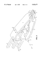
- FIG. 1 is a top view of one embodiment of a portable wedge probe for perusing the signals on the pins of an IC
- FIG. 2 is a an enlarged perspective side view of the portable wedge probe of FIG. 1.
- the embodiment 1 includes a housing 3 that seats a row of tapered wedges 4 and a number (in this case, three) of gold plated brass pins 6, 7 and 8 to which are attached flexible insulated wires 13 and 14 that connect to the test equipment that is to perform the desired measurement.
- a row of tapered wedges 4 and a number (in this case, three) of gold plated brass pins 6, 7 and 8 to which are attached flexible insulated wires 13 and 14 that connect to the test equipment that is to perform the desired measurement.
- To deploy and use the probe 2 it is positioned just above a row of legs or pins of an IC (not shown) and then pressed downward to cause interdigitation of the tapered wedges with the legs of the IC. The action is similar to that shown in FIG.
- the overall length of the housing portion 3 is about one half an inch.
- the row of tapered wedges 4 has four wedges in the row. Since they are being viewed from the side, only the outline of the outermost wedge is visible.
- the four wedges in the row 4 thereof are related to the three pins 6, 7 and 8, in that four wedges enclose three adjacent legs or pins of the IC (not shown).
- the tapered wedges in the row 4 thereof are identical or very similar to the rows of wedges shown as reference character 2 in the FIG. 1's of both the Patents to Wardwell incorporated above, as well as in various other places in those patents: e.g., as 8 in FIG. 5 and 48-51 in FIG. 9 of the '324 Patent, and as 8, 14-20 in FIG.
- the shape of the upper portion of the tapered wedges may have a somewhat different shape owing to the fact that being seated in housing 3 (herein) may be different from being seated onto a mantle 52 (FIG. 9 of '324). Such differences in shape are matters of choice or convenience, and are not believed to be of any particular import. It will also be understood that the row 4 of wedges may be fabricated with a process the same as or similar to the one described in the '324 Patent.
- the housing 3 for probe 2 is essentially a concave container having an open side (facing up, toward the viewer) that, as a final step in fabrication for the probe 2, has been filled with a potting compound 5, such as epoxy.
- the three pins 6-8 preferably receive one or more flexible insulated wires that electrically connect the various IC signals being measured (through contact by the wedges 4) to the test equipment (not shown) and that also mechanically decouple the weight of the cabling or test equipment probe (neither shown) from the probe 2. This is to allow the probe 2 to remain wedged in place on an IC. In principle, if there were no pod or other probe body for the test equipment, a cable from that test equipment could connect directly to the probe 2 if that cable were sufficiently flexible and light in weight.
- Flexible insulated wires 13 and 14 have push-on connectors 9 and 10 at one end that are suitable for engaging the pins 6, 7 and 8.
- Pins 6, 7 and 8 are internally connected within the probe 2 to the three consecutive pins or legs of the IC that the probe 2 has been wedged onto. It is up to the user to ensure that the probe 2 is correctly located on the IC for obtaining the signal on a particular pin or leg of the IC at the desired pin 6, 7 or 8 of the probe 2. Also, depending upon the measurement, there may be one, two or three flexible insulated wires respectively attached to one, two or all three of pins 6-8.
- Flexible insulated wires 13 and 14 have at their other ends connectors 18 and 19 that are suitable for making electrical connection to the test equipment. Connectors 9, 10 18 and 19 are covered by layers of heat shrink tubing 11, 12, 15 and 17, respectively.
- flexible insulated wire 14 includes a series resistor 16 (say, in the range of twenty-five to one hundred ohms) that in the present example is between wire 14 and connector 19. Resistor 16 is optional, and may be present if the electrical situation warrants it (e.g., for isolation, to prevent loading or oscillation, or to abate spurious response, etc.).
- the length of flexible insulated wires 13 and 14 may be on the order of two to three inches. Note also that the selection of four tapered wedges and three pins is a matter of choice; there could be either fewer or more of both.
- FIG. 2 wherein is shown an enlarged perspective side view of the portable wedge probe of FIG. 1.
- the probe 2 is depicted with the housing 3 on its side and without the epoxy potting.
- a housing of approximately 3/32" in width is desirable.
- the pins 6-8 are seated in corresponding slots and shelves, with conductors 20 and 21 electrically connecting them to the corresponding surfaces of the individual tapered wedges 28-31 that make up the row 4 thereof.
- surface 32 of tapered wedge 28 and adjacent facing surface 33 of tapered wedge 29 are electrically connected to each other, and to pin 8 via conductor 20. Note that the conductor from pin 6 is obscured.
Abstract
Description
Claims (5)
Priority Applications (2)
| Application Number | Priority Date | Filing Date | Title |
|---|---|---|---|
| US08/825,081 US5923177A (en) | 1997-03-27 | 1997-03-27 | Portable wedge probe for perusing signals on the pins of an IC |
| JP10077319A JPH10300814A (en) | 1997-03-27 | 1998-03-25 | Wedge probe |
Applications Claiming Priority (1)
| Application Number | Priority Date | Filing Date | Title |
|---|---|---|---|
| US08/825,081 US5923177A (en) | 1997-03-27 | 1997-03-27 | Portable wedge probe for perusing signals on the pins of an IC |
Publications (1)
| Publication Number | Publication Date |
|---|---|
| US5923177A true US5923177A (en) | 1999-07-13 |
Family
ID=25243065
Family Applications (1)
| Application Number | Title | Priority Date | Filing Date |
|---|---|---|---|
| US08/825,081 Expired - Fee Related US5923177A (en) | 1997-03-27 | 1997-03-27 | Portable wedge probe for perusing signals on the pins of an IC |
Country Status (2)
| Country | Link |
|---|---|
| US (1) | US5923177A (en) |
| JP (1) | JPH10300814A (en) |
Cited By (11)
| Publication number | Priority date | Publication date | Assignee | Title |
|---|---|---|---|---|
| US6614245B1 (en) * | 1998-04-28 | 2003-09-02 | Fujitsu Limited | Probe for bumps between printed wiring board and circuit component |
| US20030189438A1 (en) * | 2000-07-31 | 2003-10-09 | Lecroy Corporation | Electrical test probe wedge tip |
| US7138813B2 (en) | 1999-06-30 | 2006-11-21 | Cascade Microtech, Inc. | Probe station thermal chuck with shielding for capacitive current |
| US7492172B2 (en) | 2003-05-23 | 2009-02-17 | Cascade Microtech, Inc. | Chuck for holding a device under test |
| US7656172B2 (en) | 2005-01-31 | 2010-02-02 | Cascade Microtech, Inc. | System for testing semiconductors |
| US7688091B2 (en) | 2003-12-24 | 2010-03-30 | Cascade Microtech, Inc. | Chuck with integrated wafer support |
| US7688062B2 (en) | 2000-09-05 | 2010-03-30 | Cascade Microtech, Inc. | Probe station |
| US7898281B2 (en) | 2005-01-31 | 2011-03-01 | Cascade Mircotech, Inc. | Interface for testing semiconductors |
| US7969173B2 (en) | 2000-09-05 | 2011-06-28 | Cascade Microtech, Inc. | Chuck for holding a device under test |
| US8069491B2 (en) | 2003-10-22 | 2011-11-29 | Cascade Microtech, Inc. | Probe testing structure |
| US8319503B2 (en) | 2008-11-24 | 2012-11-27 | Cascade Microtech, Inc. | Test apparatus for measuring a characteristic of a device under test |
Citations (5)
| Publication number | Priority date | Publication date | Assignee | Title |
|---|---|---|---|---|
| US4835465A (en) * | 1984-05-17 | 1989-05-30 | Geo International | Testing apparatus for plated through-holes on printed circuit boards, and probe therefor |
| US5463324A (en) * | 1993-10-26 | 1995-10-31 | Hewlett-Packard Company | Probe with contacts that interdigitate with and wedge between adjacent legs of an IC or the like |
| US5506515A (en) * | 1994-07-20 | 1996-04-09 | Cascade Microtech, Inc. | High-frequency probe tip assembly |
| US5507652A (en) * | 1995-02-17 | 1996-04-16 | Hewlett-Packard Company | Wedge connector for integrated circuits |
| US5701086A (en) * | 1993-10-26 | 1997-12-23 | Hewlett-Packard Company | Connecting test equipment to adjacent legs of an IC or the like by interdigitating conductive wedges with the legs |
-
1997
- 1997-03-27 US US08/825,081 patent/US5923177A/en not_active Expired - Fee Related
-
1998
- 1998-03-25 JP JP10077319A patent/JPH10300814A/en active Pending
Patent Citations (5)
| Publication number | Priority date | Publication date | Assignee | Title |
|---|---|---|---|---|
| US4835465A (en) * | 1984-05-17 | 1989-05-30 | Geo International | Testing apparatus for plated through-holes on printed circuit boards, and probe therefor |
| US5463324A (en) * | 1993-10-26 | 1995-10-31 | Hewlett-Packard Company | Probe with contacts that interdigitate with and wedge between adjacent legs of an IC or the like |
| US5701086A (en) * | 1993-10-26 | 1997-12-23 | Hewlett-Packard Company | Connecting test equipment to adjacent legs of an IC or the like by interdigitating conductive wedges with the legs |
| US5506515A (en) * | 1994-07-20 | 1996-04-09 | Cascade Microtech, Inc. | High-frequency probe tip assembly |
| US5507652A (en) * | 1995-02-17 | 1996-04-16 | Hewlett-Packard Company | Wedge connector for integrated circuits |
Cited By (14)
| Publication number | Priority date | Publication date | Assignee | Title |
|---|---|---|---|---|
| US6614245B1 (en) * | 1998-04-28 | 2003-09-02 | Fujitsu Limited | Probe for bumps between printed wiring board and circuit component |
| US7138813B2 (en) | 1999-06-30 | 2006-11-21 | Cascade Microtech, Inc. | Probe station thermal chuck with shielding for capacitive current |
| US20030189438A1 (en) * | 2000-07-31 | 2003-10-09 | Lecroy Corporation | Electrical test probe wedge tip |
| US6650131B2 (en) | 2000-07-31 | 2003-11-18 | Lecroy Corporation | Electrical test probe wedge tip |
| US7969173B2 (en) | 2000-09-05 | 2011-06-28 | Cascade Microtech, Inc. | Chuck for holding a device under test |
| US7688062B2 (en) | 2000-09-05 | 2010-03-30 | Cascade Microtech, Inc. | Probe station |
| US7492172B2 (en) | 2003-05-23 | 2009-02-17 | Cascade Microtech, Inc. | Chuck for holding a device under test |
| US7876115B2 (en) | 2003-05-23 | 2011-01-25 | Cascade Microtech, Inc. | Chuck for holding a device under test |
| US8069491B2 (en) | 2003-10-22 | 2011-11-29 | Cascade Microtech, Inc. | Probe testing structure |
| US7688091B2 (en) | 2003-12-24 | 2010-03-30 | Cascade Microtech, Inc. | Chuck with integrated wafer support |
| US7940069B2 (en) | 2005-01-31 | 2011-05-10 | Cascade Microtech, Inc. | System for testing semiconductors |
| US7898281B2 (en) | 2005-01-31 | 2011-03-01 | Cascade Mircotech, Inc. | Interface for testing semiconductors |
| US7656172B2 (en) | 2005-01-31 | 2010-02-02 | Cascade Microtech, Inc. | System for testing semiconductors |
| US8319503B2 (en) | 2008-11-24 | 2012-11-27 | Cascade Microtech, Inc. | Test apparatus for measuring a characteristic of a device under test |
Also Published As
| Publication number | Publication date |
|---|---|
| JPH10300814A (en) | 1998-11-13 |
Similar Documents
| Publication | Publication Date | Title |
|---|---|---|
| US6077091A (en) | Surface mounted package adapter using elastomeric conductors | |
| US5378161A (en) | Tapered electrical connector | |
| US5923177A (en) | Portable wedge probe for perusing signals on the pins of an IC | |
| EP0297699A2 (en) | Flat cable connectors | |
| US5281150A (en) | Method and apparatus for connecting cable to the surface of printed circuit boards or the like | |
| CA1100576A (en) | Testing circuit boards | |
| KR880008033A (en) | IC chip testing device | |
| USRE34084E (en) | Vertical action contact spring | |
| JPS5824908B2 (en) | electrical connectors | |
| US20060057867A1 (en) | Non-oriented wire in elastomer electrical contact | |
| JPS6298580A (en) | Prober cable | |
| US4870356A (en) | Multi-component test fixture | |
| JPH08292232A (en) | Wedge probe | |
| EP0993240A1 (en) | Circuit board and connection method | |
| US20040027815A1 (en) | Method of making an electrical contact device | |
| US5303466A (en) | Method of mounting surface connector | |
| EP0643448B1 (en) | Coaxial connector for connection to a printed circuit board | |
| US5562499A (en) | Multiposition electrical connector filter adapter | |
| US5476388A (en) | Connector block | |
| US4973256A (en) | Device under test interface board and test electronic card interconnection in semiconductor test system | |
| US4662067A (en) | Apparatus and method for providing orientation of a coax cable having a ground termination bar | |
| US4871326A (en) | Electrical harness having one connector intended for circuit board mounting | |
| US6811429B2 (en) | Low noise IDC terminal/pin arrangement for flat ribbon cable connectors | |
| WO1981000491A1 (en) | Wire pin connector for ribbon cable | |
| US6650134B1 (en) | Adapter assembly for connecting test equipment to a wireless test fixture |
Legal Events
| Date | Code | Title | Description |
|---|---|---|---|
| AS | Assignment |
Owner name: HEWLETT-PACKARD COMPANY, CALIFORNIA Free format text: ASSIGNMENT OF ASSIGNORS INTEREST;ASSIGNOR:WARDWELL, ROBERT H.;REEL/FRAME:008626/0415 Effective date: 19970327 |
|
| AS | Assignment |
Owner name: HEWLETT-PACKARD COMPANY, A DELAWARE CORPORATION, C Free format text: MERGER;ASSIGNOR:HEWLETT-PACKARD COMPANY, A CALIFORNIA CORPORATION;REEL/FRAME:010841/0649 Effective date: 19980520 |
|
| AS | Assignment |
Owner name: AGILENT TECHNOLOGIES INC, CALIFORNIA Free format text: ASSIGNMENT OF ASSIGNORS INTEREST;ASSIGNOR:HEWLETT-PACKARD COMPANY;REEL/FRAME:010977/0540 Effective date: 19991101 |
|
| FEPP | Fee payment procedure |
Free format text: PAYOR NUMBER ASSIGNED (ORIGINAL EVENT CODE: ASPN); ENTITY STATUS OF PATENT OWNER: LARGE ENTITY |
|
| FPAY | Fee payment |
Year of fee payment: 4 |
|
| REMI | Maintenance fee reminder mailed | ||
| LAPS | Lapse for failure to pay maintenance fees | ||
| STCH | Information on status: patent discontinuation |
Free format text: PATENT EXPIRED DUE TO NONPAYMENT OF MAINTENANCE FEES UNDER 37 CFR 1.362 |
|
| FP | Lapsed due to failure to pay maintenance fee |
Effective date: 20070713 |