US5951786A - Laminated photovoltaic modules using back-contact solar cells - Google Patents
Laminated photovoltaic modules using back-contact solar cells Download PDFInfo
- Publication number
- US5951786A US5951786A US08/994,071 US99407197A US5951786A US 5951786 A US5951786 A US 5951786A US 99407197 A US99407197 A US 99407197A US 5951786 A US5951786 A US 5951786A
- Authority
- US
- United States
- Prior art keywords
- photovoltaic module
- laminated photovoltaic
- solar cells
- electrically conductive
- electrical
- Prior art date
- Legal status (The legal status is an assumption and is not a legal conclusion. Google has not performed a legal analysis and makes no representation as to the accuracy of the status listed.)
- Expired - Lifetime
Links
- 239000000463 material Substances 0.000 claims abstract description 37
- 229910021419 crystalline silicon Inorganic materials 0.000 claims abstract description 22
- 238000005538 encapsulation Methods 0.000 claims abstract description 15
- 239000004020 conductor Substances 0.000 claims description 29
- 239000000853 adhesive Substances 0.000 claims description 20
- 230000001070 adhesive effect Effects 0.000 claims description 20
- 239000011521 glass Substances 0.000 claims description 14
- 230000001681 protective effect Effects 0.000 claims description 11
- 239000002923 metal particle Substances 0.000 claims description 10
- 229910052709 silver Inorganic materials 0.000 claims description 8
- 239000004332 silver Substances 0.000 claims description 8
- 239000004593 Epoxy Substances 0.000 claims description 6
- 229920001187 thermosetting polymer Polymers 0.000 claims description 6
- RYGMFSIKBFXOCR-UHFFFAOYSA-N Copper Chemical compound [Cu] RYGMFSIKBFXOCR-UHFFFAOYSA-N 0.000 claims description 5
- 239000002245 particle Substances 0.000 claims description 5
- 229910000679 solder Inorganic materials 0.000 claims description 5
- OKTJSMMVPCPJKN-UHFFFAOYSA-N Carbon Chemical compound [C] OKTJSMMVPCPJKN-UHFFFAOYSA-N 0.000 claims description 4
- 239000004820 Pressure-sensitive adhesive Substances 0.000 claims description 4
- 229910052799 carbon Inorganic materials 0.000 claims description 4
- PCHJSUWPFVWCPO-UHFFFAOYSA-N gold Chemical compound [Au] PCHJSUWPFVWCPO-UHFFFAOYSA-N 0.000 claims description 4
- 239000010931 gold Substances 0.000 claims description 4
- 229910052737 gold Inorganic materials 0.000 claims description 4
- ATJFFYVFTNAWJD-UHFFFAOYSA-N Tin Chemical compound [Sn] ATJFFYVFTNAWJD-UHFFFAOYSA-N 0.000 claims description 3
- 229910052802 copper Inorganic materials 0.000 claims description 3
- 239000010949 copper Substances 0.000 claims description 3
- 239000008393 encapsulating agent Substances 0.000 abstract description 14
- 238000004519 manufacturing process Methods 0.000 abstract description 12
- 238000013461 design Methods 0.000 abstract description 4
- 238000005476 soldering Methods 0.000 abstract description 4
- 238000000034 method Methods 0.000 description 18
- 230000008569 process Effects 0.000 description 15
- 238000005516 engineering process Methods 0.000 description 7
- 238000003475 lamination Methods 0.000 description 6
- BQCADISMDOOEFD-UHFFFAOYSA-N Silver Chemical compound [Ag] BQCADISMDOOEFD-UHFFFAOYSA-N 0.000 description 5
- 238000010276 construction Methods 0.000 description 4
- 229920000642 polymer Polymers 0.000 description 4
- XUIMIQQOPSSXEZ-UHFFFAOYSA-N Silicon Chemical compound [Si] XUIMIQQOPSSXEZ-UHFFFAOYSA-N 0.000 description 3
- 230000008901 benefit Effects 0.000 description 3
- 230000007613 environmental effect Effects 0.000 description 3
- 229910052710 silicon Inorganic materials 0.000 description 3
- 239000010703 silicon Substances 0.000 description 3
- 239000000758 substrate Substances 0.000 description 3
- 238000006243 chemical reaction Methods 0.000 description 2
- 239000011889 copper foil Substances 0.000 description 2
- 230000008030 elimination Effects 0.000 description 2
- 238000003379 elimination reaction Methods 0.000 description 2
- 125000003700 epoxy group Chemical group 0.000 description 2
- 239000005038 ethylene vinyl acetate Substances 0.000 description 2
- 230000002349 favourable effect Effects 0.000 description 2
- 229920000647 polyepoxide Polymers 0.000 description 2
- 230000005855 radiation Effects 0.000 description 2
- 230000009467 reduction Effects 0.000 description 2
- 229910021417 amorphous silicon Inorganic materials 0.000 description 1
- 230000003466 anti-cipated effect Effects 0.000 description 1
- DQXBYHZEEUGOBF-UHFFFAOYSA-N but-3-enoic acid;ethene Chemical compound C=C.OC(=O)CC=C DQXBYHZEEUGOBF-UHFFFAOYSA-N 0.000 description 1
- 238000010960 commercial process Methods 0.000 description 1
- 230000002860 competitive effect Effects 0.000 description 1
- 230000002939 deleterious effect Effects 0.000 description 1
- 238000011161 development Methods 0.000 description 1
- 230000003292 diminished effect Effects 0.000 description 1
- 239000011888 foil Substances 0.000 description 1
- 230000014509 gene expression Effects 0.000 description 1
- 239000000383 hazardous chemical Substances 0.000 description 1
- 239000002184 metal Substances 0.000 description 1
- 229910052751 metal Inorganic materials 0.000 description 1
- 238000001465 metallisation Methods 0.000 description 1
- 150000002739 metals Chemical class 0.000 description 1
- 238000012986 modification Methods 0.000 description 1
- 230000004048 modification Effects 0.000 description 1
- 230000003287 optical effect Effects 0.000 description 1
- 230000005693 optoelectronics Effects 0.000 description 1
- 238000012856 packing Methods 0.000 description 1
- 229920001200 poly(ethylene-vinyl acetate) Polymers 0.000 description 1
- 239000002861 polymer material Substances 0.000 description 1
- 229920000307 polymer substrate Polymers 0.000 description 1
- 238000012545 processing Methods 0.000 description 1
- -1 resistance welding Inorganic materials 0.000 description 1
- 238000007789 sealing Methods 0.000 description 1
- 239000004065 semiconductor Substances 0.000 description 1
- 230000006641 stabilisation Effects 0.000 description 1
- 238000011105 stabilization Methods 0.000 description 1
- 239000010409 thin film Substances 0.000 description 1
- 238000012546 transfer Methods 0.000 description 1
- 239000012780 transparent material Substances 0.000 description 1
- 238000003466 welding Methods 0.000 description 1
- 238000009736 wetting Methods 0.000 description 1
Images


Classifications
-
- B—PERFORMING OPERATIONS; TRANSPORTING
- B32—LAYERED PRODUCTS
- B32B—LAYERED PRODUCTS, i.e. PRODUCTS BUILT-UP OF STRATA OF FLAT OR NON-FLAT, e.g. CELLULAR OR HONEYCOMB, FORM
- B32B17/00—Layered products essentially comprising sheet glass, or glass, slag, or like fibres
- B32B17/06—Layered products essentially comprising sheet glass, or glass, slag, or like fibres comprising glass as the main or only constituent of a layer, next to another layer of a specific material
- B32B17/10—Layered products essentially comprising sheet glass, or glass, slag, or like fibres comprising glass as the main or only constituent of a layer, next to another layer of a specific material of synthetic resin
- B32B17/10005—Layered products essentially comprising sheet glass, or glass, slag, or like fibres comprising glass as the main or only constituent of a layer, next to another layer of a specific material of synthetic resin laminated safety glass or glazing
- B32B17/10009—Layered products essentially comprising sheet glass, or glass, slag, or like fibres comprising glass as the main or only constituent of a layer, next to another layer of a specific material of synthetic resin laminated safety glass or glazing characterized by the number, the constitution or treatment of glass sheets
- B32B17/10018—Layered products essentially comprising sheet glass, or glass, slag, or like fibres comprising glass as the main or only constituent of a layer, next to another layer of a specific material of synthetic resin laminated safety glass or glazing characterized by the number, the constitution or treatment of glass sheets comprising only one glass sheet
-
- B—PERFORMING OPERATIONS; TRANSPORTING
- B32—LAYERED PRODUCTS
- B32B—LAYERED PRODUCTS, i.e. PRODUCTS BUILT-UP OF STRATA OF FLAT OR NON-FLAT, e.g. CELLULAR OR HONEYCOMB, FORM
- B32B17/00—Layered products essentially comprising sheet glass, or glass, slag, or like fibres
- B32B17/06—Layered products essentially comprising sheet glass, or glass, slag, or like fibres comprising glass as the main or only constituent of a layer, next to another layer of a specific material
- B32B17/10—Layered products essentially comprising sheet glass, or glass, slag, or like fibres comprising glass as the main or only constituent of a layer, next to another layer of a specific material of synthetic resin
- B32B17/10005—Layered products essentially comprising sheet glass, or glass, slag, or like fibres comprising glass as the main or only constituent of a layer, next to another layer of a specific material of synthetic resin laminated safety glass or glazing
- B32B17/1055—Layered products essentially comprising sheet glass, or glass, slag, or like fibres comprising glass as the main or only constituent of a layer, next to another layer of a specific material of synthetic resin laminated safety glass or glazing characterized by the resin layer, i.e. interlayer
- B32B17/10788—Layered products essentially comprising sheet glass, or glass, slag, or like fibres comprising glass as the main or only constituent of a layer, next to another layer of a specific material of synthetic resin laminated safety glass or glazing characterized by the resin layer, i.e. interlayer containing ethylene vinylacetate
-
- H—ELECTRICITY
- H01—ELECTRIC ELEMENTS
- H01L—SEMICONDUCTOR DEVICES NOT COVERED BY CLASS H10
- H01L31/00—Semiconductor devices sensitive to infrared radiation, light, electromagnetic radiation of shorter wavelength or corpuscular radiation and specially adapted either for the conversion of the energy of such radiation into electrical energy or for the control of electrical energy by such radiation; Processes or apparatus specially adapted for the manufacture or treatment thereof or of parts thereof; Details thereof
- H01L31/04—Semiconductor devices sensitive to infrared radiation, light, electromagnetic radiation of shorter wavelength or corpuscular radiation and specially adapted either for the conversion of the energy of such radiation into electrical energy or for the control of electrical energy by such radiation; Processes or apparatus specially adapted for the manufacture or treatment thereof or of parts thereof; Details thereof adapted as photovoltaic [PV] conversion devices
- H01L31/042—PV modules or arrays of single PV cells
- H01L31/048—Encapsulation of modules
-
- H—ELECTRICITY
- H01—ELECTRIC ELEMENTS
- H01L—SEMICONDUCTOR DEVICES NOT COVERED BY CLASS H10
- H01L31/00—Semiconductor devices sensitive to infrared radiation, light, electromagnetic radiation of shorter wavelength or corpuscular radiation and specially adapted either for the conversion of the energy of such radiation into electrical energy or for the control of electrical energy by such radiation; Processes or apparatus specially adapted for the manufacture or treatment thereof or of parts thereof; Details thereof
- H01L31/04—Semiconductor devices sensitive to infrared radiation, light, electromagnetic radiation of shorter wavelength or corpuscular radiation and specially adapted either for the conversion of the energy of such radiation into electrical energy or for the control of electrical energy by such radiation; Processes or apparatus specially adapted for the manufacture or treatment thereof or of parts thereof; Details thereof adapted as photovoltaic [PV] conversion devices
- H01L31/042—PV modules or arrays of single PV cells
- H01L31/05—Electrical interconnection means between PV cells inside the PV module, e.g. series connection of PV cells
- H01L31/0504—Electrical interconnection means between PV cells inside the PV module, e.g. series connection of PV cells specially adapted for series or parallel connection of solar cells in a module
- H01L31/0512—Electrical interconnection means between PV cells inside the PV module, e.g. series connection of PV cells specially adapted for series or parallel connection of solar cells in a module made of a particular material or composition of materials
-
- H—ELECTRICITY
- H01—ELECTRIC ELEMENTS
- H01L—SEMICONDUCTOR DEVICES NOT COVERED BY CLASS H10
- H01L31/00—Semiconductor devices sensitive to infrared radiation, light, electromagnetic radiation of shorter wavelength or corpuscular radiation and specially adapted either for the conversion of the energy of such radiation into electrical energy or for the control of electrical energy by such radiation; Processes or apparatus specially adapted for the manufacture or treatment thereof or of parts thereof; Details thereof
- H01L31/04—Semiconductor devices sensitive to infrared radiation, light, electromagnetic radiation of shorter wavelength or corpuscular radiation and specially adapted either for the conversion of the energy of such radiation into electrical energy or for the control of electrical energy by such radiation; Processes or apparatus specially adapted for the manufacture or treatment thereof or of parts thereof; Details thereof adapted as photovoltaic [PV] conversion devices
- H01L31/042—PV modules or arrays of single PV cells
- H01L31/05—Electrical interconnection means between PV cells inside the PV module, e.g. series connection of PV cells
- H01L31/0504—Electrical interconnection means between PV cells inside the PV module, e.g. series connection of PV cells specially adapted for series or parallel connection of solar cells in a module
- H01L31/0516—Electrical interconnection means between PV cells inside the PV module, e.g. series connection of PV cells specially adapted for series or parallel connection of solar cells in a module specially adapted for interconnection of back-contact solar cells
-
- Y—GENERAL TAGGING OF NEW TECHNOLOGICAL DEVELOPMENTS; GENERAL TAGGING OF CROSS-SECTIONAL TECHNOLOGIES SPANNING OVER SEVERAL SECTIONS OF THE IPC; TECHNICAL SUBJECTS COVERED BY FORMER USPC CROSS-REFERENCE ART COLLECTIONS [XRACs] AND DIGESTS
- Y02—TECHNOLOGIES OR APPLICATIONS FOR MITIGATION OR ADAPTATION AGAINST CLIMATE CHANGE
- Y02E—REDUCTION OF GREENHOUSE GAS [GHG] EMISSIONS, RELATED TO ENERGY GENERATION, TRANSMISSION OR DISTRIBUTION
- Y02E10/00—Energy generation through renewable energy sources
- Y02E10/50—Photovoltaic [PV] energy
Definitions
- This invention pertains to laminated photovoltaic modules that employ the use of back-contact photovoltaic cells to minimize shading and resistance losses.
- cost savings and high-performance are achieved using back-contact crystalline silicon solar cells and materials such as EVA and TedlarTM which are familiar to those skilled in the art of photovoltaic module assembly.
- the modules of the present invention exhibit improvements over the current state of the art due, in part, to a reduced number processing of steps, elimination of certain low-throughput steps, and easy automation capability associated with their manufacture.
- PV modules are large-area optoelectronic devices that convert solar radiation directly into electrical energy. They require good electrical and optical performance and, because of the low energy density of solar radiation, exceptionally low manufacturing and material costs to be competitive with other electrical-energy generating options.
- Most PV modules presently use discrete crystalline-silicon (c-Si) solar cells that are connected in an electrical circuit and encapsulated with a glass cover and polymer backsheet for environmental protection. While very successful, the basic design and assembly process of present c-Si PV modules are over 20 years old and they exhibit certain drawbacks. The most commonly used module design inherently results in obscuration of a portion of the collecting surfaces of the solar cells, and the assembly process includes difficult steps requiring delicate and costly manipulation of components.
- solar cells bearing electrical contacts on both the front and back surfaces are arranged in a grid and electrically connected either in series or in parallel.
- Most PV cells employed in commercial technology have electrical contacts on both the front and back surfaces on the cells to collect charges flowing through the semiconductor substrates of the cells.
- the front surface contacts of one cell are connected to the back surface contacts of another adjacent cell by means of electrical conductors (or tabs). Because of the electrical contact configuration of the cells and the necessity to string the cells electrically in a front-to-back fashion, the tabs on one cell necessarily overlay a portion of the collecting surface of that cell before connecting to the back contacts of an adjacent cell.
- the back-contact c-Si solar cells contemplated for use in the best mode for practicing the claimed invention are solar cells with coplanar contacts on the back surface which employ laser-drilled vias connecting the front-surface carrier-collector junction to an electrode grid on the back surface (see U.S. Pat. No. 5,468,652, James M. Gee).
- Use of these or other back-contact cells obviates the necessity for tabs to overlay the collecting surfaces of the cells, and enables manufacturers to arrange cells more closely together within the cell grid.
- using back-contact cells can avoid the difficult automation and high stress points associated with front-to-back-lead attachment, and allow for planar processes that permit all of the cells in a PV module to be electrically connected in a single step.
- the present invention uses a module backplane that has both the electrical circuit and planar support or backsheet in a single piece.
- the back-contact solar cells connected to the electrical circuit are secured and mechanically stabilized by encapsulant which serves also to stabilize the other module components.
- a laminated photovoltaic module which comprises: a planar member having two sides, an array of electrical conductors affixed to one side of the planar member and comprising a plurality of individual electrical conductors, a plurality of back-contact solar cells bearing electrical terminals overlaying the array of electrical conductors with the electrical terminals in electrical contact with the electrical conductors and assembled in the fashion that an electrical circuit capable of generating power is created.
- Encapsulation material supports the components and is in physical contact with the back-contact solar cells.
- It is another object of the invention to provide a laminated photovoltaic module comprising: a planar structural support which comprises a mesh and having two sides, an array of electrical conductors affixed to one side of the planar structural support.
- the array comprises a plurality of individual electrical conductors, and a plurality of back-contact crystalline silicon solar cells bearing electrical terminals overlays the array of electrical conductors with the electrical terminals in electrical contact with the electrical conductors in the fashion that an electrical circuit capable of generating power is created.
- a sheet of glass overlays the back-contact crystalline silicon solar cells, a layer of protective material covers the planar structural support on the side opposite the side to which the electrical conductors are affixed, and encapsulation material is in physical contact with the back-contact crystalline silicon solar cells between the layer of protective material and the sheet of glass.
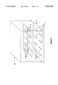
- FIG. 1 contains and illustration of how certain of the modules of the present invention are assembled and shows the principle or placing the back-contact PV cells over an array of electrical conductors.
- FIG. 2 shows resistance data for various materials tested for use in the modules of the claimed invention.
- FIG. 3 illustrates the arrangement of PV module components in one embodiment of the invention.
- FIG. 4 illustrates the arrangement of PV module components in another embodiment of the invention.
- New module concepts are disclosed here which use back-contact c-Si solar cells such as the ones described in the Gee, U.S. Pat. No. 5,468,652, mentioned above.
- the principles of the invention would apply equally as well to any solar cells bearing electrical contacts on a single side rather than on two sides.
- current commercial PV modules are typically manufactured using solar cells with contacts both on the front and back surfaces of the photovoltaic substrate.
- Significant cost savings and improvements in module assembly throughput can be achieved with module concepts that encapsulate and electrically connect all the cells in the module in a single step.
- the new modules claimed here incorporate the following features: (1) back-contact cells, (2) a module backplane that has both the electrical circuit and the encapsulation/backsheet in a single piece, and (3) a single-step process for assembly of these components into a module.
- These features result in cost savings because of the reduced number of steps needed in manufacturing, elimination of low-throughput steps such as individual cell tabbing and cell stringing, and easy automation due to utilization of completely planar processes.
- These planar processes are referred to here collectively as “monolithic module assembly”, and the modules manufactured according to these processes are referred to as “monolithic modules”, since they translate many of the advantages of monolithic module construction of thin-film PV to wafered c-Si PV.
- Simplifications in module fabrication may reduce cost of module fabrication by up to 50% which corresponds to a reduction of around 25% in the total manufacturing cost for a module.
- cost reduction estimates for a space PV array using back-contact solar cells see G. J. Pack and J. A. Mann, 16 th IEEE Photovoltaic Specialists Conference, 36-38, 1982.
- FIG. 1 shows schematically how the various elements within the invention "monolithic module” are assembled.
- electrically conductive circuit elements 7 are prepatterned (or placed) onto the surface of a backsheet 5. The pattern is selected based on the electrical requirements of the module to be manufactured and in part dictated by the dimensions of the solar cells to be used on the module. Specifically, the electrical circuit elements (or conductors) are positioned so that when they connected by solar cells, an electric circuit capable of generating power is created. The decisions about how precisely to configure the electrical circuit and where exactly to locate the electrically conductive circuit elements 7 relative to each other are within the capabilities of skilled practitioners in the art of PV module constriction.
- Back-contact solar cells 10 are then positioned atop the electrically conductive circuit elements 7 so that the contacts of the solar cells complete the circuit.
- the advantage of prepositioning the electrical conductors and then placing solar cells in contact with the conductors is that this enables all of the electrical conductors to be arranged on a module or section of a module in one step and all of the solar cells likewise to be positioned in one step. This represents significant potential cost savings over sequentially soldering solar cells and connector tabs in series or in parallel to create a desired electrical circuit.
- a sheet of polymer encapsulation material (not shown in the figure) is then positioned over the surfaces of the solar cells 10 and the backsheet 5, and finally a cover 15 of glass is placed atop the assembled elements.
- materials other than glass may serve the objectives and purposes of those manufacturing given modules. Although glass is used in the best mode, such other materials are contemplated by this invention and are intended to fall within the scope of the claims.
- the module is then sealed using heat and pressure or another sealing method suited to the particular polymer encapsulation material selected. In the best mode demonstrated by the inventors, vacuum pressure laminators common in the field of PV module construction are used, however, other lamination technologies such as rollbased laminators can be adapted to manufacture the modules of the claimed invention.
- FIG. 2 shows on a graph data on the resistance of the different interconnect technologies examined and evaluated for use in this invention. Comparisons were made of resistance between copper tabs and a solar-cell silver for silver-loaded epoxy, Pb:Sn solder, two types of pressure-sensitive conductive adhesives (PSA) and thermosetting conductive adhesive (TSA). Several samples of each type were measured. All the interconnects met the target resistance of less than 1 m ⁇ cm 2 . None of the materials could achieve a resistance as low as Pb:Sn solder, and soldering represents a viable option for electrically connecting the cells to the traces in the monolithic module as it achieves good wetting of surfaces during encapsulation. Because of the need to ensure compatibility of materials, though, other options are considered as well.
- the conductive adhesives were satisfactory from the standpoint of cost and are believed to be more compatible with the encapsulation materials and process than the other interconnect options.
- the pressure-sensitive adhesives tested by the inventors showed some promise, yet reproducibility and reliability of results were not as favorable as some of the other technologies. Based on these considerations, copper foil coated with a thermosetting conductive adhesive containing silver particles is considered to be the best interconnect alternative.
- Other conductive adhesives or epoxies, though, with or without metal particles, may be used and are considered to fall within the scope of the claims. Additionally, favorable results can be obtained when the conductive circuit elements are coated with tin.
- FIGS. 3 and 4 Two different module configurations are shown in FIGS. 3 and 4.
- electrically conductive circuit elements 7 are positioned on a backsheet 5.
- the backsheet 5 should be made of material which is capable both of providing positional accuracy of the circuit elements and protecting the completed module to it from deleterious environmental elements to which the module is likely to be exposed.
- the circuit elements are, for example, strips of electrically conductive foil arranged so that when back-contact solar cells 10 are placed on them the circuit is completed.
- the solar cells are positioned so that the terminals 13 on the cells (corresponding to the p-type and n-type current collection grids of the cells) are in electrical contact with the electrically conductive circuit elements 7.
- the figure also shows the circuit elements to be coated with a conductive adhesive 17 which serves both to enhance the electrical conduction between the electrically conductive circuit elements 7 and the cell terminals 13 and to provide some degree of physical stabilization to these components during the remainder of the assembly process.
- a conductive adhesive 17 which serves both to enhance the electrical conduction between the electrically conductive circuit elements 7 and the cell terminals 13 and to provide some degree of physical stabilization to these components during the remainder of the assembly process.
- Various conductive adhesives be used for this purpose, as indicated in the discussion above pertaining to FIG. 2.
- a sheet of encapsulant material 25 capable of flowing upon application of heat and pressure is positioned over the cells, and finally, a sheet of transparent protective material 15 (such as glass) is positioned over the sheet of encapsulant material 25.
- a sheet of transparent protective material 15 such as glass
- the sequence of placement of the elements described can be altered or reversed without departing from the spirit of the invention.
- the glass can be positioned first, followed by the encapsulant, cells and backsheet (with electrically conductive circuit elements attached).
- the assembly is laminated using application of heat and pressure by any of a variety of photovoltaic module lamination processes known to those skilled in the art of photovoltaic module manufacture. Examples include use of a vacuum pressure laminator or roll-based laminator.
- the electrically conductive circuit elements 7 when they are initially arranged on the backsheet 5, they need to be positioned so that, after the solar cells 10 are placed on them, gaps 22 are left between the surfaces of the solar cells. These gaps accommodate thermal expansion of the cells both during the lamination procedure and in a completed module exposed to sunlight. They also allow encapsulant material to flow between the cells and into the interstices surrounding the module components during the lamination process, thereby allowing the encapsulant to provide physical support to the components in the finished module.
- a photovoltaic module which, in the simplest case needed in order to be functional, includes a planar member having two sides, an array of electrical conductors affixed to one side of the planar member, a plurality of back-contact solar cells bearing electrical terminals overlaying the array of electrical conductors with the electrical terminals in electrical contact with the electrical conductors thereby creating an electrical circuit capable of generating power, and encapsulation material in physical contact with the back-contact solar cells.
- a sheet of glass or, in theory, other durable transparent material is included to shield the electrical components of the module from environmental hazards.
- FIG. 4 a slightly more complex module is illustrated.
- a planar piece of mesh 4 (made, for example, of a polymer material) is used as the surface on which electrically conductive circuit elements 7 are positioned.
- considerations regarding the placement of the conductive circuit elements are similar to those mentioned above in the discussion of FIG. 3.
- solar cells are positioned so that the terminals 13 on the cells are in electrical contact with the electrically conductive circuit elements 7.
- the figure shows the circuit elements coated with a conductive adhesive 17.
- the preferred encapsulant material is ethylene vinyl acetate (EVA) which is a commonly used encapsulant material in the photovoltaic industry.
- FIG. 4 also illustrates use of a protective backsheet 6 positioned beyond the encapsulant material on the side of the planar mesh 4 away from the electrically conductive circuit elements 7 and solar cells 10.
- the purpose of this backsheet 6 is to provide protection against the environmental elements.
- a typical backsheet material such as TedlarTM, commonly used in the commercial photovoltaic industry, is suitable for this purpose. Protection for the front side of the solar cells, as in the previous embodiment, is provided by placing a sheet of glass or other appropriate transparent protective material 15 over the sheet of encapsulant material adjacent to the surfaces of the cells 10.
- the assembly is laminated using application of heat and pressure by photovoltaic module lamination processes known in the industry.
- the reason for using a planar piece of mesh 4 in this embodiment to support the circuit is to allow the encapsulant material to flow through openings in the mesh, as well as around the cells 10 and electrically conductive circuit elements 7 to allow a full encapsulation which helps to seal the protective backsheet 6 to the back side of the module an the sheet of transparent protective material 15 to the front side of the module.
- the cells 10 need to be positioned such that gaps 22 are left between them though which encapsulant can flow upon application of heat and pressure.
- the result in this embodiment is a photovoltaic module which, in the simplest case needed in order to be functional, includes a planar structural support comprising a mesh and having two sides, an array of electrical conductors affixed to one side of the planar structural support, back-contact crystalline silicon solar cells bearing electrical terminals overlaying the array of electrical conductors with the electrical terminals in electrical contact with the electrical conductors and creating an electrical circuit capable of generating power is created, a sheet of glass overlaying the back-contact crystalline silicon solar cells, a protective backsheet covering the planar structural support on the side opposite the side to which the array of electrical conductors is affixed, and encapsulation material in physical contact with the back-contact crystalline silicon solar cells and between the protective backsheet and the sheet of glass.
Abstract
Description
Claims (21)
Priority Applications (1)
| Application Number | Priority Date | Filing Date | Title |
|---|---|---|---|
| US08/994,071 US5951786A (en) | 1997-12-19 | 1997-12-19 | Laminated photovoltaic modules using back-contact solar cells |
Applications Claiming Priority (1)
| Application Number | Priority Date | Filing Date | Title |
|---|---|---|---|
| US08/994,071 US5951786A (en) | 1997-12-19 | 1997-12-19 | Laminated photovoltaic modules using back-contact solar cells |
Publications (1)
| Publication Number | Publication Date |
|---|---|
| US5951786A true US5951786A (en) | 1999-09-14 |
Family
ID=25540256
Family Applications (1)
| Application Number | Title | Priority Date | Filing Date |
|---|---|---|---|
| US08/994,071 Expired - Lifetime US5951786A (en) | 1997-12-19 | 1997-12-19 | Laminated photovoltaic modules using back-contact solar cells |
Country Status (1)
| Country | Link |
|---|---|
| US (1) | US5951786A (en) |
Cited By (116)
| Publication number | Priority date | Publication date | Assignee | Title |
|---|---|---|---|---|
| US6294725B1 (en) * | 2000-03-31 | 2001-09-25 | Trw Inc. | Wireless solar cell array electrical interconnection scheme |
| US20020153038A1 (en) * | 2001-04-20 | 2002-10-24 | Akimasa Umemoto | Photovoltaic module having light receptive, glass laminate structure and photovoltaic module having light receptive, multi-layer structure |
| DE10141276A1 (en) * | 2001-08-23 | 2003-03-13 | Astrium Gmbh | Solar module has wraparound cells electrically connected by elastic contact bridges between wraparound cells and base plate and permanently pressed onto contact surfaces of adjacent wraparound cells |
| US20030127124A1 (en) * | 2002-01-04 | 2003-07-10 | Jones Bernard D. | Solar cell stringing machine |
| FR2853993A1 (en) * | 2003-04-16 | 2004-10-22 | Dgtec | Production of a photovoltaic module with photovoltaic cells arranged between glass substrates and incorporating a sealing joint enclosing the volume containing the cells |
| US20040261840A1 (en) * | 2003-06-30 | 2004-12-30 | Advent Solar, Inc. | Emitter wrap-through back contact solar cells on thin silicon wafers |
| US20050172996A1 (en) * | 2004-02-05 | 2005-08-11 | Advent Solar, Inc. | Contact fabrication of emitter wrap-through back contact silicon solar cells |
| US20050172998A1 (en) * | 2004-02-05 | 2005-08-11 | Advent Solar, Inc. | Buried-contact solar cells with self-doping contacts |
| US20050176164A1 (en) * | 2004-02-05 | 2005-08-11 | Advent Solar, Inc. | Back-contact solar cells and methods for fabrication |
| DE102004010115A1 (en) * | 2004-02-27 | 2005-09-29 | Bayerisches Zentrum für angewandte Energieforschung eV, ZAE Bayern | Semiconductor circuit manufacturing method, involves bonding discrete semiconductor components on substrate such that base and emitter terminals of corresponding P and N conductive regions on one side of substrate are accessible |
| US20060042681A1 (en) * | 2004-08-24 | 2006-03-02 | General Electric Company | Pv laminate backplane with optical concentrator |
| US20060060238A1 (en) * | 2004-02-05 | 2006-03-23 | Advent Solar, Inc. | Process and fabrication methods for emitter wrap through back contact solar cells |
| US20060157103A1 (en) * | 2005-01-20 | 2006-07-20 | Nanosolar, Inc. | Optoelectronic architecture having compound conducting substrate cross-reference to related application |
| US20060162766A1 (en) * | 2003-06-26 | 2006-07-27 | Advent Solar, Inc. | Back-contacted solar cells with integral conductive vias and method of making |
| US20060180195A1 (en) * | 1999-03-30 | 2006-08-17 | Daniel Luch | Substrate and collector grid structures for integrated photovoltaic arrays and process of manufacture of such arrays |
| US20060272699A1 (en) * | 2003-04-16 | 2006-12-07 | Apollon Solar | Photovoltaic module and method for production thereof |
| US7244888B1 (en) * | 2001-06-22 | 2007-07-17 | Kunihide Tanaka | Solar energy converter using a solar cell in a shallow liquid-gel layer |
| US20080143601A1 (en) * | 2006-11-30 | 2008-06-19 | Tenxc Wireless Inc. | Butler matrix implementation |
| US20080185033A1 (en) * | 2007-02-06 | 2008-08-07 | Kalejs Juris P | Solar electric module |
| US20080227236A1 (en) * | 1995-05-15 | 2008-09-18 | Daniel Luch | Substrate structures for integrated series connected photovoltaic arrays and process of manufacture of such arrays |
| US20080236655A1 (en) * | 2007-03-29 | 2008-10-02 | Baldwin Daniel F | Solar module manufacturing processes |
| WO2008141878A1 (en) * | 2007-05-24 | 2008-11-27 | International Business Machines Corporation | Method of contacting photovoltaic modules |
| US20080314433A1 (en) * | 1995-05-15 | 2008-12-25 | Daniel Luch | Substrate structures for integrated series connected photovoltaic arrays and process of manufacture of such arrays |
| US20090032087A1 (en) * | 2007-02-06 | 2009-02-05 | Kalejs Juris P | Manufacturing processes for light concentrating solar module |
| US20090101204A1 (en) * | 2007-10-22 | 2009-04-23 | Biosolar, Inc. | Photovoltaic laminated module backsheet, films and coatings for use in module backsheet, and processes for making the same |
| US20090126786A1 (en) * | 2007-11-13 | 2009-05-21 | Advent Solar, Inc. | Selective Emitter and Texture Processes for Back Contact Solar Cells |
| US20090178704A1 (en) * | 2007-02-06 | 2009-07-16 | Kalejs Juris P | Solar electric module with redirection of incident light |
| EP2109150A1 (en) * | 2007-01-31 | 2009-10-14 | Sharp Kabushiki Kaisha | Solar cell module, wiring member for solar cell, and method for manufacturing solar cell module |
| US20090288697A1 (en) * | 2006-08-29 | 2009-11-26 | Hitachi Chemical Co., Ltd. | Conductive adhesive film and solar cell module |
| US20090308447A1 (en) * | 2006-05-10 | 2009-12-17 | Sitec Meldetechnik Gmbh | Photovoltaic module with at least one crystalline solar cell |
| US20100012172A1 (en) * | 2008-04-29 | 2010-01-21 | Advent Solar, Inc. | Photovoltaic Modules Manufactured Using Monolithic Module Assembly Techniques |
| US20100108141A1 (en) * | 2007-05-09 | 2010-05-06 | Hitachi Chemical Company, Ltd. | Method for connecting conductor, member for connecting conductor, connecting structure and solar cell module |
| US20100116314A1 (en) * | 2007-05-09 | 2010-05-13 | Hitachi Chemical Company, Ltd. | Conductor connection member, connection structure, and solar cell module |
| WO2010082594A1 (en) | 2009-01-16 | 2010-07-22 | シャープ株式会社 | Solar cell module and method for manufacturing solar cell module |
| US20100200058A1 (en) * | 2007-09-28 | 2010-08-12 | Yasushi Funakoshi | Solar battery, method for manufacturing solar battery, method for manufacturing solar cell module, and solar cell module |
| US20100206352A1 (en) * | 2009-02-13 | 2010-08-19 | Applied Materials, Inc. | Low-concentration flat profile photovoltaic modules |
| US20100229917A1 (en) * | 2009-03-11 | 2010-09-16 | Chulchae Choi | Solar cell and solar cell module |
| WO2010110083A1 (en) | 2009-03-25 | 2010-09-30 | シャープ株式会社 | Back electrode type solar cell, wiring sheet, solar cell provided with wiring sheet, solar cell module, method for manufacturing solar cell provided with wiring sheet, and method for manufacturing solar cell module |
| WO2010116973A1 (en) | 2009-04-08 | 2010-10-14 | シャープ株式会社 | Interconnect sheet, solar cell with interconnect sheet, solar module, and method of producing solar cell with interconnect sheet |
| US20100263718A1 (en) * | 2007-11-09 | 2010-10-21 | Yoshiya Abiko | Solar cell module and method for manufacturing solar cell module |
| WO2010087712A3 (en) * | 2009-01-30 | 2010-11-25 | Renewable Energy Corporation Asa | Back contacting and interconnection of two solar cells |
| WO2010136162A2 (en) * | 2009-05-26 | 2010-12-02 | Fraunhofer-Gesellschaft zur Förderung der angewandten Forschung e.V. | Method for producing a solar module |
| WO2010139454A2 (en) * | 2009-06-04 | 2010-12-09 | Fraunhofer-Gesellschaft zur Förderung der angewandten Forschung e.V. | Photovoltaic module having a planar cell connector |
| US7851700B2 (en) | 1999-03-30 | 2010-12-14 | Daniel Luch | Substrate and collector grid structures for integrated series connected photovoltaic arrays and process of manufacture of such arrays |
| WO2011001883A1 (en) | 2009-06-29 | 2011-01-06 | シャープ株式会社 | Wiring sheet, solar cell with wiring sheet, solar cell module and wiring sheet roll |
| US20110017281A1 (en) * | 2008-03-17 | 2011-01-27 | Yasushi Funakoshi | Solar cell module and method for manufacturing solar cell module |
| JP2011035070A (en) * | 2009-07-30 | 2011-02-17 | Toppan Printing Co Ltd | Back sheet for solar cell module, and method of manufacturing the same |
| US7898053B2 (en) | 2000-02-04 | 2011-03-01 | Daniel Luch | Substrate structures for integrated series connected photovoltaic arrays and process of manufacture of such arrays |
| US7898054B2 (en) | 2000-02-04 | 2011-03-01 | Daniel Luch | Substrate structures for integrated series connected photovoltaic arrays and process of manufacture of such arrays |
| JP2011054721A (en) * | 2009-09-01 | 2011-03-17 | Sharp Corp | Bonding method of bonded member, and bonding structure |
| WO2011003969A3 (en) * | 2009-07-10 | 2011-04-21 | Eppsteinfoils Gmbh & Co Kg | Composite system for photovoltaic modules |
| EP2330635A1 (en) | 2009-12-02 | 2011-06-08 | Esmolo AG | Interconnection Device |
| US20110155225A1 (en) * | 2009-08-21 | 2011-06-30 | Applied Materials, Inc. | Back contact solar cells having exposed vias |
| US20110155203A1 (en) * | 2007-08-07 | 2011-06-30 | Yasushi Funakoshi | Solar cell module |
| US8076568B2 (en) | 2006-04-13 | 2011-12-13 | Daniel Luch | Collector grid and interconnect structures for photovoltaic arrays and modules |
| US8110737B2 (en) | 1999-03-30 | 2012-02-07 | Daniel Luch | Collector grid, electrode structures and interrconnect structures for photovoltaic arrays and methods of manufacture |
| EP2416385A1 (en) * | 2010-08-02 | 2012-02-08 | Scheuten S.à.r.l. | Multi-layer back contact film |
| US8138413B2 (en) | 2006-04-13 | 2012-03-20 | Daniel Luch | Collector grid and interconnect structures for photovoltaic arrays and modules |
| DE102010016976A1 (en) | 2010-05-17 | 2012-03-22 | Schott Solar Ag | Method for interconnecting solar cells, involves assigning back contact solar cells on second and third electric guards to contact back led front face region according to back contact solar cells in series which are interconnected |
| EP2439781A1 (en) * | 2009-06-03 | 2012-04-11 | Sony Chemical & Information Device Corporation | Method for manufacturing solar cell modules |
| US8198117B2 (en) | 2005-08-16 | 2012-06-12 | Nanosolar, Inc. | Photovoltaic devices with conductive barrier layers and foil substrates |
| US8198696B2 (en) | 2000-02-04 | 2012-06-12 | Daniel Luch | Substrate structures for integrated series connected photovoltaic arrays and process of manufacture of such arrays |
| US20120176077A1 (en) * | 2011-01-07 | 2012-07-12 | Samsung Electro-Mechanics Co., Ltd. | Solar cell module having white back sheet |
| US8222513B2 (en) | 2006-04-13 | 2012-07-17 | Daniel Luch | Collector grid, electrode structures and interconnect structures for photovoltaic arrays and methods of manufacture |
| CN102623573A (en) * | 2012-04-16 | 2012-08-01 | 英利能源(中国)有限公司 | Connection method for terminal box of solar back contact battery pack and solar battery pack |
| US8247243B2 (en) | 2009-05-22 | 2012-08-21 | Nanosolar, Inc. | Solar cell interconnection |
| WO2012125587A1 (en) | 2011-03-11 | 2012-09-20 | Avery Dennison Corporation | Sheet assembly with aluminum based electrodes |
| DE102011055754A1 (en) | 2011-06-01 | 2012-12-06 | Schott Solar Ag | Solar cell module and method for interconnecting solar cells |
| US20130037527A1 (en) * | 2011-08-08 | 2013-02-14 | Applied Materials, Inc. | Fixture for Drilling Vias in Back-Contact Solar Cells |
| EP2561553A2 (en) * | 2010-04-20 | 2013-02-27 | Robert Bosch GmbH | Method for producing a photovoltaic module having semiconductor cells connected on the back side, and photovoltaic module |
| CN103035763A (en) * | 2011-09-29 | 2013-04-10 | Lg电子株式会社 | Solar cell module |
| KR101284278B1 (en) * | 2011-04-12 | 2013-07-08 | 엘지전자 주식회사 | Solar cell module and interconnector used in solar cell module |
| WO2013116876A2 (en) | 2012-02-03 | 2013-08-08 | Avery Dennison Corporation | Sheet assembly with aluminum based electrodes |
| WO2013115851A1 (en) | 2012-02-03 | 2013-08-08 | Avery Dennison Corporation | Laser patterning of photovoltaic backsheet |
| JP2014504040A (en) * | 2011-01-26 | 2014-02-13 | スパイア・コーポレーション | Photovoltaic module and method |
| US8664030B2 (en) | 1999-03-30 | 2014-03-04 | Daniel Luch | Collector grid and interconnect structures for photovoltaic arrays and modules |
| US20140083503A1 (en) * | 2012-09-27 | 2014-03-27 | Win Win Precision Technology Co., Ltd. | Solar cell module and manufacturing method thereof |
| US20140116500A1 (en) * | 2012-10-31 | 2014-05-01 | Emcore Solar Power, Inc. | Inverted metamorphic multijunction solar cells mounted on flexible support with bifacial contacts |
| US8729385B2 (en) | 2006-04-13 | 2014-05-20 | Daniel Luch | Collector grid and interconnect structures for photovoltaic arrays and modules |
| US20140190546A1 (en) * | 2011-08-31 | 2014-07-10 | Sanyo Electric Co., Ltd. | Solar module and solar module manufacturing method |
| US8822810B2 (en) | 2006-04-13 | 2014-09-02 | Daniel Luch | Collector grid and interconnect structures for photovoltaic arrays and modules |
| US8884155B2 (en) | 2006-04-13 | 2014-11-11 | Daniel Luch | Collector grid and interconnect structures for photovoltaic arrays and modules |
| US8906803B2 (en) | 2013-03-15 | 2014-12-09 | Sandia Corporation | Method of forming through substrate vias (TSVs) and singulating and releasing die having the TSVs from a mechanical support substrate |
| US8927315B1 (en) | 2005-01-20 | 2015-01-06 | Aeris Capital Sustainable Ip Ltd. | High-throughput assembly of series interconnected solar cells |
| US20150040961A1 (en) * | 2012-04-23 | 2015-02-12 | Sanyo Electric Co., Ltd. | Solar cell module |
| US9006563B2 (en) | 2006-04-13 | 2015-04-14 | Solannex, Inc. | Collector grid and interconnect structures for photovoltaic arrays and modules |
| US9029239B2 (en) | 2007-11-01 | 2015-05-12 | Sandia Corporation | Separating semiconductor devices from substrate by etching graded composition release layer disposed between semiconductor devices and substrate including forming protuberances that reduce stiction |
| TWI492392B (en) * | 2010-08-27 | 2015-07-11 | Ind Tech Res Inst | Semiconductor device module package structure and series connection method thereof |
| US9236512B2 (en) | 2006-04-13 | 2016-01-12 | Daniel Luch | Collector grid and interconnect structures for photovoltaic arrays and modules |
| US9666739B2 (en) | 2013-06-28 | 2017-05-30 | Sunpower Corporation | Photovoltaic cell and laminate metallization |
| US20170162737A1 (en) * | 2015-12-02 | 2017-06-08 | Solarworld Innovations Gmbh | Bifacial photovoltaic module |
| US9708509B2 (en) | 2012-10-09 | 2017-07-18 | Avery Dennison Corporation | Adhesives and related methods |
| US9722115B2 (en) | 2012-12-26 | 2017-08-01 | Industrial Technology Research Institute | Solar cell encapsulating module and method for manufacturing the same |
| US9865758B2 (en) | 2006-04-13 | 2018-01-09 | Daniel Luch | Collector grid and interconnect structures for photovoltaic arrays and modules |
| US10526511B2 (en) | 2016-12-22 | 2020-01-07 | Avery Dennison Corporation | Convertible pressure sensitive adhesives comprising urethane (meth)acrylate oligomers |
| US10535785B2 (en) | 2014-12-19 | 2020-01-14 | Sunpower Corporation | Laser beam shaping for foil-based metallization of solar cells |
| US10566474B2 (en) | 2013-12-20 | 2020-02-18 | Sunpower Corporation | Single-step metal bond and contact formation for solar cells |
| US10593825B2 (en) | 2016-05-13 | 2020-03-17 | Sunpower Corporation | Roll-to-roll metallization of solar cells |
| US10615296B2 (en) | 2014-03-28 | 2020-04-07 | Sunpower Corporation | Foil-based metallization of solar cells |
| US10672924B2 (en) | 2015-10-29 | 2020-06-02 | Sunpower Corporation | Laser foil trim approaches for foil-based metallization for solar cells |
| US10700222B2 (en) | 2014-03-28 | 2020-06-30 | Sunpower Corporation | Metallization of solar cells |
| US10727369B2 (en) | 2016-09-30 | 2020-07-28 | Sunpower Corporation | Conductive foil based metallization of solar cells |
| US10879413B2 (en) | 2013-12-20 | 2020-12-29 | Sunpower Corporation | Contacts for solar cells |
| US10930804B2 (en) | 2013-09-27 | 2021-02-23 | Sunpower Corporation | Metallization of solar cells using metal foils |
| US10971638B2 (en) | 2016-07-01 | 2021-04-06 | Sunpower Corporation | Laser techniques for foil-based metallization of solar cells |
| US11049421B2 (en) | 2015-02-05 | 2021-06-29 | Avery Dennison Corporation | Label assemblies for adverse environments |
| US11063160B2 (en) * | 2017-03-03 | 2021-07-13 | Kaneka Corporation | Solar cell module |
| US11276785B2 (en) | 2018-04-06 | 2022-03-15 | Sunpower Corporation | Laser assisted metallization process for solar cell fabrication |
| US11362220B2 (en) | 2018-04-06 | 2022-06-14 | Sunpower Corporation | Local metallization for semiconductor substrates using a laser beam |
| US11362234B2 (en) | 2018-04-06 | 2022-06-14 | Sunpower Corporation | Local patterning and metallization of semiconductor structures using a laser beam |
| US11424373B2 (en) | 2016-04-01 | 2022-08-23 | Sunpower Corporation | Thermocompression bonding approaches for foil-based metallization of non-metal surfaces of solar cells |
| US11646387B2 (en) | 2018-04-06 | 2023-05-09 | Maxeon Solar Pte. Ltd. | Laser assisted metallization process for solar cell circuit formation |
| US11664472B2 (en) | 2018-04-06 | 2023-05-30 | Maxeon Solar Pte. Ltd. | Laser assisted metallization process for solar cell stringing |
| US11894472B2 (en) | 2015-06-26 | 2024-02-06 | Maxeon Solar Pte. Ltd. | Leave-in etch mask for foil-based metallization of solar cells |
| US11908958B2 (en) | 2016-12-30 | 2024-02-20 | Maxeon Solar Pte. Ltd. | Metallization structures for solar cells |
| US11939688B2 (en) | 2019-03-29 | 2024-03-26 | California Institute Of Technology | Apparatus and systems for incorporating effective transparent catalyst for photoelectrochemical application |
Citations (2)
| Publication number | Priority date | Publication date | Assignee | Title |
|---|---|---|---|---|
| US5468652A (en) * | 1993-07-14 | 1995-11-21 | Sandia Corporation | Method of making a back contacted solar cell |
| US5797998A (en) * | 1994-03-31 | 1998-08-25 | Pacific Solar Pty. Limited | Multiple layer thin film solar cells with buried contacts |
-
1997
- 1997-12-19 US US08/994,071 patent/US5951786A/en not_active Expired - Lifetime
Patent Citations (2)
| Publication number | Priority date | Publication date | Assignee | Title |
|---|---|---|---|---|
| US5468652A (en) * | 1993-07-14 | 1995-11-21 | Sandia Corporation | Method of making a back contacted solar cell |
| US5797998A (en) * | 1994-03-31 | 1998-08-25 | Pacific Solar Pty. Limited | Multiple layer thin film solar cells with buried contacts |
Non-Patent Citations (20)
| Title |
|---|
| A. Sch o necker, H. H. C. De Moor, A. R. Burgers, A. W. Weeber, J. Hoomstra, W. C. Sinke, P.P. Michiels, R. A. Steeman, An Industrial Multi Crystalline EWT Solar Cell with Screen Printed Matallisation, 14 th European Photovoltaic Solar Energy Conference and Exhibition (ECPVSEC), Barcelona, Spain, Jun./Jul. 1997. * |
| A. Schonecker, H. H. C. De Moor, A. R. Burgers, A. W. Weeber, J. Hoomstra, W. C. Sinke, P.P. Michiels, R. A. Steeman, An Industrial Multi-Crystalline EWT Solar Cell with Screen Printed Matallisation, 14th European Photovoltaic Solar Energy Conference and Exhibition (ECPVSEC), Barcelona, Spain, Jun./Jul. 1997. |
| David Thorp, Methods of Contacting Multijunction Silicon Photovoltaic Modules , 14 th ECPVSEC, Barcelona, Spain Jun./Jul. 1997. * |
| David Thorp,Methods of Contacting Multijunction Silicon Photovoltaic Modules, 14th ECPVSEC, Barcelona, Spain Jun./Jul. 1997. |
| Frank R. Jeffrey, Derrick P. Grimmer, Steven Brayman, Bradley Scandrett, Michael Thomas, Steven A. Martens, Wei Chen, and Max Noak, PVMaT Improvements in Monolithic a Si Modules on Continuous Polymer Substrates , CP394, NREL/SNL Photovoltaics Program Review, AIP Press, New York, 1997, pp. 451 461. * |
| Frank R. Jeffrey, Derrick P. Grimmer, Steven Brayman, Bradley Scandrett, Michael Thomas, Steven A. Martens, Wei Chen, and Max Noak, PVMaT Improvements in Monolithic a-Si Modules on Continuous Polymer Substrates, CP394, NREL/SNL Photovoltaics Program Review, AIP Press, New York, 1997, pp. 451-461. |
| G. J. Pack and J. A. Mann, New Component Development for Multi 100kW Low Cost Solar Array Applications, IEEE, 1982. * |
| G. J. Pack and J. A. Mann, New Component Development for Multi-100kW Low-Cost Solar Array Applications, IEEE, 1982. |
| J. I. Hanoka, P. M. Kane, R. G. Chleboski, and M. A. Farber, Advanced Polymer PV System , CP394, NREL/SNL Photvoltaics Program Review, AIP Press, New York, 1997, pp. 859 866. * |
| J. I. Hanoka, P. M. Kane, R. G. Chleboski, and M. A. Farber, Advanced Polymer PV System, CP394, NREL/SNL Photvoltaics Program Review, AIP Press, New York, 1997, pp. 859-866. |
| James M. Gee, M. E. Buck, W. Kent Schubert, and Paul A. Basore, Progress on the Emitter Wrap Through Silicon Solar Cell, 12 th European Community Photovoltaic Solar Energy Conference, Amsterdam, The Netherlands, Apr. 1994. * |
| James M. Gee, M. E. Buck, W. Kent Schubert, and Paul A. Basore, Progress on the Emitter Wrap-Through Silicon Solar Cell, 12th European Community Photovoltaic Solar Energy Conference, Amsterdam, The Netherlands, Apr. 1994. |
| James M. Gee, W. Kent Schuvert, and Paul A. Basore, Emitter Wrap Through Solar Cell, 23 rd IEEE Photovoltaic Specialists Conference, Louisville, KY, May 1993. * |
| James M. Gee, W. Kent Schuvert, and Paul A. Basore, Emitter Wrap-Through Solar Cell, 23rd IEEE Photovoltaic Specialists Conference, Louisville, KY, May 1993. |
| Kim W. Mitchell, Richard R. King, Theresa L. Jester, and Michael McGraw, The Reformation of Cz Si Photovoltaics, First WCPEC; Dec. 5 9, 1994; Hawaii, IEEE 1994. * |
| Kim W. Mitchell, Richard R. King, Theresa L. Jester, and Michael McGraw, The Reformation of Cz Si Photovoltaics, First WCPEC; Dec. 5-9, 1994; Hawaii, IEEE 1994. |
| Michael Kardauskas, Juris Kalejs, Jeff Cao, Eric tornstrom, Ronald Goniorawski, Colleen O Brien, and Mert Prince, Market Driven Improvements in the Manufacturing of EFG Modules , CP394, NREL/SNL Photovoltaics Program Review, AIP Press, New York, 1997, pp. 851 585. * |
| Michael Kardauskas, Juris Kalejs, Jeff Cao, Eric tornstrom, Ronald Goniorawski, Colleen O'Brien, and Mert Prince, Market-Driven Improvements in the Manufacturing of EFG Modules, CP394, NREL/SNL Photovoltaics Program Review, AIP Press, New York, 1997, pp. 851-585. |
| S. R. Wenham, M. A. Green, M. E. Watt, Applied Photovoltaics , Chapter 5, Centre for Photovoltaic Devices and Systems, University of South Wales, 1995. * |
| S. R. Wenham, M. A. Green, M. E. Watt, Applied Photovoltaics, Chapter 5, Centre for Photovoltaic Devices and Systems, University of South Wales, 1995. |
Cited By (195)
| Publication number | Priority date | Publication date | Assignee | Title |
|---|---|---|---|---|
| US7732243B2 (en) | 1995-05-15 | 2010-06-08 | Daniel Luch | Substrate structures for integrated series connected photovoltaic arrays and process of manufacture of such arrays |
| US20080314433A1 (en) * | 1995-05-15 | 2008-12-25 | Daniel Luch | Substrate structures for integrated series connected photovoltaic arrays and process of manufacture of such arrays |
| US20080227236A1 (en) * | 1995-05-15 | 2008-09-18 | Daniel Luch | Substrate structures for integrated series connected photovoltaic arrays and process of manufacture of such arrays |
| US8110737B2 (en) | 1999-03-30 | 2012-02-07 | Daniel Luch | Collector grid, electrode structures and interrconnect structures for photovoltaic arrays and methods of manufacture |
| US8664030B2 (en) | 1999-03-30 | 2014-03-04 | Daniel Luch | Collector grid and interconnect structures for photovoltaic arrays and modules |
| US8319097B2 (en) | 1999-03-30 | 2012-11-27 | Daniel Luch | Substrate and collector grid structures for integrated series connected photovoltaic arrays and process of manufacture of such arrays |
| US8304646B2 (en) | 1999-03-30 | 2012-11-06 | Daniel Luch | Substrate and collector grid structures for integrated series connected photovoltaic arrays and process of manufacture of such arrays |
| US7851700B2 (en) | 1999-03-30 | 2010-12-14 | Daniel Luch | Substrate and collector grid structures for integrated series connected photovoltaic arrays and process of manufacture of such arrays |
| US7868249B2 (en) | 1999-03-30 | 2011-01-11 | Daniel Luch | Substrate and collector grid structures for integrated series connected photovoltaic arrays and process of manufacture of such arrays |
| US7989693B2 (en) | 1999-03-30 | 2011-08-02 | Daniel Luch | Substrate and collector grid structures for integrated series connected photovoltaic arrays and process of manufacture of such arrays |
| US7635810B2 (en) | 1999-03-30 | 2009-12-22 | Daniel Luch | Substrate and collector grid structures for integrated photovoltaic arrays and process of manufacture of such arrays |
| US20060180195A1 (en) * | 1999-03-30 | 2006-08-17 | Daniel Luch | Substrate and collector grid structures for integrated photovoltaic arrays and process of manufacture of such arrays |
| US7989692B2 (en) | 1999-03-30 | 2011-08-02 | Daniel Luch | Substrate and collector grid structures for integrated series connected photovoltaic arrays and process of manufacturing of such arrays |
| US7898054B2 (en) | 2000-02-04 | 2011-03-01 | Daniel Luch | Substrate structures for integrated series connected photovoltaic arrays and process of manufacture of such arrays |
| US7898053B2 (en) | 2000-02-04 | 2011-03-01 | Daniel Luch | Substrate structures for integrated series connected photovoltaic arrays and process of manufacture of such arrays |
| US8198696B2 (en) | 2000-02-04 | 2012-06-12 | Daniel Luch | Substrate structures for integrated series connected photovoltaic arrays and process of manufacture of such arrays |
| US6294725B1 (en) * | 2000-03-31 | 2001-09-25 | Trw Inc. | Wireless solar cell array electrical interconnection scheme |
| US20020153038A1 (en) * | 2001-04-20 | 2002-10-24 | Akimasa Umemoto | Photovoltaic module having light receptive, glass laminate structure and photovoltaic module having light receptive, multi-layer structure |
| US7202410B2 (en) * | 2001-04-20 | 2007-04-10 | Sharp Kabushiki Kaisha | Photovoltaic module having light receptive, glass laminate structure and photovoltaic module having light receptive, multi-layer structure |
| US7244888B1 (en) * | 2001-06-22 | 2007-07-17 | Kunihide Tanaka | Solar energy converter using a solar cell in a shallow liquid-gel layer |
| DE10141276A1 (en) * | 2001-08-23 | 2003-03-13 | Astrium Gmbh | Solar module has wraparound cells electrically connected by elastic contact bridges between wraparound cells and base plate and permanently pressed onto contact surfaces of adjacent wraparound cells |
| US20030127124A1 (en) * | 2002-01-04 | 2003-07-10 | Jones Bernard D. | Solar cell stringing machine |
| US6841728B2 (en) | 2002-01-04 | 2005-01-11 | G.T. Equipment Technologies, Inc. | Solar cell stringing machine |
| US20060272699A1 (en) * | 2003-04-16 | 2006-12-07 | Apollon Solar | Photovoltaic module and method for production thereof |
| FR2853993A1 (en) * | 2003-04-16 | 2004-10-22 | Dgtec | Production of a photovoltaic module with photovoltaic cells arranged between glass substrates and incorporating a sealing joint enclosing the volume containing the cells |
| US20080257401A1 (en) * | 2003-04-16 | 2008-10-23 | Apollon Solar | Photovoltaic module and method for production thereof |
| US20060162766A1 (en) * | 2003-06-26 | 2006-07-27 | Advent Solar, Inc. | Back-contacted solar cells with integral conductive vias and method of making |
| US20040261840A1 (en) * | 2003-06-30 | 2004-12-30 | Advent Solar, Inc. | Emitter wrap-through back contact solar cells on thin silicon wafers |
| US7649141B2 (en) | 2003-06-30 | 2010-01-19 | Advent Solar, Inc. | Emitter wrap-through back contact solar cells on thin silicon wafers |
| US20060060238A1 (en) * | 2004-02-05 | 2006-03-23 | Advent Solar, Inc. | Process and fabrication methods for emitter wrap through back contact solar cells |
| US20050172996A1 (en) * | 2004-02-05 | 2005-08-11 | Advent Solar, Inc. | Contact fabrication of emitter wrap-through back contact silicon solar cells |
| US7863084B2 (en) | 2004-02-05 | 2011-01-04 | Applied Materials, Inc | Contact fabrication of emitter wrap-through back contact silicon solar cells |
| US20050172998A1 (en) * | 2004-02-05 | 2005-08-11 | Advent Solar, Inc. | Buried-contact solar cells with self-doping contacts |
| US7335555B2 (en) | 2004-02-05 | 2008-02-26 | Advent Solar, Inc. | Buried-contact solar cells with self-doping contacts |
| US7144751B2 (en) | 2004-02-05 | 2006-12-05 | Advent Solar, Inc. | Back-contact solar cells and methods for fabrication |
| US20090320922A1 (en) * | 2004-02-05 | 2009-12-31 | Advent Solar, Inc. | Contact Fabrication of Emitter Wrap-Through Back Contact Silicon Solar Cells |
| US20050176164A1 (en) * | 2004-02-05 | 2005-08-11 | Advent Solar, Inc. | Back-contact solar cells and methods for fabrication |
| DE102004010115A1 (en) * | 2004-02-27 | 2005-09-29 | Bayerisches Zentrum für angewandte Energieforschung eV, ZAE Bayern | Semiconductor circuit manufacturing method, involves bonding discrete semiconductor components on substrate such that base and emitter terminals of corresponding P and N conductive regions on one side of substrate are accessible |
| US20060042681A1 (en) * | 2004-08-24 | 2006-03-02 | General Electric Company | Pv laminate backplane with optical concentrator |
| US8525152B2 (en) | 2004-09-18 | 2013-09-03 | Nanosolar, Inc. | Formation of solar cells with conductive barrier layers and foil substrates |
| US8927315B1 (en) | 2005-01-20 | 2015-01-06 | Aeris Capital Sustainable Ip Ltd. | High-throughput assembly of series interconnected solar cells |
| US7919337B2 (en) | 2005-01-20 | 2011-04-05 | Nanosolar, Inc. | Optoelectronic architecture having compound conducting substrate |
| US7968869B2 (en) | 2005-01-20 | 2011-06-28 | Nanosolar, Inc. | Optoelectronic architecture having compound conducting substrate |
| US7838868B2 (en) | 2005-01-20 | 2010-11-23 | Nanosolar, Inc. | Optoelectronic architecture having compound conducting substrate |
| US20060157103A1 (en) * | 2005-01-20 | 2006-07-20 | Nanosolar, Inc. | Optoelectronic architecture having compound conducting substrate cross-reference to related application |
| US8309949B2 (en) | 2005-01-20 | 2012-11-13 | Nanosolar, Inc. | Optoelectronic architecture having compound conducting substrate |
| US20090178706A1 (en) * | 2005-01-20 | 2009-07-16 | Sheats James R | Optoelectronic architecture having compound conducting substrate |
| US8198117B2 (en) | 2005-08-16 | 2012-06-12 | Nanosolar, Inc. | Photovoltaic devices with conductive barrier layers and foil substrates |
| US8222513B2 (en) | 2006-04-13 | 2012-07-17 | Daniel Luch | Collector grid, electrode structures and interconnect structures for photovoltaic arrays and methods of manufacture |
| US8822810B2 (en) | 2006-04-13 | 2014-09-02 | Daniel Luch | Collector grid and interconnect structures for photovoltaic arrays and modules |
| US8138413B2 (en) | 2006-04-13 | 2012-03-20 | Daniel Luch | Collector grid and interconnect structures for photovoltaic arrays and modules |
| US9006563B2 (en) | 2006-04-13 | 2015-04-14 | Solannex, Inc. | Collector grid and interconnect structures for photovoltaic arrays and modules |
| US8884155B2 (en) | 2006-04-13 | 2014-11-11 | Daniel Luch | Collector grid and interconnect structures for photovoltaic arrays and modules |
| US9865758B2 (en) | 2006-04-13 | 2018-01-09 | Daniel Luch | Collector grid and interconnect structures for photovoltaic arrays and modules |
| US9236512B2 (en) | 2006-04-13 | 2016-01-12 | Daniel Luch | Collector grid and interconnect structures for photovoltaic arrays and modules |
| US8076568B2 (en) | 2006-04-13 | 2011-12-13 | Daniel Luch | Collector grid and interconnect structures for photovoltaic arrays and modules |
| US8729385B2 (en) | 2006-04-13 | 2014-05-20 | Daniel Luch | Collector grid and interconnect structures for photovoltaic arrays and modules |
| US20090308447A1 (en) * | 2006-05-10 | 2009-12-17 | Sitec Meldetechnik Gmbh | Photovoltaic module with at least one crystalline solar cell |
| US9173302B2 (en) | 2006-08-29 | 2015-10-27 | Hitachi Chemical Company, Ltd. | Conductive adhesive film and solar cell module |
| US20090288697A1 (en) * | 2006-08-29 | 2009-11-26 | Hitachi Chemical Co., Ltd. | Conductive adhesive film and solar cell module |
| TWI456023B (en) * | 2006-08-29 | 2014-10-11 | Hitachi Chemical Co Ltd | Solar cell module manufacturing method |
| TWI456022B (en) * | 2006-08-29 | 2014-10-11 | Hitachi Chemical Co Ltd | Conductive adhesive film and solar module |
| US20080143601A1 (en) * | 2006-11-30 | 2008-06-19 | Tenxc Wireless Inc. | Butler matrix implementation |
| EP2109150A1 (en) * | 2007-01-31 | 2009-10-14 | Sharp Kabushiki Kaisha | Solar cell module, wiring member for solar cell, and method for manufacturing solar cell module |
| US20100116330A1 (en) * | 2007-01-31 | 2010-05-13 | Tetsuyoshi Inoue | Solar cell module, solar cell wiring member, and method of manufacturing solar cell module |
| EP2109150A4 (en) * | 2007-01-31 | 2011-04-06 | Sharp Kk | Solar cell module, wiring member for solar cell, and method for manufacturing solar cell module |
| US20090178704A1 (en) * | 2007-02-06 | 2009-07-16 | Kalejs Juris P | Solar electric module with redirection of incident light |
| US20090032087A1 (en) * | 2007-02-06 | 2009-02-05 | Kalejs Juris P | Manufacturing processes for light concentrating solar module |
| US20080185033A1 (en) * | 2007-02-06 | 2008-08-07 | Kalejs Juris P | Solar electric module |
| US20080236655A1 (en) * | 2007-03-29 | 2008-10-02 | Baldwin Daniel F | Solar module manufacturing processes |
| US9660131B2 (en) | 2007-05-09 | 2017-05-23 | Hitachi Chemical Company, Ltd. | Method for connecting conductor, member for connecting conductor, connecting structure and solar cell module |
| US10032952B2 (en) * | 2007-05-09 | 2018-07-24 | Hitachi Chemical Company, Ltd. | Connecting structure and solar cell module |
| US20100108141A1 (en) * | 2007-05-09 | 2010-05-06 | Hitachi Chemical Company, Ltd. | Method for connecting conductor, member for connecting conductor, connecting structure and solar cell module |
| CN102332478A (en) * | 2007-05-09 | 2012-01-25 | 日立化成工业株式会社 | Conductor connection member, connection structure, and solar cell module |
| US20100116314A1 (en) * | 2007-05-09 | 2010-05-13 | Hitachi Chemical Company, Ltd. | Conductor connection member, connection structure, and solar cell module |
| US10186627B2 (en) | 2007-05-09 | 2019-01-22 | Hitachi Chemical Company, Ltd. | Conductor connection member, connection structure, and solar cell module |
| WO2008141878A1 (en) * | 2007-05-24 | 2008-11-27 | International Business Machines Corporation | Method of contacting photovoltaic modules |
| US20110155203A1 (en) * | 2007-08-07 | 2011-06-30 | Yasushi Funakoshi | Solar cell module |
| US10319869B2 (en) | 2007-09-28 | 2019-06-11 | Sharp Kabushiki Kaisha | Solar battery, method for manufacturing solar battery, method for manufacturing solar cell module, and solar cell module |
| US9349896B2 (en) | 2007-09-28 | 2016-05-24 | Sharp Kabushiki Kaisha | Solar battery, method for manufacturing solar battery, method for manufacturing solar cell module, and solar cell module |
| US20100200058A1 (en) * | 2007-09-28 | 2010-08-12 | Yasushi Funakoshi | Solar battery, method for manufacturing solar battery, method for manufacturing solar cell module, and solar cell module |
| US20090101204A1 (en) * | 2007-10-22 | 2009-04-23 | Biosolar, Inc. | Photovoltaic laminated module backsheet, films and coatings for use in module backsheet, and processes for making the same |
| US9029239B2 (en) | 2007-11-01 | 2015-05-12 | Sandia Corporation | Separating semiconductor devices from substrate by etching graded composition release layer disposed between semiconductor devices and substrate including forming protuberances that reduce stiction |
| US20100263718A1 (en) * | 2007-11-09 | 2010-10-21 | Yoshiya Abiko | Solar cell module and method for manufacturing solar cell module |
| JPWO2009060753A1 (en) * | 2007-11-09 | 2011-03-24 | シャープ株式会社 | Solar cell module and method for manufacturing solar cell module |
| US20090126786A1 (en) * | 2007-11-13 | 2009-05-21 | Advent Solar, Inc. | Selective Emitter and Texture Processes for Back Contact Solar Cells |
| US20110017281A1 (en) * | 2008-03-17 | 2011-01-27 | Yasushi Funakoshi | Solar cell module and method for manufacturing solar cell module |
| US20100012172A1 (en) * | 2008-04-29 | 2010-01-21 | Advent Solar, Inc. | Photovoltaic Modules Manufactured Using Monolithic Module Assembly Techniques |
| CN102113130A (en) * | 2008-04-29 | 2011-06-29 | 应用材料股份有限公司 | Photovoltaic modules manufactured using monolithic module assembly techniques |
| US20110067751A1 (en) * | 2008-04-29 | 2011-03-24 | Meakin David H | Photovoltaic modules manufactured using monolithic module assembly techniques |
| WO2010082594A1 (en) | 2009-01-16 | 2010-07-22 | シャープ株式会社 | Solar cell module and method for manufacturing solar cell module |
| CN102362366B (en) * | 2009-01-30 | 2013-11-20 | 可再生能源公司 | Back contacting and interconnection of two solar cells |
| WO2010087712A3 (en) * | 2009-01-30 | 2010-11-25 | Renewable Energy Corporation Asa | Back contacting and interconnection of two solar cells |
| CN102318081A (en) * | 2009-02-13 | 2012-01-11 | 应用材料公司 | Low converging property flat distribution photovoltaic module |
| US20100206352A1 (en) * | 2009-02-13 | 2010-08-19 | Applied Materials, Inc. | Low-concentration flat profile photovoltaic modules |
| US20100229917A1 (en) * | 2009-03-11 | 2010-09-16 | Chulchae Choi | Solar cell and solar cell module |
| US10784385B2 (en) | 2009-03-11 | 2020-09-22 | Lg Electronics Inc. | Solar cell and solar cell module |
| WO2010110083A1 (en) | 2009-03-25 | 2010-09-30 | シャープ株式会社 | Back electrode type solar cell, wiring sheet, solar cell provided with wiring sheet, solar cell module, method for manufacturing solar cell provided with wiring sheet, and method for manufacturing solar cell module |
| WO2010116973A1 (en) | 2009-04-08 | 2010-10-14 | シャープ株式会社 | Interconnect sheet, solar cell with interconnect sheet, solar module, and method of producing solar cell with interconnect sheet |
| US8247243B2 (en) | 2009-05-22 | 2012-08-21 | Nanosolar, Inc. | Solar cell interconnection |
| WO2010136162A2 (en) * | 2009-05-26 | 2010-12-02 | Fraunhofer-Gesellschaft zur Förderung der angewandten Forschung e.V. | Method for producing a solar module |
| WO2010136162A3 (en) * | 2009-05-26 | 2011-09-01 | Fraunhofer-Gesellschaft zur Förderung der angewandten Forschung e.V. | Method for producing a solar module |
| CN102460726B (en) * | 2009-06-03 | 2015-05-13 | 迪睿合电子材料有限公司 | Method for manufacturing solar cell modules |
| CN102460726A (en) * | 2009-06-03 | 2012-05-16 | 索尼化学&信息部件株式会社 | Method for manufacturing solar cell modules |
| EP2439781A4 (en) * | 2009-06-03 | 2013-07-24 | Sony Chem & Inf Device Corp | Method for manufacturing solar cell modules |
| EP2439781A1 (en) * | 2009-06-03 | 2012-04-11 | Sony Chemical & Information Device Corporation | Method for manufacturing solar cell modules |
| WO2010139454A2 (en) * | 2009-06-04 | 2010-12-09 | Fraunhofer-Gesellschaft zur Förderung der angewandten Forschung e.V. | Photovoltaic module having a planar cell connector |
| DE102009023901A1 (en) | 2009-06-04 | 2010-12-16 | Fraunhofer-Gesellschaft zur Förderung der angewandten Forschung e.V. | Photovoltaic module with flat cell connector |
| WO2010139454A3 (en) * | 2009-06-04 | 2011-07-14 | Fraunhofer-Gesellschaft zur Förderung der angewandten Forschung e.V. | Photovoltaic module having a planar cell connector |
| CN102449783A (en) * | 2009-06-04 | 2012-05-09 | 弗兰霍菲尔运输应用研究公司 | Photovoltaic module having a planar cell connector |
| WO2011001883A1 (en) | 2009-06-29 | 2011-01-06 | シャープ株式会社 | Wiring sheet, solar cell with wiring sheet, solar cell module and wiring sheet roll |
| US8609983B2 (en) | 2009-06-29 | 2013-12-17 | Sharp Kabushiki Kaisha | Interconnection sheet, solar cell with interconnection sheet, solar cell module, and interconnection sheet roll |
| WO2011003969A3 (en) * | 2009-07-10 | 2011-04-21 | Eppsteinfoils Gmbh & Co Kg | Composite system for photovoltaic modules |
| JP2011035070A (en) * | 2009-07-30 | 2011-02-17 | Toppan Printing Co Ltd | Back sheet for solar cell module, and method of manufacturing the same |
| US20110155225A1 (en) * | 2009-08-21 | 2011-06-30 | Applied Materials, Inc. | Back contact solar cells having exposed vias |
| JP2011054721A (en) * | 2009-09-01 | 2011-03-17 | Sharp Corp | Bonding method of bonded member, and bonding structure |
| WO2011067307A1 (en) | 2009-12-02 | 2011-06-09 | Esmolo Ltd. | Interconnection device |
| EP2330635A1 (en) | 2009-12-02 | 2011-06-08 | Esmolo AG | Interconnection Device |
| EP2561553A2 (en) * | 2010-04-20 | 2013-02-27 | Robert Bosch GmbH | Method for producing a photovoltaic module having semiconductor cells connected on the back side, and photovoltaic module |
| DE102010016976A1 (en) | 2010-05-17 | 2012-03-22 | Schott Solar Ag | Method for interconnecting solar cells, involves assigning back contact solar cells on second and third electric guards to contact back led front face region according to back contact solar cells in series which are interconnected |
| EP2416385A1 (en) * | 2010-08-02 | 2012-02-08 | Scheuten S.à.r.l. | Multi-layer back contact film |
| WO2012016896A1 (en) * | 2010-08-02 | 2012-02-09 | Scheuten S.A.R.L. | Multilayered rear contact film |
| TWI492392B (en) * | 2010-08-27 | 2015-07-11 | Ind Tech Res Inst | Semiconductor device module package structure and series connection method thereof |
| US20120176077A1 (en) * | 2011-01-07 | 2012-07-12 | Samsung Electro-Mechanics Co., Ltd. | Solar cell module having white back sheet |
| US8981205B2 (en) | 2011-01-26 | 2015-03-17 | Spire Corporation | Photovoltaic module and method |
| JP2014504040A (en) * | 2011-01-26 | 2014-02-13 | スパイア・コーポレーション | Photovoltaic module and method |
| WO2012125587A1 (en) | 2011-03-11 | 2012-09-20 | Avery Dennison Corporation | Sheet assembly with aluminum based electrodes |
| US9520509B2 (en) | 2011-03-11 | 2016-12-13 | Avery Dennison Retail Information Services, Llc | Sheet assembly with aluminum based electrodes |
| KR101284278B1 (en) * | 2011-04-12 | 2013-07-08 | 엘지전자 주식회사 | Solar cell module and interconnector used in solar cell module |
| DE102011055754B4 (en) | 2011-06-01 | 2022-12-29 | Fraunhofer-Gesellschaft zur Förderung der angewandten Forschung e.V. | Solar cell module and method for connecting solar cells |
| DE102011055754A1 (en) | 2011-06-01 | 2012-12-06 | Schott Solar Ag | Solar cell module and method for interconnecting solar cells |
| WO2012163908A2 (en) | 2011-06-01 | 2012-12-06 | Schott Solar Ag | Solar cell module and method for connecting solar cells |
| US20130037527A1 (en) * | 2011-08-08 | 2013-02-14 | Applied Materials, Inc. | Fixture for Drilling Vias in Back-Contact Solar Cells |
| US20140190546A1 (en) * | 2011-08-31 | 2014-07-10 | Sanyo Electric Co., Ltd. | Solar module and solar module manufacturing method |
| US9490376B2 (en) | 2011-09-29 | 2016-11-08 | Lg Electronics Inc. | Solar cell module |
| EP2575184A3 (en) * | 2011-09-29 | 2014-10-22 | LG Electronics Inc. | Solar cell module |
| CN103035763A (en) * | 2011-09-29 | 2013-04-10 | Lg电子株式会社 | Solar cell module |
| WO2013115851A1 (en) | 2012-02-03 | 2013-08-08 | Avery Dennison Corporation | Laser patterning of photovoltaic backsheet |
| EP3361840A1 (en) | 2012-02-03 | 2018-08-15 | Avery Dennison Corporation | Laser patterning of photovoltaic backsheet |
| WO2013116876A2 (en) | 2012-02-03 | 2013-08-08 | Avery Dennison Corporation | Sheet assembly with aluminum based electrodes |
| CN102623573A (en) * | 2012-04-16 | 2012-08-01 | 英利能源(中国)有限公司 | Connection method for terminal box of solar back contact battery pack and solar battery pack |
| US9741885B2 (en) * | 2012-04-23 | 2017-08-22 | Panasonic Intellectual Property Management Co. Ltd. | Solar cell module |
| US20150040961A1 (en) * | 2012-04-23 | 2015-02-12 | Sanyo Electric Co., Ltd. | Solar cell module |
| US20140083503A1 (en) * | 2012-09-27 | 2014-03-27 | Win Win Precision Technology Co., Ltd. | Solar cell module and manufacturing method thereof |
| US9076911B2 (en) * | 2012-09-27 | 2015-07-07 | Win Win Precision Technology Co., Ltd. | Solar cell module and manufacturing method thereof |
| US10035930B2 (en) | 2012-10-09 | 2018-07-31 | Avery Dennison Corporation | Adhesives and related methods |
| US9708509B2 (en) | 2012-10-09 | 2017-07-18 | Avery Dennison Corporation | Adhesives and related methods |
| US9725623B2 (en) | 2012-10-09 | 2017-08-08 | Avery Dennison Corporation | Adhesives and related methods |
| US11008483B2 (en) | 2012-10-09 | 2021-05-18 | Avery Dennison Corporation | Adhesives and related methods |
| US10597560B2 (en) | 2012-10-09 | 2020-03-24 | Avery Dennison Corporation | Adhesives and related methods |
| US10040974B2 (en) | 2012-10-09 | 2018-08-07 | Avery Dennison Corporation | Adhesives and related methods |
| US10040978B2 (en) | 2012-10-09 | 2018-08-07 | Avery Dennison Corporation | Adhesives and related methods |
| US10040973B2 (en) | 2012-10-09 | 2018-08-07 | Avery Dennison Corporation | Adhesives and related methods |
| US9714365B2 (en) | 2012-10-09 | 2017-07-25 | Avery Dennison Corporation | Adhesives and related methods |
| US9738817B2 (en) | 2012-10-09 | 2017-08-22 | Avery Dennison Corporation | Adhesives and related methods |
| US11292942B2 (en) | 2012-10-09 | 2022-04-05 | Avery Dennison Corporation | Adhesives and related methods |
| US10457838B2 (en) | 2012-10-09 | 2019-10-29 | Avery Dennison Corporation | Adhesives and related methods |
| US11685841B2 (en) | 2012-10-09 | 2023-06-27 | Avery Dennison Corporation | Adhesives and related methods |
| US10533117B2 (en) | 2012-10-09 | 2020-01-14 | Avery Dennison Corporation | Adhesives and related methods |
| US20140116500A1 (en) * | 2012-10-31 | 2014-05-01 | Emcore Solar Power, Inc. | Inverted metamorphic multijunction solar cells mounted on flexible support with bifacial contacts |
| US9722115B2 (en) | 2012-12-26 | 2017-08-01 | Industrial Technology Research Institute | Solar cell encapsulating module and method for manufacturing the same |
| US8906803B2 (en) | 2013-03-15 | 2014-12-09 | Sandia Corporation | Method of forming through substrate vias (TSVs) and singulating and releasing die having the TSVs from a mechanical support substrate |
| US9666739B2 (en) | 2013-06-28 | 2017-05-30 | Sunpower Corporation | Photovoltaic cell and laminate metallization |
| US11742444B2 (en) | 2013-06-28 | 2023-08-29 | Maxeon Solar Pte. Ltd. | Photovoltaic cell and laminate metallization |
| US10930804B2 (en) | 2013-09-27 | 2021-02-23 | Sunpower Corporation | Metallization of solar cells using metal foils |
| US10566474B2 (en) | 2013-12-20 | 2020-02-18 | Sunpower Corporation | Single-step metal bond and contact formation for solar cells |
| US11081601B2 (en) | 2013-12-20 | 2021-08-03 | Sunpower Corporation | Single-step metal bond and contact formation for solar cells |
| US11616159B2 (en) | 2013-12-20 | 2023-03-28 | Sunpower Corporation | Contacts for solar cells |
| US11784264B2 (en) | 2013-12-20 | 2023-10-10 | Maxeon Solar Pte. Ltd. | Single-step metal bond and contact formation for solar cells |
| US10879413B2 (en) | 2013-12-20 | 2020-12-29 | Sunpower Corporation | Contacts for solar cells |
| US10615296B2 (en) | 2014-03-28 | 2020-04-07 | Sunpower Corporation | Foil-based metallization of solar cells |
| US10700222B2 (en) | 2014-03-28 | 2020-06-30 | Sunpower Corporation | Metallization of solar cells |
| US11817512B2 (en) | 2014-12-19 | 2023-11-14 | Maxeon Solar Pte. Ltd. | Laser beam shaping for foil-based metallization of solar cells |
| US11374137B2 (en) | 2014-12-19 | 2022-06-28 | Sunpower Corporation | Laser beam shaping for foil-based metallization of solar cells |
| US10535785B2 (en) | 2014-12-19 | 2020-01-14 | Sunpower Corporation | Laser beam shaping for foil-based metallization of solar cells |
| US11049421B2 (en) | 2015-02-05 | 2021-06-29 | Avery Dennison Corporation | Label assemblies for adverse environments |
| US11894472B2 (en) | 2015-06-26 | 2024-02-06 | Maxeon Solar Pte. Ltd. | Leave-in etch mask for foil-based metallization of solar cells |
| US10672924B2 (en) | 2015-10-29 | 2020-06-02 | Sunpower Corporation | Laser foil trim approaches for foil-based metallization for solar cells |
| US10665744B2 (en) * | 2015-12-02 | 2020-05-26 | Solarworld Industries Gmbh | Bifacial photovoltaic module |
| US20170162737A1 (en) * | 2015-12-02 | 2017-06-08 | Solarworld Innovations Gmbh | Bifacial photovoltaic module |
| US11424373B2 (en) | 2016-04-01 | 2022-08-23 | Sunpower Corporation | Thermocompression bonding approaches for foil-based metallization of non-metal surfaces of solar cells |
| US11101401B2 (en) | 2016-05-13 | 2021-08-24 | Sunpower Corporation | Roll-to-roll metallization of solar cells |
| US10593825B2 (en) | 2016-05-13 | 2020-03-17 | Sunpower Corporation | Roll-to-roll metallization of solar cells |
| US10971638B2 (en) | 2016-07-01 | 2021-04-06 | Sunpower Corporation | Laser techniques for foil-based metallization of solar cells |
| US10727369B2 (en) | 2016-09-30 | 2020-07-28 | Sunpower Corporation | Conductive foil based metallization of solar cells |
| US10526511B2 (en) | 2016-12-22 | 2020-01-07 | Avery Dennison Corporation | Convertible pressure sensitive adhesives comprising urethane (meth)acrylate oligomers |
| US11908958B2 (en) | 2016-12-30 | 2024-02-20 | Maxeon Solar Pte. Ltd. | Metallization structures for solar cells |
| US11063160B2 (en) * | 2017-03-03 | 2021-07-13 | Kaneka Corporation | Solar cell module |
| US11362234B2 (en) | 2018-04-06 | 2022-06-14 | Sunpower Corporation | Local patterning and metallization of semiconductor structures using a laser beam |
| US11682737B2 (en) | 2018-04-06 | 2023-06-20 | Maxeon Solar Pte. Ltd. | Laser assisted metallization process for solar cell fabrication |
| US11664472B2 (en) | 2018-04-06 | 2023-05-30 | Maxeon Solar Pte. Ltd. | Laser assisted metallization process for solar cell stringing |
| US11646387B2 (en) | 2018-04-06 | 2023-05-09 | Maxeon Solar Pte. Ltd. | Laser assisted metallization process for solar cell circuit formation |
| US11362220B2 (en) | 2018-04-06 | 2022-06-14 | Sunpower Corporation | Local metallization for semiconductor substrates using a laser beam |
| US11276785B2 (en) | 2018-04-06 | 2022-03-15 | Sunpower Corporation | Laser assisted metallization process for solar cell fabrication |
| US11939688B2 (en) | 2019-03-29 | 2024-03-26 | California Institute Of Technology | Apparatus and systems for incorporating effective transparent catalyst for photoelectrochemical application |
Similar Documents
| Publication | Publication Date | Title |
|---|---|---|
| US5951786A (en) | Laminated photovoltaic modules using back-contact solar cells | |
| US5972732A (en) | Method of monolithic module assembly | |
| US10164127B2 (en) | Module fabrication of solar cells with low resistivity electrodes | |
| EP3095138B1 (en) | Module fabrication of solar cells with low resistivity electrodes | |
| CN101204004B (en) | Scalable photovoltaic cell and solar panel manufacturing with improved wiring | |
| JP5410050B2 (en) | Solar cell module | |
| US20120167954A1 (en) | Monolithic module assembly using back contact solar cells and metal ribbon | |
| US9608140B2 (en) | Solar cell and solar cell module | |
| EP3200240A1 (en) | Main-gate-free and high-efficiency back contact solar cell module, assembly and preparation process | |
| US20120260964A1 (en) | Solar Cell Module and Photovoltaic Power Generator Using the Same | |
| EP2916361B1 (en) | Solar cell and solar cell module | |
| US20180062011A1 (en) | Space solar cell panel with blocking diodes | |
| US20050126622A1 (en) | Solar cell module and method of producing the same | |
| EP2423970A1 (en) | Solar cell module | |
| JP5052154B2 (en) | Manufacturing method of solar cell module | |
| Nyarko et al. | Robust crystalline silicon photovoltaic module (c-Si PVM) for the tropical climate: Future facing the technology | |
| JP2008010857A (en) | Solar cell module | |
| Gee et al. | Simplified module assembly using back-contact crystalline-silicon solar cells | |
| CN103681894A (en) | Solar cell module and manufacturing method thereof | |
| US10418503B2 (en) | Solar battery module and method for manufacturing solar battery module | |
| Späth et al. | First experiments on module assembly line using back-contact solar cells | |
| WO2008141863A2 (en) | Backside contacting on thin layer photovoltaic cells | |
| RU2651642C1 (en) | Photoelectric transducer with a self-healing contact | |
| Gee et al. | Method of monolithic module assembly | |
| CN117542902A (en) | Solar cell, photovoltaic module and preparation method thereof |
Legal Events
| Date | Code | Title | Description |
|---|---|---|---|
| AS | Assignment |
Owner name: SANDIA CORPORATION, NEW MEXICO Free format text: ASSIGNMENT OF ASSIGNORS INTEREST;ASSIGNORS:GEE, JAMES M.;GARRETT, STEPHEN E.;MORGAN, WILLIAM P.;AND OTHERS;REEL/FRAME:009072/0122 Effective date: 19971219 |
|
| STCF | Information on status: patent grant |
Free format text: PATENTED CASE |
|
| FPAY | Fee payment |
Year of fee payment: 4 |
|
| AS | Assignment |
Owner name: ENERGY, U.S. DEPARTMENT OF, DISTRICT OF COLUMBIA Free format text: CONFIRMATORY LICENSE;ASSIGNOR:SANDIA CORPORATION;REEL/FRAME:015991/0157 Effective date: 19980309 |
|
| FPAY | Fee payment |
Year of fee payment: 8 |
|
| FPAY | Fee payment |
Year of fee payment: 12 |