US5952691A - Non-volatile electrically alterable semiconductor memory device - Google Patents
Non-volatile electrically alterable semiconductor memory device Download PDFInfo
- Publication number
- US5952691A US5952691A US09/076,997 US7699798A US5952691A US 5952691 A US5952691 A US 5952691A US 7699798 A US7699798 A US 7699798A US 5952691 A US5952691 A US 5952691A
- Authority
- US
- United States
- Prior art keywords
- memory
- memory cells
- block
- strips
- source
- Prior art date
- Legal status (The legal status is an assumption and is not a legal conclusion. Google has not performed a legal analysis and makes no representation as to the accuracy of the status listed.)
- Expired - Fee Related
Links
Images


Classifications
-
- H—ELECTRICITY
- H10—SEMICONDUCTOR DEVICES; ELECTRIC SOLID-STATE DEVICES NOT OTHERWISE PROVIDED FOR
- H10B—ELECTRONIC MEMORY DEVICES
- H10B41/00—Electrically erasable-and-programmable ROM [EEPROM] devices comprising floating gates
- H10B41/10—Electrically erasable-and-programmable ROM [EEPROM] devices comprising floating gates characterised by the top-view layout
-
- G—PHYSICS
- G11—INFORMATION STORAGE
- G11C—STATIC STORES
- G11C16/00—Erasable programmable read-only memories
- G11C16/02—Erasable programmable read-only memories electrically programmable
- G11C16/04—Erasable programmable read-only memories electrically programmable using variable threshold transistors, e.g. FAMOS
- G11C16/0408—Erasable programmable read-only memories electrically programmable using variable threshold transistors, e.g. FAMOS comprising cells containing floating gate transistors
- G11C16/0425—Erasable programmable read-only memories electrically programmable using variable threshold transistors, e.g. FAMOS comprising cells containing floating gate transistors comprising cells containing a merged floating gate and select transistor
-
- H—ELECTRICITY
- H10—SEMICONDUCTOR DEVICES; ELECTRIC SOLID-STATE DEVICES NOT OTHERWISE PROVIDED FOR
- H10B—ELECTRONIC MEMORY DEVICES
- H10B69/00—Erasable-and-programmable ROM [EPROM] devices not provided for in groups H10B41/00 - H10B63/00, e.g. ultraviolet erasable-and-programmable ROM [UVEPROM] devices
Definitions
- This invention generally relates to non-volatile electrically alterable semiconductor memory devices having split gate structures and to a method of fabricating such devices.
- EEPROMS electrically erasable programmable read-only-memory
- flash EEPROMs have received considerable attention, and are hereinafter referred to as flash memories.
- EEPROMS which have additional gating devices for each cell and are erased by one memory bit
- rapid advancements in the high integration of flash memory devices has been accomplished by erasing by a predetermined unit.
- the unit is either a predetermined portion of the integrated device, which is hereinafter referred to as a ⁇ block ⁇ , or the entire portion of a memory device. This unit tends to be larger in size with the increase in integration.
- a flash memory device is disclosed in U.S. Pat. No. 5,280,446, wherein a high device integration has been achieved by use of embedded diffusion layers for connecting a plurality of memory cells.
- memory bit lines are formed with diffusion layers having relatively large capacitance in the memory circuit construction, this degrades the readout speed performance, which becomes more pronounced for mass storage devices.
- the CR (capacitance/resistance) delay is known as one of the primary factors effecting the access time to memory cells, and capacitance C and resistance R of this structure of the embedded layer type device are determined by the configuration of diffusion bit lines (source and drain diffusion strips) and polysilicon word lines in the structure.
- a plurality of contact holes are formed to be connected to bit lines and word lines, and metal strips are further provided in the disclosure.
- metal strips are further provided in the disclosure.
- FIG. 1 is a top view of a prior art memory cell having a split-gate structure.
- a source diffusion strip 109 and a drain diffusion strip 108 are formed in a semiconductor substrate in the bit line direction.
- a control gate strip 105 is formed between the source and drain strips, and adjacent to the drain strip. That is to say, the control gate strip 105 is formed closer to the drain strip than to the source strip.
- a select gate strip 106 is also formed in the word line direction, which is perpendicular to the direction of the bit line and the control gate strip 105.
- a portion of a memory channel 102 which is defined between the source and drain strips and adjacent to the drain region, is formed underneath the control gate strip 105 having an underlying floating gate.
- the remainder 101 of the memory channel is formed underneath the select gate strip 106 and between the memory channel 102, and the source strip 109 to be a channel of a select transistor.
- a plurality of the channel portions 101 and 102 are separated and isolated electrically from other channel portions in the bit line direction by field oxide regions 107 formed in between in a rectangular shape.
- Semiconductor memory devices are fabricated, in general, with the minimum dimension feasible by the fabrication process. For memory devices such as those shown in FIG. 1, therefore, the minimum dimension for one memory cell in the word line direction 103 is generally larger than that in the bit line direction 104 because of the two channel portions compared to one portion for the latter direction.
- FIG. 2 there is shown a top view of diffusion strips and their fields in a memory array structure.
- a plurality of source diffusion and drain diffusion strips 121 and 122, respectively, are alternatively formed, and channel regions 125 are also formed in between to thereby consist of memory cells.
- a plurality of the field oxide regions 124 are formed for isolating memory cells in the bit line direction.
- a plurality of contact holes 123 are formed, through which connections to overlying metal bit lines are to be made, thereby decreasing bit line resistance.
- FIG. 3 a cross sectional view of a prior art memory device is illustrated in the bit line direction (the column direction in FIG. 2), wherein an interlayer dielectrics 134 is formed between polysilicon and metal layers.
- the interlayer dielectric 134 isolates or insulates the floating gates 130, control gates 105 and select gates 106 from each other.
- memory regions 131 are each formed including a plurality of memory transistors, and contact holes 132 are each formed between the memory regions for connection to the source and drain regions of the memory cells. Furthermore, there are also shown transistor gates 135 of, and contact holes 133 for, surrounding circuit components.
- the memory cell region 131 consists of three layers of polysilicon, as illustrated in FIG. 3, thereby giving rise to a level difference which is larger when compared to that in the immediately surrounding regions which consist of only one polysilicon layer. Therefore, contact holes 132 formed in the vicinity of the memory regions 131 are higher than those in the immediately surrounding regions.
- the above-mentioned level difference in the memory regions reduces the spatial resolution during the process, thereby causing unwanted increase in the minimum dimension for the fabrication.
- the diameter of through-holes is generally larger than that of contact holes during process steps.
- a through hole 141 has to be formed on top of a contact hole in the memory region as illustrated in FIG. 4, and this results in the pitch of metal bit lines exceeded by that of through-holes. Accordingly, when a contact hole has already been fabricated with the minimum fabrication dimension in the source and drain regions, it is not feasible to form a through-hole on top of a contact hole and metal bit lines have to be formed below the metal word lines.
- FIG. 5 a cross sectional view of a prior art memory device is illustrated in the bit line direction, wherein a first metal layer (a lowermost metal layer in case of a plurality metal layers) is used as metal bit lines, while a second metal layer (a second lowermost metal layer in case of a plurality metal layers) is used as metal word lines.
- a first metal layer a lowermost metal layer in case of a plurality metal layers
- a second metal layer a second lowermost metal layer in case of a plurality metal layers
- the block unit for an erase operation has generally been determined by the way the memory bit lines are shared. As aforementioned, this gives rise to the limitations of prior art memory devices, among others, in that all of the memory cells sharing one single memory bit line are generally erased and the size of the erase block has not been selected at will.
- This erasure is carried out for memory cells to release electric charges remaining in the floating gate after finishing of the fabrication process steps. After the charges are released, a group of memory cells can be used as reference cells.
- the general purpose of this invention is therefore to provide improved memory device structures and a fabrication method thereof, having most, if not of all, of the advantages and features of similar employed related structures and methods, while eliminating many of the aforementioned disadvantages of other related structures and methods.
- one object of this invention is to overcome the above-described limitations of conventional structures and method. This and other objects are addressed by the present invention.
- a semiconductor memory device includes a plurality of memory cells arranged in a matrix.
- the memory matrix consists of a plurality of memory blocks defined independently of the regions of the memory cells which share one single metal bit line.
- the memory diffusion strips within the memory block are formed with source and drain regions of the memory cells, being divided from other memory blocks, such that each of the memory diffusion strips is connected to one of the metal bit lines through one of the block transistors.
- control gates are formed, which connect a plurality of the memory cells within the memory block and is divided from other memory blocks.
- a semiconductor memory device in another embodiment, includes a memory matrix, further provided with control gates that are formed to connect a plurality of memory cells such that each of the memory blocks may be operable independently of other memory blocks.
- a pair of the control gates sharing one single drain region are connected together to be equipotential and to form a control gate pair, and a plurality of the control gate pairs are then interconnected within the memory block. This procedure is repeated for all control gate pairs. Subsequently, one group of the connected pairs (or the first group) is connected not to another group neighbored to the first group but to the group next neighbored, to thereby form two sets of the control gate pairs to thereafter be connected to polysilicon strips.
- the unit size for the erasing operation can be selected independently of the regions of the memory cells defined by sharing the same metal bit line, to thereby be able to obviate the limitations of prior art memory devices described earlier and to be able to choose the unit size for the erasing operation with more ease.
- the block select transistors are formed between the regions of the contact hole and memory cells above the memory bit lines, the distance between the contact hole and memory cells increases.
- the memory cell region consists of three layers of polysilicon, the above-mentioned increase in the distance from the memory cell region results in the decrease in the level difference. This makes the formation of the contact holes feasible having an approximately same diameter as that of surrounding circuit components.
- a method for fabricating a semiconductor memory device which includes the steps of forming a gate dielectric layer on the entire surface of the substrate of a first conductivity type; forming thereon a plurality of memory diffusion strips of a second conductivity type being parallel to each other in the substrate such that a pair of the memory diffusion strips are arranged alternatively to be source or drain regions of a plurality of memory cells, being isolated by field oxide layers formed therebetween, to thereby define a channel between the source and drain regions, wherein each of the channels has a first channel portion adjacent to the drain region and covered by a floating gate and a second channel portion adjacent to the source region; forming a control gate over the floating gate having an underlying dielectric layer to thereby form a stacked gate; implanting ions into the regions such as (1) the portion of the memory diffusion strip where a source or drain region of the memory cell is formed, and (2) the portion of the memory diffusion strip connected to the region where a block select transistor is formed, and forming a block select transistor in that region.
- FIG. 1 is a topological view of one prior art memory device having a split gate structure
- FIG. 2 is a topological view of a memory matrix field and memory diffusion strips of another prior art memory device
- FIG. 3 is a cross sectional view of still another prior art memory device taken along the bit line direction;
- FIG. 4 is a cross sectional view of another prior art memory device, wherein a through-hole is provided at the top of a contact hole;
- FIG. 5 is a cross sectional view of another prior art memory device taken along the bit line direction, wherein metal word lines are formed over underlying metal bit lines;
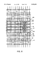
- FIG. 6 is a schematic representation of memory arrays in accordance with the embodiment of this invention.
- FIG. 7 contains a table which shows voltage conditions for various operational modes for the memory device of FIG. 6 in accordance with the embodiment of this invention
- FIG. 8 is a topological view of the memory device of FIG. 6 in accordance with the embodiment of the present invention.
- FIG. 9 is a topological view of the memory device of FIG. 6 during the process steps used in the formation of field oxide layers for isolation and in the ion implant into the regions for connecting control gates;
- FIG. 10 is a topological view of the memory device of FIG. 6 during the process steps used in the formation of control gates and floating gates;
- FIG. 11 is a topological view of the memory device of FIG. 6 during the process steps used in the ion implant into the portions of memory diffusion strips where a source region and a drain region of each memory cell are to be formed, and the portion of the memory diffusion strip connected to the region where a block select transistor is to be formed;
- FIG. 12 is a topological view of the memory device of FIG. 6 during the process steps used in the formation of select gates and gates of block select transistors;
- FIG. 13 is a topological view of the memory device of FIG. 6 during the process step used in the formation of source and drain regions of block select transistors;
- FIG. 14 is a topological view of the memory device of FIG. 6 during the process step used in the formation of contact holes;
- FIG. 15 is a topological view of the memory device of FIG. 6 during the process step used in the metallization
- FIG. 16 is a topological view of the memory device of FIG. 6 during the process steps used in the formation of through-holes in the drain regions of the block select transistors;
- FIG. 17 is a topological view of the memory device of FIG. 6 during the process step used in the formation of metal bit lines.
- a plurality of memory cells of the present invention are arranged in a matrix and are adjacent to one of a plurality of memory diffusion strips to be symmetric in the direction of the memory diffusion strip or the memory bit direction.
- a plurality of memory cells are connected to consist of memory blocks, and each memory block is defined independently of the region of the memory cells which share one single metal bit line.
- the memory diffusion layers are formed with source and drain regions of the memory cells, being divided from other memory blocks, such that each memory diffusion layer is connected to one of metal bit lines through one of block transistors that is formed in the region between two neighboring memory blocks in the bit line direction.
- control gates are formed to connect a plurality of the memory cells within the memory block such that each of the memory blocks is divided from other memory blocks, and such that a pair of the control gates which share the same drain region are connected to each other to be equipotential and to form a control gate pair.
- a plurality of control gate pairs are then connected within the memory block and this procedure is repeated for all of the control gate pairs.
- one group (the first group) of the connected pairs is connected not to another group adjacent to the first group but to the group next adjacent thereto, to thereby form two sets of control gate pairs. These two sets are each thereafter connected to polysilicon strips.
- a plurality of metal strips are formed to accomplish the connection between the memory diffusion strips.
- One of the metal strips is formed to connect a plurality of the control gate pairs.
- this metal strip traverses the portion of the memory diffusion strip which connects to the regions for block select transistors to be formed, a process step of implanting ions into these regions is carried out prior to the step of the gate oxide layer formation, the advantages of which will be described hereinbelow.
- Source and drain regions of the block select transistors may preferably be fabricated to have the same impurity concentration as that of transistors of the peripheral circuitry.
- two groups of gate electrodes of block select transistors are each formed in line, one being connected to source regions and the other connected to drain regions of the memory cells.
- the two groups are each preferably formed spaced-apart, parallel to each other and to the word line direction.
- the distance between block select transistors may be increased with the present construction to accomplish higher current values for the transistors and thereby higher readout speed for the memory device.
- a plurality of the metal bit lines in strips are provided spaced apart, being essentially parallel to, and with a distance approximately equal to that of the memory diffusion layers, having overlying dielectric layers, and thereafter connected to the block select transistors through contact holes.
- a plurality of metal word lines in strips are provided spaced apart, being essentially parallel to the select gates, and having a pitch approximately equal to that of the select gates, having overlying dielectric layers.
- the metal word lines are then connected to the select gates through contact holes that are provided on extensions of the select gates.
- the metal word lines are provided preferably under the metal bit lines.
- the capacitance between the metal bit lines and word lines can be reduced to thereby accomplish higher readout speeds for the memory device.
- overlying metal layers both in the bit line and word line directions may be fabricated so as to have the same pitch as that of memory cells. This makes it possible to eliminate the shading of the memory cells which are caused by the aforementioned difference between the pitches and to carry out an ultra violet light erasure throughout the memory cells in the device.
- a plurality of the control gates are formed also being divided by the memory block.
- the control gates within each of memory blocks are preferably connected to polysilicon strips 33a and 33b (FIG. 10).
- the polysilicon strips are thereafter connected to one of the metal lines which is formed parallel to the word line over the polysilicon strip having an underlying dielectric layer.
- a plurality of gate electrodes of the block select transistors are formed of polysilicon strips so as to be connected each other within a memory block.
- the polysilicon strip is preferably connected to one of the metal lines which is formed parallel to the word line over the polysilicon strip having an underlying dielectric layer.
- FIG. 6 illustrates a typical memory array in a memory cell matrix in accordance with one embodiment of the present invention.
- the memory cells 1 of the split gate structure are arranged in a matrix.
- the memory matrix is formed by interconnecting memory cells in a memory block in parallel with each other to memory diffusion strips 7 and 8, and each of source and drain regions are shared within the memory block through the memory diffusion strips.
- the memory diffusion strips 7 and 8 are each formed in a memory block independent of other memory blocks and are respectively connected to metal bit lines 11 and 12 through block select transistors 9 and 10.
- the memory cells are thus arranged in symmetric form in the direction of memory diffusion strips 7 and 8.
- Control gates 2 and 3 that are formed adjacent to the drain diffusion strip 8 are connected to form a control gate pair 4.
- the control gate pair 4 is then connected to every other pair of control gates (e.g., to control gate pairs 6 and 14), and not to the control gate pair 5 adjacent to the control gate pair 4.
- control gate pair 5 adjacent to the pair 4 is connected to every other control gate pair 13 and 15.
- control gate connections are made within each memory block and that no connections are made between other memory blocks.
- FIG. 7 contains a table which illustrates voltage conditions for various operational modes for the memory device according to the embodiment of the present invention.
- the potential value is shown under the row heading "Read L1 and L2", which is to be applied to each corresponding line in the FIG. 7 for carrying out the readout operation of data stored in the cells L1 and L2. Also in the table, the potential is in volts, "F” is for floating, “Erase” is for erasing all of the memory cells, and “PGM” is for programming of the write operation for each memory cell.
- FIG. 8 illustrates a top view of a circuit pattern of the memory device of FIG. 6 fabricated on a semiconductor substrate in accordance with one embodiment of the present invention.
- a plurality of floating gates 32 are formed between the source and drain regions, having a length smaller than that of from source 38 to drain 39 and at a distance closer to drain region 39 than to the source region 38.
- a plurality of control gates 33 of polysilicon are also formed over the floating gates parallel to the drain memory diffusion strip 39.
- the source diffusion and drain diffusion strips 38 and 39 are respectively shared by memory cells which are formed adjacent to the same diffusion strips and parallel to the diffusion strip direction.
- control gates 33 which are formed adjacent to the same drain are connected together through the polysilicon layers 33a and 33b to form control gate pairs, and the control gate pairs are connected to alternate control pairs, to thereby form two sets of the connected control gate pairs.
- These connected control gate pairs are formed within each of the memory blocks independent of the other memory blocks.
- a plurality of select gates 34 are also formed of polysilicon perpendicular to the control gate 33.
- the memory diffusion strips such as the source diffusion 38 and the drain diffusion strips 39 are formed within one of the memory blocks independent of other memory blocks.
- the source diffusion 38 and the drain diffusion strip 39 are then connected to block select transistors 40 and 37, respectively, and further to metal bit lines (not shown in FIG. 8) through contact holes 41 and 36.
- two groups of connected gate electrodes 35 of block select transistors 40 and 37 are each formed in line, one being connected to source regions 38 and the other connected to drain regions 39 of the memory cells.
- the two groups are formed not on the same line but spaced-apart to each other.
- the distance between block select transistors is increased with this construction to accomplish higher current values for the transistors and thereby higher readout speeds for the memory device.
- FIGS. 9 through 17 a fabrication process of the present invention will be detailed hereinbelow.
- the starting material is assumed to be P-type silicon substrate on which a field oxide layer is grown. As illustrated in FIG. 9, portions of this layer are removed for forming active regions 50, in which memory cells, block select transistors, peripheral transistors and diffusion layers are to be formed. The remainder of the field oxide is used to isolate the active regions from each other.
- an implanting step using arsenic (As) ions is carried out into the regions 53 in the active regions 50, which traverses polysilicon strips 33a and 33b to be connected to a plurality of control gates (FIG. 8).
- a gate oxide layer is then grown over the entire surface of the structure, followed by the formation of a polysilicon layer thereon, from which floating gates 32 are to be formed as shown in FIG. 10.
- the polysilicon layer is defined by etching into regions to be isolated from each other by removing portions thereof perpendicular to the bit line direction, to thereby form the floating gates 32.
- Another polysilicon layer is formed thereon, from which control gates 33 are to be formed.
- the thus formed layer comprising the following contiguous layer portions grown from the bottom in the order recited, the polysilicon layer portion for floating gates, an interpoly dielectrics portion and the polysilicon portion for the control gates, is hereinafter referred to as a floating gate polysilicon/interpoly dielectric/control gate polysilicon layer.
- the floating gate polysilicon/interpoly dielectric/control gate polysilicon layer is then subjected to an etching process step to define the layer into strips parallel to the bit line direction to thereby form floating gates 32 and control gates 33 such that these gates are capable of being operated within each memory block independent of other memory blocks.
- control gate polysilicon layer is subjected to an etching process step to form control gates in long strips running parallel to the memory bit direction such that a pair of the control gates sharing the same drain region are connected together to be equipotential and to form a control gate pair, and a plurality of control gate pairs are then connected within the memory block. This procedure is repeated for all control gate pairs.
- one group of the connected pairs (or the first group) is connected not to another group adjacent to the first group but to the next group next neighbored!, to thereby form two sets of the control gate pairs to be connected thereafter to polysilicon strips 33a and 33b.
- an implant process step is subsequently carried out with As ions into the regions such as (1) the portion of the memory diffusion strips where a source or drain region 38 and 39 of the memory cell are to be formed, and (2) the portion 57 of the memory diffusion strip connected to the region 60 where a block select transistor is to be formed.
- the portions 57 of the strips which are overlaid by the polysilicon strips 33a and 33b, are not implanted with As ions, because these control gate strips are acting as a mask against the ion implant.
- the polysilicon layer is then subjected to a patterning process to thereby form a select gate 34 and gates of the block select transistors.
- control gate strips 35 have already been implanted with As ions prior to the formation of the second gate oxide layer, as described earlier, and that an oxide layer is formed with the thickness larger than that of the gate oxide layer, which resulted from the impurity enhanced oxidation. The insulation between the memory diffusion strips and the block select transistor gates is therefore maintained.
- a dielectric layer is disposed over the entire surface of the structure to be an interlayer dielectric layer between the polysilicon and overlying metal layers. This process step is followed by the definition of a plurality of contact holes in the regions, such as drains 36 and 41 of the block select transistor, select gates 66, control gates 67 and gates of the block select transistor 68, using the conventional photolithography technology.
- the uppermost layer in the memory cell regions is generally formed more elevated from the substrate than the other regions of the memory device because of multiple layers accumulated in the cell regions.
- the block select transistors are formed between memory blocks in the present embodiment, the contact holes 36 and 41 are formed having a greater distance from the memory cells than that formed without block select transistors. This results in a decrease in the elevation of the regions for the contact holes, as described just above, and the thickness of the interlayer dielectric layer in these regions may be decreased compared to that of the peripheral circuitry.
- the diameter of contact holes increases with the increase in the thickness of interlayer dielectrics during the photolithography process.
- the thickness of the interlayer dielectrics in the contact hole forming region can be decreased in the present embodiment to an extent comparable to that of the peripheral circuitry, the difficulty in contact hole diameter and the focal depth can thus be obviated, to thereby achieve contact hole diameters in the memory cell regions approximately equal to that of surrounding circuit components.
- a metal layer of aluminum alloy is deposited over the entire surface of the structure, having the interlayer dielectric layer thereunder, and the desired metallization pattern is defined through conventional masking and metal etching techniques, as illustrated in FIG. 15.
- metal strips 69 are formed in parallel with, and over the select gates having the same pitch as that of the select gates. These strips are then connected to the select gates through contact holes 66. Also during the process steps, other metal strips are formed parallel to the word line direction and connected to the control gates through contact holes 68.
- the pattern of the metal strips can be defined with the same minimum dimension for the fabrication process as that for upper metal layers.
- the metal strips 69 can therefore be defined with the same minimum fabrication dimension as that for the memory cell, though the metal strips are perpendicular to the bit line direction or in parallel to the word line direction, as above-mentioned, which have had a minimum dimension larger than that for the bit line direction.
- a dielectric layer is disposed over the entire surface of the structure to be an inter-metal dielectric layer between metal layers, and through-holes 72 are then formed in the drain regions of the block select transistors 36 and 41.
- the thickness of the inter-metal dielectric layer in the region for forming through-holes 72 can be fabricated to be comparable to that of the peripheral circuitry, the height of these regions from the substrate can also be made comparable to that of the contact hole forming regions. Therefore, the through-hole diameter comparable to that in the surrounding device regions can be achieved.
- a metal layer of aluminum alloy is deposited over the entire surface of the structure, having an underlying inter-metal dielectric layer, and the desired metallization pattern is then defined, as illustrated in FIG. 17.
- Metal strips 73 are formed in the bit line direction, having the same pitch as that of the source and drain regions, and are connected to the drains of block transistors through holes 72 and contact holes 36 and 41.
- each of the metal bit lines 73 is required in general to preferably include an additional area in the through-hole forming regions to secure overlap due to the allowance consideration for the mask-alignment step during the photolithography process.
Abstract
Description
Claims (12)
Applications Claiming Priority (2)
| Application Number | Priority Date | Filing Date | Title |
|---|---|---|---|
| JP9-141069 | 1997-05-14 | ||
| JP14106997 | 1997-05-14 |
Publications (1)
| Publication Number | Publication Date |
|---|---|
| US5952691A true US5952691A (en) | 1999-09-14 |
Family
ID=15283523
Family Applications (1)
| Application Number | Title | Priority Date | Filing Date |
|---|---|---|---|
| US09/076,997 Expired - Fee Related US5952691A (en) | 1997-05-14 | 1998-05-13 | Non-volatile electrically alterable semiconductor memory device |
Country Status (1)
| Country | Link |
|---|---|
| US (1) | US5952691A (en) |
Cited By (6)
| Publication number | Priority date | Publication date | Assignee | Title |
|---|---|---|---|---|
| US6478231B1 (en) * | 2001-06-29 | 2002-11-12 | Hewlett Packard Company | Methods for reducing the number of interconnects to the PIRM memory module |
| US6853557B1 (en) * | 2000-09-20 | 2005-02-08 | Rambus, Inc. | Multi-channel memory architecture |
| US7177998B2 (en) | 2001-04-24 | 2007-02-13 | Rambus Inc. | Method, system and memory controller utilizing adjustable read data delay settings |
| US7301831B2 (en) | 2004-09-15 | 2007-11-27 | Rambus Inc. | Memory systems with variable delays for write data signals |
| US8320191B2 (en) | 2007-08-30 | 2012-11-27 | Infineon Technologies Ag | Memory cell arrangement, method for controlling a memory cell, memory array and electronic device |
| US8320202B2 (en) | 2001-04-24 | 2012-11-27 | Rambus Inc. | Clocked memory system with termination component |
Citations (5)
| Publication number | Priority date | Publication date | Assignee | Title |
|---|---|---|---|---|
| US5280446A (en) * | 1990-09-20 | 1994-01-18 | Bright Microelectronics, Inc. | Flash eprom memory circuit having source side programming |
| US5557154A (en) * | 1991-10-11 | 1996-09-17 | Exlar Corporation | Linear actuator with feedback position sensor device |
| US5579259A (en) * | 1995-05-31 | 1996-11-26 | Sandisk Corporation | Low voltage erase of a flash EEPROM system having a common erase electrode for two individually erasable sectors |
| US5614747A (en) * | 1994-07-28 | 1997-03-25 | Hyundai Electronics Industries Co., Ltd. | Method for manufacturing a flash EEPROM cell |
| US5633518A (en) * | 1995-07-28 | 1997-05-27 | Zycad Corporation | Nonvolatile reprogrammable interconnect cell with FN tunneling and programming method thereof |
-
1998
- 1998-05-13 US US09/076,997 patent/US5952691A/en not_active Expired - Fee Related
Patent Citations (5)
| Publication number | Priority date | Publication date | Assignee | Title |
|---|---|---|---|---|
| US5280446A (en) * | 1990-09-20 | 1994-01-18 | Bright Microelectronics, Inc. | Flash eprom memory circuit having source side programming |
| US5557154A (en) * | 1991-10-11 | 1996-09-17 | Exlar Corporation | Linear actuator with feedback position sensor device |
| US5614747A (en) * | 1994-07-28 | 1997-03-25 | Hyundai Electronics Industries Co., Ltd. | Method for manufacturing a flash EEPROM cell |
| US5579259A (en) * | 1995-05-31 | 1996-11-26 | Sandisk Corporation | Low voltage erase of a flash EEPROM system having a common erase electrode for two individually erasable sectors |
| US5633518A (en) * | 1995-07-28 | 1997-05-27 | Zycad Corporation | Nonvolatile reprogrammable interconnect cell with FN tunneling and programming method thereof |
Cited By (41)
| Publication number | Priority date | Publication date | Assignee | Title |
|---|---|---|---|---|
| US6853557B1 (en) * | 2000-09-20 | 2005-02-08 | Rambus, Inc. | Multi-channel memory architecture |
| US9311976B2 (en) | 2001-04-24 | 2016-04-12 | Rambus Inc. | Memory module |
| US8214616B2 (en) | 2001-04-24 | 2012-07-03 | Rambus Inc. | Memory controller device having timing offset capability |
| US7200055B2 (en) | 2001-04-24 | 2007-04-03 | Rambus Inc. | Memory module with termination component |
| US7210016B2 (en) | 2001-04-24 | 2007-04-24 | Rambus Inc. | Method, system and memory controller utilizing adjustable write data delay settings |
| US7209397B2 (en) | 2001-04-24 | 2007-04-24 | Rambus Inc. | Memory device with clock multiplier circuit |
| US7225292B2 (en) | 2001-04-24 | 2007-05-29 | Rambus Inc. | Memory module with termination component |
| US8395951B2 (en) | 2001-04-24 | 2013-03-12 | Rambus Inc. | Memory controller |
| US10706910B2 (en) | 2001-04-24 | 2020-07-07 | Rambus Inc. | Memory controller |
| US7484064B2 (en) | 2001-04-24 | 2009-01-27 | Rambus Inc. | Method and apparatus for signaling between devices of a memory system |
| US8462566B2 (en) | 2001-04-24 | 2013-06-11 | Rambus Inc. | Memory module with termination component |
| US7177998B2 (en) | 2001-04-24 | 2007-02-13 | Rambus Inc. | Method, system and memory controller utilizing adjustable read data delay settings |
| US8760944B2 (en) | 2001-04-24 | 2014-06-24 | Rambus Inc. | Memory component that samples command/address signals in response to both edges of a clock signal |
| US9741424B2 (en) | 2001-04-24 | 2017-08-22 | Rambus Inc. | Memory controller |
| US9472262B2 (en) | 2001-04-24 | 2016-10-18 | Rambus Inc. | Memory controller |
| US8320202B2 (en) | 2001-04-24 | 2012-11-27 | Rambus Inc. | Clocked memory system with termination component |
| US8359445B2 (en) | 2001-04-24 | 2013-01-22 | Rambus Inc. | Method and apparatus for signaling between devices of a memory system |
| US8717837B2 (en) | 2001-04-24 | 2014-05-06 | Rambus Inc. | Memory module |
| US9053778B2 (en) | 2001-04-24 | 2015-06-09 | Rambus Inc. | Memory controller that enforces strobe-to-strobe timing offset |
| US7225311B2 (en) | 2001-04-24 | 2007-05-29 | Rambus Inc. | Method and apparatus for coordinating memory operations among diversely-located memory components |
| US10236051B2 (en) | 2001-04-24 | 2019-03-19 | Rambus Inc. | Memory controller |
| US8391039B2 (en) | 2001-04-24 | 2013-03-05 | Rambus Inc. | Memory module with termination component |
| US8537601B2 (en) | 2001-04-24 | 2013-09-17 | Rambus Inc. | Memory controller with selective data transmission delay |
| US8625371B2 (en) | 2001-04-24 | 2014-01-07 | Rambus Inc. | Memory component with terminated and unterminated signaling inputs |
| US6478231B1 (en) * | 2001-06-29 | 2002-11-12 | Hewlett Packard Company | Methods for reducing the number of interconnects to the PIRM memory module |
| US8045407B2 (en) | 2004-09-15 | 2011-10-25 | Rambus Inc. | Memory-write timing calibration including generation of multiple delayed timing signals |
| US7724590B2 (en) | 2004-09-15 | 2010-05-25 | Rambus Inc. | Memory controller with multiple delayed timing signals |
| US11664067B2 (en) | 2004-09-15 | 2023-05-30 | Rambus Inc. | Memory system component that enables clock-to-strobe skew compensation |
| US8493802B1 (en) | 2004-09-15 | 2013-07-23 | Rambus Inc. | Memory controller having a write-timing calibration mode |
| US9229470B2 (en) | 2004-09-15 | 2016-01-05 | Rambus Inc. | Memory controller with clock-to-strobe skew compensation |
| US8363493B2 (en) | 2004-09-15 | 2013-01-29 | Rambus Inc. | Memory controller having a write-timing calibration mode |
| US9437279B2 (en) | 2004-09-15 | 2016-09-06 | Rambus Inc. | Memory controller with clock-to-strobe skew compensation |
| US11100976B2 (en) | 2004-09-15 | 2021-08-24 | Rambus Inc. | Memory controller with clock-to-strobe skew compensation |
| US8218382B2 (en) | 2004-09-15 | 2012-07-10 | Rambus Inc. | Memory component having a write-timing calibration mode |
| US9830971B2 (en) | 2004-09-15 | 2017-11-28 | Rambus Inc. | Memory controller with clock-to-strobe skew compensation |
| US8743636B2 (en) | 2004-09-15 | 2014-06-03 | Rambus Inc. | Memory module having a write-timing calibration mode |
| US10325645B2 (en) | 2004-09-15 | 2019-06-18 | Rambus Inc. | Memory controller with clock-to-strobe skew compensation |
| US7301831B2 (en) | 2004-09-15 | 2007-11-27 | Rambus Inc. | Memory systems with variable delays for write data signals |
| US10755764B2 (en) | 2004-09-15 | 2020-08-25 | Rambus Inc. | Memory component that enables calibrated command- and data-timing signal arrival |
| US8320191B2 (en) | 2007-08-30 | 2012-11-27 | Infineon Technologies Ag | Memory cell arrangement, method for controlling a memory cell, memory array and electronic device |
| US9030877B2 (en) | 2007-08-30 | 2015-05-12 | Infineon Technologies Ag | Memory cell arrangement, method for controlling a memory cell, memory array and electronic device |
Similar Documents
| Publication | Publication Date | Title |
|---|---|---|
| US5691938A (en) | Non-volatile memory cell and array architecture | |
| KR100217532B1 (en) | Packing density for flash memories | |
| US4267632A (en) | Process for fabricating a high density electrically programmable memory array | |
| US5793079A (en) | Single transistor non-volatile electrically alterable semiconductor memory device | |
| US7091087B2 (en) | Optimized flash memory cell | |
| US5654917A (en) | Process for making and programming a flash memory array | |
| US6285584B1 (en) | Method to implement flash memory | |
| KR930007527B1 (en) | Nonvolatile semiconductor memory device having a storage cell array and circumference circuit and method for fabricating thereof | |
| US6064592A (en) | Non-volatile semiconductor memory featuring effective cell area reduction using contactless technology | |
| US6239500B1 (en) | Semiconductor device with common bit contact area | |
| JP3233998B2 (en) | Manufacturing method of nonvolatile semiconductor memory device | |
| US5162247A (en) | Process for trench-isolated self-aligned split-gate EEPROM transistor and memory array | |
| US5414286A (en) | Nonvolatile memory, method of fabricating the same, and method of reading information from the same | |
| KR0155859B1 (en) | Flash memory device & its fabricating method | |
| US7180788B2 (en) | Nonvolatile semiconductor memory device | |
| US6001688A (en) | Method of eliminating poly stringer in a memory device | |
| US5952691A (en) | Non-volatile electrically alterable semiconductor memory device | |
| US20020135013A1 (en) | Segmented bit line EEPROM page architecture | |
| JP2003051557A (en) | Nonvolatile semiconductor storage device | |
| KR19980055726A (en) | Flash memory device and program, erase and read method using same | |
| US5216270A (en) | Non-volatile memory cell with tunnel window structure and method | |
| JP3226589B2 (en) | Manufacturing method of nonvolatile semiconductor memory device | |
| KR100650837B1 (en) | Nand flash memory device and method for fabricating nand flash memory device | |
| US5151760A (en) | Integrated circuit with improved capacitive coupling | |
| KR100289814B1 (en) | Non-volatile memory device and method for manufacturing the same |
Legal Events
| Date | Code | Title | Description |
|---|---|---|---|
| AS | Assignment |
Owner name: RICOH COMPANY, LTD., JAPAN Free format text: ASSIGNMENT OF ASSIGNORS INTEREST;ASSIGNOR:YAMAGUCHI, KIYOSHI;REEL/FRAME:009343/0968 Effective date: 19980702 |
|
| FEPP | Fee payment procedure |
Free format text: PAYOR NUMBER ASSIGNED (ORIGINAL EVENT CODE: ASPN); ENTITY STATUS OF PATENT OWNER: LARGE ENTITY |
|
| FPAY | Fee payment |
Year of fee payment: 4 |
|
| REMI | Maintenance fee reminder mailed | ||
| FPAY | Fee payment |
Year of fee payment: 8 |
|
| FEPP | Fee payment procedure |
Free format text: PAYOR NUMBER ASSIGNED (ORIGINAL EVENT CODE: ASPN); ENTITY STATUS OF PATENT OWNER: LARGE ENTITY Free format text: PAYER NUMBER DE-ASSIGNED (ORIGINAL EVENT CODE: RMPN); ENTITY STATUS OF PATENT OWNER: LARGE ENTITY |
|
| REMI | Maintenance fee reminder mailed | ||
| LAPS | Lapse for failure to pay maintenance fees | ||
| STCH | Information on status: patent discontinuation |
Free format text: PATENT EXPIRED DUE TO NONPAYMENT OF MAINTENANCE FEES UNDER 37 CFR 1.362 |
|
| FP | Lapsed due to failure to pay maintenance fee |
Effective date: 20110914 |