US5953589A - Ball grid array semiconductor package with solder balls fused on printed circuit board and method for fabricating the same - Google Patents
Ball grid array semiconductor package with solder balls fused on printed circuit board and method for fabricating the same Download PDFInfo
- Publication number
- US5953589A US5953589A US08/915,077 US91507797A US5953589A US 5953589 A US5953589 A US 5953589A US 91507797 A US91507797 A US 91507797A US 5953589 A US5953589 A US 5953589A
- Authority
- US
- United States
- Prior art keywords
- circuit board
- flexible circuit
- support plate
- carrier frame
- outer support
- Prior art date
- Legal status (The legal status is an assumption and is not a legal conclusion. Google has not performed a legal analysis and makes no representation as to the accuracy of the status listed.)
- Expired - Lifetime
Links
Images


Classifications
-
- H—ELECTRICITY
- H01—ELECTRIC ELEMENTS
- H01L—SEMICONDUCTOR DEVICES NOT COVERED BY CLASS H10
- H01L24/00—Arrangements for connecting or disconnecting semiconductor or solid-state bodies; Methods or apparatus related thereto
- H01L24/01—Means for bonding being attached to, or being formed on, the surface to be connected, e.g. chip-to-package, die-attach, "first-level" interconnects; Manufacturing methods related thereto
- H01L24/26—Layer connectors, e.g. plate connectors, solder or adhesive layers; Manufacturing methods related thereto
- H01L24/31—Structure, shape, material or disposition of the layer connectors after the connecting process
- H01L24/32—Structure, shape, material or disposition of the layer connectors after the connecting process of an individual layer connector
-
- H—ELECTRICITY
- H01—ELECTRIC ELEMENTS
- H01L—SEMICONDUCTOR DEVICES NOT COVERED BY CLASS H10
- H01L21/00—Processes or apparatus adapted for the manufacture or treatment of semiconductor or solid state devices or of parts thereof
- H01L21/02—Manufacture or treatment of semiconductor devices or of parts thereof
- H01L21/04—Manufacture or treatment of semiconductor devices or of parts thereof the devices having at least one potential-jump barrier or surface barrier, e.g. PN junction, depletion layer or carrier concentration layer
- H01L21/50—Assembly of semiconductor devices using processes or apparatus not provided for in a single one of the subgroups H01L21/06 - H01L21/326, e.g. sealing of a cap to a base of a container
- H01L21/56—Encapsulations, e.g. encapsulation layers, coatings
- H01L21/565—Moulds
-
- H—ELECTRICITY
- H01—ELECTRIC ELEMENTS
- H01L—SEMICONDUCTOR DEVICES NOT COVERED BY CLASS H10
- H01L23/00—Details of semiconductor or other solid state devices
- H01L23/34—Arrangements for cooling, heating, ventilating or temperature compensation ; Temperature sensing arrangements
- H01L23/42—Fillings or auxiliary members in containers or encapsulations selected or arranged to facilitate heating or cooling
- H01L23/433—Auxiliary members in containers characterised by their shape, e.g. pistons
- H01L23/4334—Auxiliary members in encapsulations
-
- H—ELECTRICITY
- H01—ELECTRIC ELEMENTS
- H01L—SEMICONDUCTOR DEVICES NOT COVERED BY CLASS H10
- H01L23/00—Details of semiconductor or other solid state devices
- H01L23/48—Arrangements for conducting electric current to or from the solid state body in operation, e.g. leads, terminal arrangements ; Selection of materials therefor
- H01L23/488—Arrangements for conducting electric current to or from the solid state body in operation, e.g. leads, terminal arrangements ; Selection of materials therefor consisting of soldered or bonded constructions
- H01L23/498—Leads, i.e. metallisations or lead-frames on insulating substrates, e.g. chip carriers
- H01L23/49811—Additional leads joined to the metallisation on the insulating substrate, e.g. pins, bumps, wires, flat leads
- H01L23/49816—Spherical bumps on the substrate for external connection, e.g. ball grid arrays [BGA]
-
- H—ELECTRICITY
- H01—ELECTRIC ELEMENTS
- H01L—SEMICONDUCTOR DEVICES NOT COVERED BY CLASS H10
- H01L23/00—Details of semiconductor or other solid state devices
- H01L23/48—Arrangements for conducting electric current to or from the solid state body in operation, e.g. leads, terminal arrangements ; Selection of materials therefor
- H01L23/488—Arrangements for conducting electric current to or from the solid state body in operation, e.g. leads, terminal arrangements ; Selection of materials therefor consisting of soldered or bonded constructions
- H01L23/498—Leads, i.e. metallisations or lead-frames on insulating substrates, e.g. chip carriers
- H01L23/4985—Flexible insulating substrates
-
- H—ELECTRICITY
- H01—ELECTRIC ELEMENTS
- H01L—SEMICONDUCTOR DEVICES NOT COVERED BY CLASS H10
- H01L24/00—Arrangements for connecting or disconnecting semiconductor or solid-state bodies; Methods or apparatus related thereto
- H01L24/01—Means for bonding being attached to, or being formed on, the surface to be connected, e.g. chip-to-package, die-attach, "first-level" interconnects; Manufacturing methods related thereto
- H01L24/42—Wire connectors; Manufacturing methods related thereto
- H01L24/47—Structure, shape, material or disposition of the wire connectors after the connecting process
- H01L24/48—Structure, shape, material or disposition of the wire connectors after the connecting process of an individual wire connector
-
- H—ELECTRICITY
- H01—ELECTRIC ELEMENTS
- H01L—SEMICONDUCTOR DEVICES NOT COVERED BY CLASS H10
- H01L24/00—Arrangements for connecting or disconnecting semiconductor or solid-state bodies; Methods or apparatus related thereto
- H01L24/80—Methods for connecting semiconductor or other solid state bodies using means for bonding being attached to, or being formed on, the surface to be connected
- H01L24/83—Methods for connecting semiconductor or other solid state bodies using means for bonding being attached to, or being formed on, the surface to be connected using a layer connector
-
- H—ELECTRICITY
- H01—ELECTRIC ELEMENTS
- H01L—SEMICONDUCTOR DEVICES NOT COVERED BY CLASS H10
- H01L2224/00—Indexing scheme for arrangements for connecting or disconnecting semiconductor or solid-state bodies and methods related thereto as covered by H01L24/00
- H01L2224/01—Means for bonding being attached to, or being formed on, the surface to be connected, e.g. chip-to-package, die-attach, "first-level" interconnects; Manufacturing methods related thereto
- H01L2224/26—Layer connectors, e.g. plate connectors, solder or adhesive layers; Manufacturing methods related thereto
- H01L2224/2612—Auxiliary members for layer connectors, e.g. spacers
-
- H—ELECTRICITY
- H01—ELECTRIC ELEMENTS
- H01L—SEMICONDUCTOR DEVICES NOT COVERED BY CLASS H10
- H01L2224/00—Indexing scheme for arrangements for connecting or disconnecting semiconductor or solid-state bodies and methods related thereto as covered by H01L24/00
- H01L2224/01—Means for bonding being attached to, or being formed on, the surface to be connected, e.g. chip-to-package, die-attach, "first-level" interconnects; Manufacturing methods related thereto
- H01L2224/26—Layer connectors, e.g. plate connectors, solder or adhesive layers; Manufacturing methods related thereto
- H01L2224/28—Structure, shape, material or disposition of the layer connectors prior to the connecting process
- H01L2224/29—Structure, shape, material or disposition of the layer connectors prior to the connecting process of an individual layer connector
- H01L2224/29001—Core members of the layer connector
- H01L2224/29099—Material
- H01L2224/291—Material with a principal constituent of the material being a metal or a metalloid, e.g. boron [B], silicon [Si], germanium [Ge], arsenic [As], antimony [Sb], tellurium [Te] and polonium [Po], and alloys thereof
- H01L2224/29101—Material with a principal constituent of the material being a metal or a metalloid, e.g. boron [B], silicon [Si], germanium [Ge], arsenic [As], antimony [Sb], tellurium [Te] and polonium [Po], and alloys thereof the principal constituent melting at a temperature of less than 400°C
- H01L2224/29111—Tin [Sn] as principal constituent
-
- H—ELECTRICITY
- H01—ELECTRIC ELEMENTS
- H01L—SEMICONDUCTOR DEVICES NOT COVERED BY CLASS H10
- H01L2224/00—Indexing scheme for arrangements for connecting or disconnecting semiconductor or solid-state bodies and methods related thereto as covered by H01L24/00
- H01L2224/01—Means for bonding being attached to, or being formed on, the surface to be connected, e.g. chip-to-package, die-attach, "first-level" interconnects; Manufacturing methods related thereto
- H01L2224/26—Layer connectors, e.g. plate connectors, solder or adhesive layers; Manufacturing methods related thereto
- H01L2224/28—Structure, shape, material or disposition of the layer connectors prior to the connecting process
- H01L2224/29—Structure, shape, material or disposition of the layer connectors prior to the connecting process of an individual layer connector
- H01L2224/29001—Core members of the layer connector
- H01L2224/29099—Material
- H01L2224/2919—Material with a principal constituent of the material being a polymer, e.g. polyester, phenolic based polymer, epoxy
-
- H—ELECTRICITY
- H01—ELECTRIC ELEMENTS
- H01L—SEMICONDUCTOR DEVICES NOT COVERED BY CLASS H10
- H01L2224/00—Indexing scheme for arrangements for connecting or disconnecting semiconductor or solid-state bodies and methods related thereto as covered by H01L24/00
- H01L2224/01—Means for bonding being attached to, or being formed on, the surface to be connected, e.g. chip-to-package, die-attach, "first-level" interconnects; Manufacturing methods related thereto
- H01L2224/26—Layer connectors, e.g. plate connectors, solder or adhesive layers; Manufacturing methods related thereto
- H01L2224/31—Structure, shape, material or disposition of the layer connectors after the connecting process
- H01L2224/32—Structure, shape, material or disposition of the layer connectors after the connecting process of an individual layer connector
- H01L2224/321—Disposition
- H01L2224/32151—Disposition the layer connector connecting between a semiconductor or solid-state body and an item not being a semiconductor or solid-state body, e.g. chip-to-substrate, chip-to-passive
- H01L2224/32221—Disposition the layer connector connecting between a semiconductor or solid-state body and an item not being a semiconductor or solid-state body, e.g. chip-to-substrate, chip-to-passive the body and the item being stacked
- H01L2224/32225—Disposition the layer connector connecting between a semiconductor or solid-state body and an item not being a semiconductor or solid-state body, e.g. chip-to-substrate, chip-to-passive the body and the item being stacked the item being non-metallic, e.g. insulating substrate with or without metallisation
-
- H—ELECTRICITY
- H01—ELECTRIC ELEMENTS
- H01L—SEMICONDUCTOR DEVICES NOT COVERED BY CLASS H10
- H01L2224/00—Indexing scheme for arrangements for connecting or disconnecting semiconductor or solid-state bodies and methods related thereto as covered by H01L24/00
- H01L2224/01—Means for bonding being attached to, or being formed on, the surface to be connected, e.g. chip-to-package, die-attach, "first-level" interconnects; Manufacturing methods related thereto
- H01L2224/42—Wire connectors; Manufacturing methods related thereto
- H01L2224/44—Structure, shape, material or disposition of the wire connectors prior to the connecting process
- H01L2224/45—Structure, shape, material or disposition of the wire connectors prior to the connecting process of an individual wire connector
- H01L2224/45001—Core members of the connector
- H01L2224/45099—Material
- H01L2224/451—Material with a principal constituent of the material being a metal or a metalloid, e.g. boron (B), silicon (Si), germanium (Ge), arsenic (As), antimony (Sb), tellurium (Te) and polonium (Po), and alloys thereof
- H01L2224/45117—Material with a principal constituent of the material being a metal or a metalloid, e.g. boron (B), silicon (Si), germanium (Ge), arsenic (As), antimony (Sb), tellurium (Te) and polonium (Po), and alloys thereof the principal constituent melting at a temperature of greater than or equal to 400°C and less than 950°C
- H01L2224/45124—Aluminium (Al) as principal constituent
-
- H—ELECTRICITY
- H01—ELECTRIC ELEMENTS
- H01L—SEMICONDUCTOR DEVICES NOT COVERED BY CLASS H10
- H01L2224/00—Indexing scheme for arrangements for connecting or disconnecting semiconductor or solid-state bodies and methods related thereto as covered by H01L24/00
- H01L2224/01—Means for bonding being attached to, or being formed on, the surface to be connected, e.g. chip-to-package, die-attach, "first-level" interconnects; Manufacturing methods related thereto
- H01L2224/42—Wire connectors; Manufacturing methods related thereto
- H01L2224/44—Structure, shape, material or disposition of the wire connectors prior to the connecting process
- H01L2224/45—Structure, shape, material or disposition of the wire connectors prior to the connecting process of an individual wire connector
- H01L2224/45001—Core members of the connector
- H01L2224/45099—Material
- H01L2224/451—Material with a principal constituent of the material being a metal or a metalloid, e.g. boron (B), silicon (Si), germanium (Ge), arsenic (As), antimony (Sb), tellurium (Te) and polonium (Po), and alloys thereof
- H01L2224/45138—Material with a principal constituent of the material being a metal or a metalloid, e.g. boron (B), silicon (Si), germanium (Ge), arsenic (As), antimony (Sb), tellurium (Te) and polonium (Po), and alloys thereof the principal constituent melting at a temperature of greater than or equal to 950°C and less than 1550°C
- H01L2224/45144—Gold (Au) as principal constituent
-
- H—ELECTRICITY
- H01—ELECTRIC ELEMENTS
- H01L—SEMICONDUCTOR DEVICES NOT COVERED BY CLASS H10
- H01L2224/00—Indexing scheme for arrangements for connecting or disconnecting semiconductor or solid-state bodies and methods related thereto as covered by H01L24/00
- H01L2224/01—Means for bonding being attached to, or being formed on, the surface to be connected, e.g. chip-to-package, die-attach, "first-level" interconnects; Manufacturing methods related thereto
- H01L2224/42—Wire connectors; Manufacturing methods related thereto
- H01L2224/47—Structure, shape, material or disposition of the wire connectors after the connecting process
- H01L2224/48—Structure, shape, material or disposition of the wire connectors after the connecting process of an individual wire connector
- H01L2224/4805—Shape
- H01L2224/4809—Loop shape
- H01L2224/48091—Arched
-
- H—ELECTRICITY
- H01—ELECTRIC ELEMENTS
- H01L—SEMICONDUCTOR DEVICES NOT COVERED BY CLASS H10
- H01L2224/00—Indexing scheme for arrangements for connecting or disconnecting semiconductor or solid-state bodies and methods related thereto as covered by H01L24/00
- H01L2224/01—Means for bonding being attached to, or being formed on, the surface to be connected, e.g. chip-to-package, die-attach, "first-level" interconnects; Manufacturing methods related thereto
- H01L2224/42—Wire connectors; Manufacturing methods related thereto
- H01L2224/47—Structure, shape, material or disposition of the wire connectors after the connecting process
- H01L2224/48—Structure, shape, material or disposition of the wire connectors after the connecting process of an individual wire connector
- H01L2224/481—Disposition
- H01L2224/48151—Connecting between a semiconductor or solid-state body and an item not being a semiconductor or solid-state body, e.g. chip-to-substrate, chip-to-passive
- H01L2224/48221—Connecting between a semiconductor or solid-state body and an item not being a semiconductor or solid-state body, e.g. chip-to-substrate, chip-to-passive the body and the item being stacked
- H01L2224/48225—Connecting between a semiconductor or solid-state body and an item not being a semiconductor or solid-state body, e.g. chip-to-substrate, chip-to-passive the body and the item being stacked the item being non-metallic, e.g. insulating substrate with or without metallisation
- H01L2224/48227—Connecting between a semiconductor or solid-state body and an item not being a semiconductor or solid-state body, e.g. chip-to-substrate, chip-to-passive the body and the item being stacked the item being non-metallic, e.g. insulating substrate with or without metallisation connecting the wire to a bond pad of the item
- H01L2224/48228—Connecting between a semiconductor or solid-state body and an item not being a semiconductor or solid-state body, e.g. chip-to-substrate, chip-to-passive the body and the item being stacked the item being non-metallic, e.g. insulating substrate with or without metallisation connecting the wire to a bond pad of the item the bond pad being disposed in a recess of the surface of the item
-
- H—ELECTRICITY
- H01—ELECTRIC ELEMENTS
- H01L—SEMICONDUCTOR DEVICES NOT COVERED BY CLASS H10
- H01L2224/00—Indexing scheme for arrangements for connecting or disconnecting semiconductor or solid-state bodies and methods related thereto as covered by H01L24/00
- H01L2224/01—Means for bonding being attached to, or being formed on, the surface to be connected, e.g. chip-to-package, die-attach, "first-level" interconnects; Manufacturing methods related thereto
- H01L2224/42—Wire connectors; Manufacturing methods related thereto
- H01L2224/47—Structure, shape, material or disposition of the wire connectors after the connecting process
- H01L2224/48—Structure, shape, material or disposition of the wire connectors after the connecting process of an individual wire connector
- H01L2224/484—Connecting portions
-
- H—ELECTRICITY
- H01—ELECTRIC ELEMENTS
- H01L—SEMICONDUCTOR DEVICES NOT COVERED BY CLASS H10
- H01L2224/00—Indexing scheme for arrangements for connecting or disconnecting semiconductor or solid-state bodies and methods related thereto as covered by H01L24/00
- H01L2224/01—Means for bonding being attached to, or being formed on, the surface to be connected, e.g. chip-to-package, die-attach, "first-level" interconnects; Manufacturing methods related thereto
- H01L2224/42—Wire connectors; Manufacturing methods related thereto
- H01L2224/47—Structure, shape, material or disposition of the wire connectors after the connecting process
- H01L2224/48—Structure, shape, material or disposition of the wire connectors after the connecting process of an individual wire connector
- H01L2224/485—Material
- H01L2224/48505—Material at the bonding interface
- H01L2224/48599—Principal constituent of the connecting portion of the wire connector being Gold (Au)
-
- H—ELECTRICITY
- H01—ELECTRIC ELEMENTS
- H01L—SEMICONDUCTOR DEVICES NOT COVERED BY CLASS H10
- H01L2224/00—Indexing scheme for arrangements for connecting or disconnecting semiconductor or solid-state bodies and methods related thereto as covered by H01L24/00
- H01L2224/01—Means for bonding being attached to, or being formed on, the surface to be connected, e.g. chip-to-package, die-attach, "first-level" interconnects; Manufacturing methods related thereto
- H01L2224/42—Wire connectors; Manufacturing methods related thereto
- H01L2224/47—Structure, shape, material or disposition of the wire connectors after the connecting process
- H01L2224/48—Structure, shape, material or disposition of the wire connectors after the connecting process of an individual wire connector
- H01L2224/485—Material
- H01L2224/48505—Material at the bonding interface
- H01L2224/48699—Principal constituent of the connecting portion of the wire connector being Aluminium (Al)
-
- H—ELECTRICITY
- H01—ELECTRIC ELEMENTS
- H01L—SEMICONDUCTOR DEVICES NOT COVERED BY CLASS H10
- H01L2224/00—Indexing scheme for arrangements for connecting or disconnecting semiconductor or solid-state bodies and methods related thereto as covered by H01L24/00
- H01L2224/73—Means for bonding being of different types provided for in two or more of groups H01L2224/10, H01L2224/18, H01L2224/26, H01L2224/34, H01L2224/42, H01L2224/50, H01L2224/63, H01L2224/71
- H01L2224/732—Location after the connecting process
- H01L2224/73251—Location after the connecting process on different surfaces
- H01L2224/73265—Layer and wire connectors
-
- H—ELECTRICITY
- H01—ELECTRIC ELEMENTS
- H01L—SEMICONDUCTOR DEVICES NOT COVERED BY CLASS H10
- H01L2224/00—Indexing scheme for arrangements for connecting or disconnecting semiconductor or solid-state bodies and methods related thereto as covered by H01L24/00
- H01L2224/80—Methods for connecting semiconductor or other solid state bodies using means for bonding being attached to, or being formed on, the surface to be connected
- H01L2224/83—Methods for connecting semiconductor or other solid state bodies using means for bonding being attached to, or being formed on, the surface to be connected using a layer connector
- H01L2224/8319—Arrangement of the layer connectors prior to mounting
- H01L2224/83192—Arrangement of the layer connectors prior to mounting wherein the layer connectors are disposed only on another item or body to be connected to the semiconductor or solid-state body
-
- H—ELECTRICITY
- H01—ELECTRIC ELEMENTS
- H01L—SEMICONDUCTOR DEVICES NOT COVERED BY CLASS H10
- H01L2224/00—Indexing scheme for arrangements for connecting or disconnecting semiconductor or solid-state bodies and methods related thereto as covered by H01L24/00
- H01L2224/91—Methods for connecting semiconductor or solid state bodies including different methods provided for in two or more of groups H01L2224/80 - H01L2224/90
- H01L2224/92—Specific sequence of method steps
- H01L2224/922—Connecting different surfaces of the semiconductor or solid-state body with connectors of different types
- H01L2224/9222—Sequential connecting processes
- H01L2224/92242—Sequential connecting processes the first connecting process involving a layer connector
- H01L2224/92247—Sequential connecting processes the first connecting process involving a layer connector the second connecting process involving a wire connector
-
- H—ELECTRICITY
- H01—ELECTRIC ELEMENTS
- H01L—SEMICONDUCTOR DEVICES NOT COVERED BY CLASS H10
- H01L24/00—Arrangements for connecting or disconnecting semiconductor or solid-state bodies; Methods or apparatus related thereto
- H01L24/01—Means for bonding being attached to, or being formed on, the surface to be connected, e.g. chip-to-package, die-attach, "first-level" interconnects; Manufacturing methods related thereto
- H01L24/42—Wire connectors; Manufacturing methods related thereto
- H01L24/44—Structure, shape, material or disposition of the wire connectors prior to the connecting process
- H01L24/45—Structure, shape, material or disposition of the wire connectors prior to the connecting process of an individual wire connector
-
- H—ELECTRICITY
- H01—ELECTRIC ELEMENTS
- H01L—SEMICONDUCTOR DEVICES NOT COVERED BY CLASS H10
- H01L24/00—Arrangements for connecting or disconnecting semiconductor or solid-state bodies; Methods or apparatus related thereto
- H01L24/73—Means for bonding being of different types provided for in two or more of groups H01L24/10, H01L24/18, H01L24/26, H01L24/34, H01L24/42, H01L24/50, H01L24/63, H01L24/71
-
- H—ELECTRICITY
- H01—ELECTRIC ELEMENTS
- H01L—SEMICONDUCTOR DEVICES NOT COVERED BY CLASS H10
- H01L2924/00—Indexing scheme for arrangements or methods for connecting or disconnecting semiconductor or solid-state bodies as covered by H01L24/00
- H01L2924/0001—Technical content checked by a classifier
- H01L2924/00014—Technical content checked by a classifier the subject-matter covered by the group, the symbol of which is combined with the symbol of this group, being disclosed without further technical details
-
- H—ELECTRICITY
- H01—ELECTRIC ELEMENTS
- H01L—SEMICONDUCTOR DEVICES NOT COVERED BY CLASS H10
- H01L2924/00—Indexing scheme for arrangements or methods for connecting or disconnecting semiconductor or solid-state bodies as covered by H01L24/00
- H01L2924/01—Chemical elements
- H01L2924/01005—Boron [B]
-
- H—ELECTRICITY
- H01—ELECTRIC ELEMENTS
- H01L—SEMICONDUCTOR DEVICES NOT COVERED BY CLASS H10
- H01L2924/00—Indexing scheme for arrangements or methods for connecting or disconnecting semiconductor or solid-state bodies as covered by H01L24/00
- H01L2924/01—Chemical elements
- H01L2924/01006—Carbon [C]
-
- H—ELECTRICITY
- H01—ELECTRIC ELEMENTS
- H01L—SEMICONDUCTOR DEVICES NOT COVERED BY CLASS H10
- H01L2924/00—Indexing scheme for arrangements or methods for connecting or disconnecting semiconductor or solid-state bodies as covered by H01L24/00
- H01L2924/01—Chemical elements
- H01L2924/01013—Aluminum [Al]
-
- H—ELECTRICITY
- H01—ELECTRIC ELEMENTS
- H01L—SEMICONDUCTOR DEVICES NOT COVERED BY CLASS H10
- H01L2924/00—Indexing scheme for arrangements or methods for connecting or disconnecting semiconductor or solid-state bodies as covered by H01L24/00
- H01L2924/01—Chemical elements
- H01L2924/01028—Nickel [Ni]
-
- H—ELECTRICITY
- H01—ELECTRIC ELEMENTS
- H01L—SEMICONDUCTOR DEVICES NOT COVERED BY CLASS H10
- H01L2924/00—Indexing scheme for arrangements or methods for connecting or disconnecting semiconductor or solid-state bodies as covered by H01L24/00
- H01L2924/01—Chemical elements
- H01L2924/01029—Copper [Cu]
-
- H—ELECTRICITY
- H01—ELECTRIC ELEMENTS
- H01L—SEMICONDUCTOR DEVICES NOT COVERED BY CLASS H10
- H01L2924/00—Indexing scheme for arrangements or methods for connecting or disconnecting semiconductor or solid-state bodies as covered by H01L24/00
- H01L2924/01—Chemical elements
- H01L2924/01047—Silver [Ag]
-
- H—ELECTRICITY
- H01—ELECTRIC ELEMENTS
- H01L—SEMICONDUCTOR DEVICES NOT COVERED BY CLASS H10
- H01L2924/00—Indexing scheme for arrangements or methods for connecting or disconnecting semiconductor or solid-state bodies as covered by H01L24/00
- H01L2924/01—Chemical elements
- H01L2924/0105—Tin [Sn]
-
- H—ELECTRICITY
- H01—ELECTRIC ELEMENTS
- H01L—SEMICONDUCTOR DEVICES NOT COVERED BY CLASS H10
- H01L2924/00—Indexing scheme for arrangements or methods for connecting or disconnecting semiconductor or solid-state bodies as covered by H01L24/00
- H01L2924/01—Chemical elements
- H01L2924/01078—Platinum [Pt]
-
- H—ELECTRICITY
- H01—ELECTRIC ELEMENTS
- H01L—SEMICONDUCTOR DEVICES NOT COVERED BY CLASS H10
- H01L2924/00—Indexing scheme for arrangements or methods for connecting or disconnecting semiconductor or solid-state bodies as covered by H01L24/00
- H01L2924/01—Chemical elements
- H01L2924/01079—Gold [Au]
-
- H—ELECTRICITY
- H01—ELECTRIC ELEMENTS
- H01L—SEMICONDUCTOR DEVICES NOT COVERED BY CLASS H10
- H01L2924/00—Indexing scheme for arrangements or methods for connecting or disconnecting semiconductor or solid-state bodies as covered by H01L24/00
- H01L2924/013—Alloys
- H01L2924/0132—Binary Alloys
-
- H—ELECTRICITY
- H01—ELECTRIC ELEMENTS
- H01L—SEMICONDUCTOR DEVICES NOT COVERED BY CLASS H10
- H01L2924/00—Indexing scheme for arrangements or methods for connecting or disconnecting semiconductor or solid-state bodies as covered by H01L24/00
- H01L2924/013—Alloys
- H01L2924/014—Solder alloys
-
- H—ELECTRICITY
- H01—ELECTRIC ELEMENTS
- H01L—SEMICONDUCTOR DEVICES NOT COVERED BY CLASS H10
- H01L2924/00—Indexing scheme for arrangements or methods for connecting or disconnecting semiconductor or solid-state bodies as covered by H01L24/00
- H01L2924/10—Details of semiconductor or other solid state devices to be connected
- H01L2924/11—Device type
- H01L2924/14—Integrated circuits
-
- H—ELECTRICITY
- H01—ELECTRIC ELEMENTS
- H01L—SEMICONDUCTOR DEVICES NOT COVERED BY CLASS H10
- H01L2924/00—Indexing scheme for arrangements or methods for connecting or disconnecting semiconductor or solid-state bodies as covered by H01L24/00
- H01L2924/15—Details of package parts other than the semiconductor or other solid state devices to be connected
- H01L2924/151—Die mounting substrate
- H01L2924/1517—Multilayer substrate
- H01L2924/15172—Fan-out arrangement of the internal vias
- H01L2924/15173—Fan-out arrangement of the internal vias in a single layer of the multilayer substrate
-
- H—ELECTRICITY
- H01—ELECTRIC ELEMENTS
- H01L—SEMICONDUCTOR DEVICES NOT COVERED BY CLASS H10
- H01L2924/00—Indexing scheme for arrangements or methods for connecting or disconnecting semiconductor or solid-state bodies as covered by H01L24/00
- H01L2924/15—Details of package parts other than the semiconductor or other solid state devices to be connected
- H01L2924/151—Die mounting substrate
- H01L2924/153—Connection portion
- H01L2924/1531—Connection portion the connection portion being formed only on the surface of the substrate opposite to the die mounting surface
- H01L2924/15311—Connection portion the connection portion being formed only on the surface of the substrate opposite to the die mounting surface being a ball array, e.g. BGA
-
- H—ELECTRICITY
- H01—ELECTRIC ELEMENTS
- H01L—SEMICONDUCTOR DEVICES NOT COVERED BY CLASS H10
- H01L2924/00—Indexing scheme for arrangements or methods for connecting or disconnecting semiconductor or solid-state bodies as covered by H01L24/00
- H01L2924/15—Details of package parts other than the semiconductor or other solid state devices to be connected
- H01L2924/151—Die mounting substrate
- H01L2924/156—Material
- H01L2924/157—Material with a principal constituent of the material being a metal or a metalloid, e.g. boron [B], silicon [Si], germanium [Ge], arsenic [As], antimony [Sb], tellurium [Te] and polonium [Po], and alloys thereof
- H01L2924/15717—Material with a principal constituent of the material being a metal or a metalloid, e.g. boron [B], silicon [Si], germanium [Ge], arsenic [As], antimony [Sb], tellurium [Te] and polonium [Po], and alloys thereof the principal constituent melting at a temperature of greater than or equal to 400 C and less than 950 C
- H01L2924/15724—Aluminium [Al] as principal constituent
-
- H—ELECTRICITY
- H01—ELECTRIC ELEMENTS
- H01L—SEMICONDUCTOR DEVICES NOT COVERED BY CLASS H10
- H01L2924/00—Indexing scheme for arrangements or methods for connecting or disconnecting semiconductor or solid-state bodies as covered by H01L24/00
- H01L2924/15—Details of package parts other than the semiconductor or other solid state devices to be connected
- H01L2924/151—Die mounting substrate
- H01L2924/156—Material
- H01L2924/157—Material with a principal constituent of the material being a metal or a metalloid, e.g. boron [B], silicon [Si], germanium [Ge], arsenic [As], antimony [Sb], tellurium [Te] and polonium [Po], and alloys thereof
- H01L2924/15738—Material with a principal constituent of the material being a metal or a metalloid, e.g. boron [B], silicon [Si], germanium [Ge], arsenic [As], antimony [Sb], tellurium [Te] and polonium [Po], and alloys thereof the principal constituent melting at a temperature of greater than or equal to 950 C and less than 1550 C
- H01L2924/15747—Copper [Cu] as principal constituent
-
- H—ELECTRICITY
- H01—ELECTRIC ELEMENTS
- H01L—SEMICONDUCTOR DEVICES NOT COVERED BY CLASS H10
- H01L2924/00—Indexing scheme for arrangements or methods for connecting or disconnecting semiconductor or solid-state bodies as covered by H01L24/00
- H01L2924/15—Details of package parts other than the semiconductor or other solid state devices to be connected
- H01L2924/151—Die mounting substrate
- H01L2924/156—Material
- H01L2924/1579—Material with a principal constituent of the material being a polymer, e.g. polyester, phenolic based polymer, epoxy
-
- H—ELECTRICITY
- H01—ELECTRIC ELEMENTS
- H01L—SEMICONDUCTOR DEVICES NOT COVERED BY CLASS H10
- H01L2924/00—Indexing scheme for arrangements or methods for connecting or disconnecting semiconductor or solid-state bodies as covered by H01L24/00
- H01L2924/15—Details of package parts other than the semiconductor or other solid state devices to be connected
- H01L2924/181—Encapsulation
- H01L2924/1815—Shape
-
- H—ELECTRICITY
- H01—ELECTRIC ELEMENTS
- H01L—SEMICONDUCTOR DEVICES NOT COVERED BY CLASS H10
- H01L2924/00—Indexing scheme for arrangements or methods for connecting or disconnecting semiconductor or solid-state bodies as covered by H01L24/00
- H01L2924/30—Technical effects
- H01L2924/301—Electrical effects
- H01L2924/30105—Capacitance
-
- H—ELECTRICITY
- H01—ELECTRIC ELEMENTS
- H01L—SEMICONDUCTOR DEVICES NOT COVERED BY CLASS H10
- H01L2924/00—Indexing scheme for arrangements or methods for connecting or disconnecting semiconductor or solid-state bodies as covered by H01L24/00
- H01L2924/30—Technical effects
- H01L2924/301—Electrical effects
- H01L2924/30107—Inductance
-
- H—ELECTRICITY
- H01—ELECTRIC ELEMENTS
- H01L—SEMICONDUCTOR DEVICES NOT COVERED BY CLASS H10
- H01L2924/00—Indexing scheme for arrangements or methods for connecting or disconnecting semiconductor or solid-state bodies as covered by H01L24/00
- H01L2924/30—Technical effects
- H01L2924/301—Electrical effects
- H01L2924/3011—Impedance
-
- H—ELECTRICITY
- H01—ELECTRIC ELEMENTS
- H01L—SEMICONDUCTOR DEVICES NOT COVERED BY CLASS H10
- H01L2924/00—Indexing scheme for arrangements or methods for connecting or disconnecting semiconductor or solid-state bodies as covered by H01L24/00
- H01L2924/30—Technical effects
- H01L2924/301—Electrical effects
- H01L2924/3025—Electromagnetic shielding
-
- H—ELECTRICITY
- H01—ELECTRIC ELEMENTS
- H01L—SEMICONDUCTOR DEVICES NOT COVERED BY CLASS H10
- H01L2924/00—Indexing scheme for arrangements or methods for connecting or disconnecting semiconductor or solid-state bodies as covered by H01L24/00
- H01L2924/30—Technical effects
- H01L2924/35—Mechanical effects
- H01L2924/351—Thermal stress
- H01L2924/3511—Warping
Definitions
- the present invention relates to a ball grid array (BGA) semiconductor package using a flexible circuit board and a method for fabricating the same. More particularly, the present invention relates to a BGA semiconductor package using a flexible circuit board, in which the flexible circuit board is mounted with a metallic carrier frame to obtain a thin package structure and to increase the bonding force between an encapsulate and constituting elements of the package, thereby achieving an improvement in the electrical performance and heat discharge performance of circuit patterns, removing a bending phenomenon of the package, and achieving an improvement in the reliability of the package.
- the present invention also relates to a method for fabricating such a BGA semiconductor package.
- semiconductor packages are adapted to encapsulate a semiconductor chip, which consists of various electronic circuits and wirings bonded thereto in the form of a single device or integrated circuit, using an encapsulant, thereby protecting the semiconductor chip from external environments such as dust, moisture, and electrical and mechanical load.
- semiconductor packages In order to optimize and maximize the performance of the semiconductor chip, such semiconductor packages have a lead frame or printed circuit board (PCB) which provides signal input/output terminals coupled to a main board.
- PCB printed circuit board
- Such semiconductor packages include resin encapsulated packages, tape carrier packages (TCP's), glass encapsulated packages, and metal encapsulated packages. These semiconductor packages are classified into those of the through-hole type and those of the surface mount type.
- the through-hole type semiconductor packages include dual in-line packages (DIP's) and pin grid array (PGA) packages whereas the surface mount type packages include quad flat packages (QFP's), ball grid array (BGA) packages, and bottom leaded packages (BLP's).
- BGA semiconductor packages have been mainly used, as compared to DIP's.
- BGA semiconductor packages using solder balls as input/output terminals have been mainly used.
- An example of such BGA semiconductor packages is illustrated in FIG. 1.
- the BGA semiconductor package which is denoted by the reference numeral 10', includes a PCB 20'.
- This PCB 20' has a substrate 25' made of a glass fiber reinforced thermosetting composite.
- a pair of complex and fine circuit patterns 21' are formed on the upper and lower surfaces of the substrate 25', respectively.
- the circuit patterns 21' are comprised of conductive plated films formed on the upper and lower surfaces of the substrate 25'.
- a pair of thin film solder masks 23' made of polymer resin are formed over the circuit patterns 21', respectively.
- a semiconductor chip 11' is centrally bonded to the upper surface of the PCB 20'.
- the semiconductor chip 11' has input/output pads 12' bonded to the circuit patterns 21' by means of conductive wires 13'.
- the upper and lower circuit patterns 21' are connected to each other by means of conductive via holes 24'.
- a plurality of solder ball lands 22' are formed on the lower circuit pattern 21'.
- a plurality of solder balls 30' which serve as input/output terminals with respect to a main board, are fused on the solder ball lands 22', respectively.
- the BGA semiconductor package 20' also includes an encapsulant 14' which is formed to have a one side molded structure using a glob top or epoxy molding compound, thereby protecting the semiconductor chip 11', conductive wires 13' and circuit patterns 21' from the environment.
- the semiconductor chip 11' has a signal conduction relation with the main board (not shown) via the conductive wires 13', upper circuit pattern 21' of PCB 20', conductive via holes 24', lower circuit pattern 21' of PCB 20', solder ball lands 22' and solder balls 30'.
- the semiconductor chip 11' has a signal conduction relation with the main board (not shown) via the conductive wires 13', upper circuit pattern 21' of PCB 20', conductive via holes 24', lower circuit pattern 21' of PCB 20', solder ball lands 22' and solder balls 30'.
- the BGA semiconductor package can easily accommodate a semiconductor chip having a plurality of input/output pads because it has, at the lower surface thereof, a plurality of solder balls serving as input/output terminals.
- the BGA semiconductor package also has a compact and thin structure. Accordingly, such a BGA semiconductor package has been widely used in various advanced technical fields using semiconductor chips.
- such a conventional BGA semiconductor package has a problem in that it is difficult to easily discharge heat generated during the operation of the semiconductor chip because the BGA semiconductor package uses a PCB having a large thickness of at least several hundred microns, thereby exhibiting a high thermal resistivity. Furthermore, there is no appropriate heat discharge means in the BGA semiconductor package. As a result, it is difficult to appropriately discharge heat from the semiconductor chip, thereby causing the semiconductor chip and package to crack. A degradation in the electrical performance of the semiconductor chip also occurs.
- the thickness of the PCB also results in a difficulty to provide a thin and light package structure.
- the conventional BGA semiconductor package uses elongated signal lines extending from the semiconductor chip to the main board because the input/output pads of the semiconductor chip are electrically connected to an elongated and fine circuit pattern formed on the upper surface of the thermosetting composite substrate of the PCB by conductive wires while the circuit pattern is electrically connected to the main board through conductive via holes, circuit pattern formed on the lower surface of the substrate, solder ball lands and solder balls.
- the increased length of the signal lines results in an increase in the inductance and impedance in the signal lines.
- a coupling effect occurs between adjacent circuit patterns, thereby greatly degrading the electrical performance of the semiconductor chip.
- the PCB is easily bent under the condition in which high temperature heat is generated because it has flexibility.
- the solder balls arranged on the lower surface of the PCB may separate from the main board, thereby causing the semiconductor chip to fail its electrical performance.
- an object of the invention is to solve the above-mentioned problems involved in the prior art and to provide a BGA semiconductor package using a flexible circuit board, in which the flexible circuit board has no conductive via hole nor solder mask while having a thin structure of 20 to 150 microns formed at only one surface thereof with a circuit pattern having a small length, and a method for fabricating such a BGA semiconductor package.
- Another object of the invention is to provide a BGA semiconductor package using a flexible circuit board, in which the flexible circuit board is mounted with a metallic carrier frame to achieve an easy handling thereof, a reduction in the inductance, impedance and coupling effect of adjacent circuit patterns and an easy discharge of heat from a semiconductor chip, thereby achieving an improvement in electrical performance and an improvement in heat discharge performance, and a method for fabricating such a BGA semiconductor package.
- Another object of the invention is to provide a BGA semiconductor package using a flexible circuit board, in which the flexible circuit board is mounted with a metallic carrier frame having a plurality of openings adapted to increase the bonding force between an encapsulate and constituting elements of the package, thereby removing a bending phenomenon of the package, and a method for fabricating such a BGA semiconductor package.
- the present invention provides a ball grid array semiconductor package comprising: a semiconductor chip having a plurality of input/output pads at an upper surface thereof; a flexible circuit board bonded to a lower surface of the semiconductor chip by adhesive means, the flexible circuit board including a flexible resin film and a circuit pattern formed on the flexible resin film; conductive wires adapted to connect the circuit pattern of the flexible circuit board to the input/output pads of the semiconductor chip; encapsulate means adapted to encapsulate the semiconductor chip and the conductive wires, thereby protecting them from the environment; and a plurality of solder balls fused as input/output terminals on a lower surface of the flexible circuit board.
- the present invention provides a method for fabricating a ball grid array semiconductor package comprising the steps of: forming a plurality of circuit patterns on a strip-shaped flexible resin film, thereby forming a strip-shaped flexible circuit board; bonding a strip-shaped carrier frame, which comprises a plurality of outer support plates, to the flexible circuit board using adhesive means in such a manner that the carrier frame is aligned with the flexible circuit board; bonding semiconductor chips to the flexible circuit board using adhesive means; wire-bonding the semiconductor chips to the circuit patterns of the flexible circuit board by conductive wires, respectively; encapsulating the semiconductor chips and the conductive wires by encapsulate means to protect them from the environment; fusing a plurality of solder balls as input/output means on the lower surface of the flexible circuit board, thereby forming a strip-shaped package structure having a plurality of packages; and cutting the strip-shaped package structure to separate the packages into the form of individual units.
- FIG. 1 is a sectional view illustrating a conventional BGA semiconductor package
- FIGS. 2A to 2C are sectional views respectively illustrating BGA semiconductor packages fabricated using flexible circuit boards configured in accordance with the first, second and third embodiments of the present invention
- FIGS. 3A to 3C are sectional views respectively illustrating BGA semiconductor packages fabricated using flexible circuit boards configured in accordance with the fourth, fifth and sixth embodiments of the present invention.
- FIG. 3D is a plan view illustrating a carrier frame used in the fourth, fifth and sixth embodiments of the present invention.
- FIG. 4A is a sectional view illustrating a BGA semiconductor packages using a flexible circuit board configured in accordance with the seventh embodiment of the present invention.
- FIG. 4B is a plan view illustrating a carrier frame used in the seventh embodiment of the present invention.
- FIGS. 5A and 5B are sectional views respectively illustrating BGA semiconductor packages fabricated using flexible circuit boards configured in accordance with the eighth and ninth embodiments of the present invention.
- FIG. 5C and 5D are plan views respectively illustrating carrier frames used in the eighth and ninth embodiments of the present invention.
- FIGS. 6A and 6B are sectional views respectively illustrating BGA semiconductor packages fabricated using flexible circuit boards configured in accordance with the tenth and eleventh embodiments of the present invention
- FIG. 6C and 6D are plan views respectively illustrating carrier frames used in the tenth and eleventh embodiments of the present invention.
- FIG. 7 is a plan view illustrating the flexible circuit plate used in all the embodiments of the present invention.
- FIG. 8 is a view illustrating the procedure of bonding a carrier frame to a flexible circuit board in the fabrication of a BGA semiconductor package using the flexible circuit board;
- FIGS. 9A to 9G are sectional views respectively illustrating sequential steps of a method for fabricating a BGA semiconductor package using the flexible circuit board, to which the carrier frame is bonded as shown in FIG. 8, in accordance with the present invention.
- FIGS. 2A to 2C illustrate BGA semiconductor packages respectively fabricated using flexible circuit boards configured to provide, in particular, a thin package structure in accordance with different embodiments of the present invention.
- the same reference numerals denote the same elements, respectively.
- each BGA semiconductor package is denoted by the reference numeral 50.
- FIG. 2A illustrates a first embodiment of the present invention in which an outer support plate 16, which is included in a carrier frame provided for the support and easy handling of constituting elements of a package, is bonded to the outer edge portion of the upper surface of a flexible circuit board 20 by an adhesive means 60 while being in contact with the outer edge of an encapsulate 40.
- FIG. 1 illustrates a first embodiment of the present invention in which an outer support plate 16, which is included in a carrier frame provided for the support and easy handling of constituting elements of a package, is bonded to the outer edge portion of the upper surface of a flexible circuit board 20 by an adhesive means 60 while being in contact with the outer edge of an encapsulate 40.
- FIG. 2B illustrates a second embodiment of the present invention similar to the first embodiment in that the outer support plate 16 is used.
- the outer support plate 16 is removed in the process of the package fabrication. That is, a package structure is obtained in which an encapsulate 40 is formed on a region inwardly spaced from the outer edge of the flexible circuit board 20 by a desired distance.
- FIG. 2C illustrates a third embodiment of the present invention in which the outer edge of the encapsulate 40 is aligned with the outer edge of the flexible circuit board 20 as the outer support plate 16 and the portion of the flexible circuit substrate 20, to which the outer support plate 16 is bonded, are removed in the process of the package fabrication.
- FIGS. 3A to 3C illustrate BGA semiconductor packages respectively fabricated using flexible circuit boards configured to obtain, in particular, an improvement in the electrical performance and heat discharge performance of packages in accordance with embodiments of the present invention which are different from those of FIGS. 2A to 2C.
- elements respectively corresponding to those in FIGS. 2A to 2C are denoted by the same reference numerals.
- FIG. 3A illustrates a fourth embodiment of the present invention in which an outer support plate 16, which is included in a carrier frame provided for the support and easy handling of constituting elements of a package, is bonded to the outer edge portion of the upper surface of a flexible circuit board 20 by means of an adhesive means 60 while being in contact with the outer edge of an encapsulate 40.
- a heat discharge plate 11, which is included in the carrier frame is bonded at its lower surface to a die paddle 25 of the flexible circuit board 20 by the adhesive means 60 in order to easily discharge heat from a semiconductor chip 51.
- FIG. 3B illustrates a fifth embodiment of the present invention different from the fourth embodiment in that an encapsulate 40 is formed on a region inwardly spaced from the outer edge of the flexible circuit board 20 by a desired distance as the outer support plate 16 is removed in the process of the package fabrication.
- FIG. 3C illustrates a sixth embodiment of the present invention in which the outer edge of the encapsulate 40 is aligned with the outer edge of the flexible circuit board 20 as the outer support plate 16 and the portion of the flexible circuit substrate 20, to which the outer support plate 16 is bonded, are removed in the process of the package fabrication.
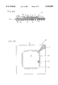
- FIG. 3D is a plan view illustrating the carrier frame 10 which is used in the fourth, fifth and sixth embodiments of the present invention to improve the electrical performance and heat discharge performance of packages.
- the heat discharge plate 11 is formed at the central portion of the carrier frame 10.
- Tie bars 13 are formed at four corners of the heat discharge plate 11.
- the outer support plate 16, which has a square rim shape, is arranged around the heat discharge plate 11 in such a manner that it is connected with the outer ends of the tie bars 13.
- a plurality of openings 14 are formed between the heat discharge plate 11 and outer support plate 16.
- FIGS. 4A and 4B illustrate a BGA semiconductor package using a carrier frame 10 configured in accordance with a seventh embodiment of the present invention, respectively.
- the carrier frame 10 of this embodiment has openings 14 which have a slot shape. These openings 14 are formed only in a region where the circuit pattern 21 on the flexible circuit board is wire-bonded to input/output pads 52 of the semiconductor chip 51. This configuration is adapted to further improve the electrical performance and heat discharge performance of the package.
- FIGS. 5A to 5D are sectional views and plan views respectively illustrating BGA semiconductor packages respectively using carrier frames 10 configured to improve the bonding force between the encapsulate 40 and other constituting elements of the BGA semiconductor packages in accordance with eighth and ninth embodiments of the present invention.
- a plurality of slots 15 are formed in the carrier frame 10 in accordance with the eighth or ninth embodiment.
- the bonding area between the encapsulate 40 and outer support plate 16 increases as shown in FIG. 5A or 5B.
- the slots have a wave shape.
- FIGS. 6A to 6D are sectional views and plan views respectively illustrating BGA semiconductor packages respectively using carrier frames 10 configured to improve the bonding force between the encapsulate 40 and other constituting elements of the BGA semiconductor packages in accordance with tenth and eleventh embodiments of the present invention. These embodiments are similar to the eighth and ninth embodiments.
- the carrier frame 10 of the tenth or eleventh embodiment which includes a heat discharge plate 11 as well as an outer support plate 16, has a plurality of slots 15 formed in the outer support plate 16.
- the slots 15 have a wave shape. That is, the slots 15, may have various shapes such as a slot shape or a wave shape.
- FIG. 7 illustrates a flexible circuit board which is used as a constituting element in all the above-mentioned embodiments of the present invention.
- the flexible circuit board which is denoted by the reference numeral 20, includes a circuit pattern 21 formed only on the upper surface of a flexible resin film 22.
- a plurality of solder ball lands 23 are formed on the lower surface of the flexible resin film 22 in such a manner that they are downwardly exposed.
- the solder ball lands 23 are connected to the circuit pattern 21.
- the formation of the flexible circuit board 20 is achieved by forming a copper thin film over the flexible resin film 22, which is made of a polymer resin, patterning the copper thin film, thereby forming the circuit pattern 21, and then forming a plurality of solder ball lands 23 on the flexible resin film 22 in such a manner that they are connected to the circuit pattern 21 while being downwardly exposed.
- FIG. 8 illustrates the procedure of bonding the carrier frame 10 to the flexible circuit board 20 in the fabrication of the BGA semiconductor package 50 using the flexible circuit board.
- the flexible circuit board 20, adhesive means 60 and carrier frame 10 are laid, in this order, on a lower flat plate 70 laid on a jig 80 such that they are interposed between the lower flat plate and an upper flat plate 84.
- These elements are aligned together as they are coupled to pins 83 upwardly protruded from the jig 80. Under this condition, pressure is applied to the upper flat plate 84 to bond the carrier frame 10 to the flexible circuit board 20.
- FIGS. 9A to 9G are sectional views respectively illustrating sequential steps of a method for fabricating a BGA semiconductor package using the flexible circuit board, to which the carrier frame is bonded as mentioned above, in accordance with the present invention.
- the procedure of bonding the carrier frame to the flexible circuit board and the procedure of fabricating the BGA semiconductor package are carried out in a continuous manner.
- the method of the present invention involves a semiconductor chip bonding step (FIG. 9A), a wire bonding step (FIG. 9B), an encapsulating step (FIG. 9C), a solder ball fusing step (FIG. 9D), and a cutting step (FIG. 9E).
- the flexible circuit board 20 shown in FIG. 7 has a flexible resin film 22 and a circuit pattern 21 comprised of a single copper thin film formed on the flexible resin film 22.
- a plurality of solder ball lands 23 are formed on the lower surface of the flexible resin film 22 in such a manner that they are connected to the circuit pattern 21 while being outwardly exposed.
- the circuit pattern 21 is further comprised of a nickel (Ni) layer (not shown) and a gold (Au) layer (not shown) sequentially plated on the copper thin film.
- the flexible circuit board 20 is centrally defined with a region where a die paddle 25 is formed.
- a semiconductor chip which will be described hereinafter, is directly bonded on the die paddle 25.
- the heat discharge plate of a carrier frame is bonded to the die paddle 25 by an adhesive means.
- the flexible resin film 22 has a thickness ranging from 20 microns to 150 microns. Where the flexible resin film 22 has a thickness of less than 20 microns, it may be broken in the process of the package fabrication. Where the flexible resin film 22 has a thickness of more than 150 microns, an increase in thermal resistivity occurs.
- FIG. 3D shows a typical configuration of the carrier frame 10 adapted to easily discharge heat from the semiconductor chip and to reduce the inductance and capacitance of the circuit pattern while absorbing the coupling effect of the circuit pattern, thereby improving the heat discharge performance and electrical performance.
- the carrier frame 10 has, at the central portion thereof, a square heat discharge plate 11 on which the semiconductor chip is mounted by an adhesive means. Tie bars 13 are formed at four corners of the heat discharge plate 11.
- the carrier frame 10 also has an outer support plate 16 shaped into a square rim and arranged around the heat discharge plate 11 in such a manner that it is connected with the outer ends of the tie bars 13.
- a plurality of openings 14 having a trapezoidal shape are formed between the heat discharge plate 11 and outer support plate 16.
- the openings 14 may have various shapes.
- the 14 may have a slot shape, as shown in FIG. 4B (seventh embodiment).
- the heat discharge plate 11 may be removed to improve the bonding force between the carrier frame 10 and other constituting elements of the BGA semiconductor packages, thereby removing a bending phenomenon of the package, as shown in FIG. 5C and 5D (eight and ninth embodiments).
- a central opening 12 is provided at the carrier frame 10.
- the outer support plate 16 may have a plurality of slots 15 which have a slot shape or a wave shape.
- the heat discharge plate 11 may be left under the condition in which the size of the openings 14 is reduced, as shown in FIGS. 6C and 6D (tenth and eleventh embodiments). In this case, the size of the slots 15 formed at the outer support plate 16 increases.
- the first and slots 14 and 15 may have various shapes.
- the reference character C denotes a cutting line along which the carrier frame is cut by a cutting means in the process of the package fabrication.
- the carrier frame 10 is subjected to a surface treatment, for example, an oxidization (not shown) using an etchant solution, at its surface portion which will be subsequently encapsulated by an encapsulate, in order to maximize the bonding force to the encapsulate.
- Ground bonding regions 18 are formed on the tie bars 13 of the carrier frame 10 using silver (Ag) and palladium (Pd) so as to achieve a good ground bonding between the tie bars 13 and the input/output pads of the semiconductor chip which will be subsequently carried out.
- Silver and palladium are plated on a selected one of the tie bars 13 and a portion of the outer support plate 16 straightly extending from the selected tie bar 13, thereby forming a molding gate 17.
- the outer support plate 16 or heat discharge plate 11 may also have ground bonding regions 18, as in the tie bars 13.
- the shape and size of the ground bonding regions 18 are optional.
- the carrier frame 10 may be made of any material in so far as the material exhibits superior thermal conductivity. Preferably, copper (Cu), copper alloy, aluminum (Al) or stainless steel may be used.
- the carrier frame 10, which have constituting elements such as the heat discharge plate 11, tie bars 13 and outer support plate 16, may be fabricated using a chemical etching method or a stamping method. In the stamping method, a press is used.
- a semiconductor chip 51 which has a plurality of input/output pads 52 at the upper surface thereof.
- the circuit pattern 21 of the flexible circuit board 20 is bonded to the input/output pads 52 of the semiconductor chip 51 by conductive wires 53, respectively.
- the semiconductor chip 51 and conductive wires 53 are encapsulated by an encapsulate 40 in order to protect them from various outside contaminant or mechanical impact.
- a plurality of solder balls 30 are fused as input/output terminals on the lower surface of the flexible circuit board 20.
- An outer support plate 16 which is included in the carrier frame 10 provided for the support and easy handling of constituting elements of a package, is bonded to the outer edge portion of the upper surface of the flexible circuit board 20 by the adhesive means 60 while being in contact with the outer edge of an encapsulate 40.
- the adhesive means 60 comprises an epoxy when it is used to bond the semiconductor chip 51.
- the adhesive means comprises a polyimide tape.
- other adhesive means may be used.
- the electrical connection between the flexible circuit board 20 and the semiconductor chip 51 laid on the flexible circuit board 20 is achieved by wire-bonding ends of the circuit pattern 21 formed on the flexible circuit board 20 to the input/output pads 52 formed on the semiconductor chip 51 using conductive wires 53, respectively.
- the conductive wires 53 are comprised of gold wires or aluminum wires.
- the semiconductor chip 51, the conductive wires 53 and the circuit pattern 21 of flexible circuit board 20 are sensitive to outside moisture, dust, and various mechanical impact or vibrations, they are encapsulated by the encapsulate 40 so that they are protected.
- the encapsulate 40 comprises a liquid epoxy or an epoxy molding compound.
- the molding gate 17, which is described in conjunction with the carrier frame 10, is provided to obtain an advantage in the package fabrication.
- solder balls 30 which are made of an alloy of tin (Sn) and lead (Pb), are fused on solder ball lands 23 defined on the lower surface of the flexible circuit board 20 in a high temperature environment.
- the solder balls 30 are used as input/output means to a main board.
- the outer support plate 16 of the carrier frame 10 serves to maintain the flexible circuit board 20 in a rigid state so as to obtain an easy handling of the flexible circuit board 20 in the package fabrication.
- the outer support plate 16 serves to improve the heat discharge performance.
- the carrier frame 10, which is used in the first embodiment of the present invention, is free of the heat discharge plate 11 and tie bars 13, so that an opening 12 is defined at the central portion of the carrier frame 10. That is, this carrier frame 10 has only the outer support plate 16.
- the outer support plate 16 of the carrier frame 10 is cut by a cutting means (not shown) so that an encapsulate 40 is formed on a region inwardly spaced from the outer edge of the flexible circuit board 20 by a desired distance.
- This package structure is obtained by removing the outer support plate 16 of the carrier frame 10 from the finally obtained package after using it in the process of the package fabrication.
- the carrier frame can be repeatedly used.
- the selection of such a package structure is optional. That is, where the user does not want to use the outer support plate 16, this outer support plate 16 is cut from the carrier frame 10 using a cutting means.
- the portion of the flexible circuit substrate 20, to which the outer support plate 16 is bonded may be removed using the cutting means in the process of the package fabrication, as in the third embodiment of the present invention shown in FIG. 2C.
- the use of conductive via holes and solder masks is eliminated. The elimination of such elements is an objective of the present invention.
- a flexible circuit board is used which has a thickness of 20 to 150 microns and is formed at only one surface thereof with a circuit pattern having a small length. Accordingly, a thin and light package structure is obtained in accordance with those embodiments.
- a carrier frame 10, which comprises a heat discharge plate 11, tie bars 13 and an outer support plate 16, may be used, as in the fourth embodiment of the present invention shown in FIG. 3A.
- the carrier frame 10 is bonded between the flexible circuit board 20 and semiconductor chip 51 by an adhesive means 60.
- the carrier frame 10 may have a configuration in which the outer support plate 16 is removed using a cutting means, as in the fifth embodiment of the present invention shown in FIG. 3B.
- the carrier frame 10 may also have a configuration in which the portion of the flexible circuit substrate 20, to which the outer support plate 16 is bonded, is removed using the cutting means, in addition to the outer support plate 16, as in the sixth embodiment of the present invention shown in FIG. 3C.
- the fourth, fifth and sixth embodiments are adapted to achieve an easy handling of the flexible circuit board 20 in the process of the package fabrication by the outer support plate 16 of the carrier frame 10 disposed on the outer edge portion of the flexible circuit board 20.
- the heat discharge plate 11 of the carrier frame 10 is disposed beneath the semiconductor chip 51, so that heat from the semiconductor chip 51 is easily outwardly discharged. Accordingly, an improvement in the electrical performance and heat discharge performance is achieved.
- openings 14 having a slot shape may be formed in a region only where the circuit pattern 21 on the flexible circuit board 20 is wire-bonded to input/output pads 52 of the semiconductor chip 51, as in the seventh embodiment of the present invention shown in FIGS. 4A and 4B. In this configuration, the area of the carrier frame 10 increases.
- a plurality of slots 15 may also be formed at a portion of the carrier frame 10 inside the outer support plate 16 to improve the bonding force to the encapsulate 40, as in the eighth, ninth, tenth and eleventh embodiments of the present invention shown in FIGS. 5A to 6D.
- the bonding area to the encapsulate 40 increases, thereby obtaining an improvement in the bonding force. Accordingly, it is possible to prevent a bending phenomenon of the BGA semiconductor package mounted on the main board due to heat generated during the operation of the package. That is, these embodiments are adapted to eliminate a bending phenomenon of the package by additionally forming a plurality of slots 15 in the carrier frame 10, thereby improving the bonding force between the encapsulate 40 and other constituting elements of the package.
- a carrier frame which has various shapes, may be used under the condition in which it is bonded to the flexible circuit board 20 by the adhesive means 60. After the completion of the package fabrication, a desired portion of the used carrier frame may be cut out, if necessary.
- the semiconductor chip 51 may be directly bonded to the upper surface of the die paddle 25 formed at the central portion of the flexible circuit board 20 by the adhesive means 60, as shown in FIGS. 2A to 2C and FIGS. 5A and 5B.
- the semiconductor chip 51 may be bonded to the upper surface of the die paddle 25 of the flexible circuit board 20 by the adhesive means 60 in such a manner that the heat discharge plate 11 of the carrier frame 10 is interposed between the die paddle 25 and semiconductor chip 51, as shown in FIGS. 3A to 3C, FIG. 4A and FIGS. 6A and 6B.
- a polyimide tape or epoxy exhibiting a high thermal conductivity is used as the adhesive means 60 so that heat from the semiconductor chip 51 is well transferred to the heat discharge plate 11 of the carrier frame 10.
- FIG. 8 illustrates the procedure of bonding the carrier frame 10 to the flexible circuit board 20.
- the element shown in the uppermost portion of the drawing is the carrier frame
- the element shown in the second upper portion of the drawing is the adhesive means 60
- the third upper portion of the drawing is the flexible circuit board 20.
- the reference numerals 70 and 84 denote a lower flat plate and an upper flat plate, respectively.
- the flexible circuit board 20 comprises circuit patterns 21 which are formed on the flexible resin film 22 using a well-known pattern forming method.
- the flexible circuit board 20 also comprises pin holes 20b.
- the flexible circuit board 20 may have a strip shape or a reel shape.
- the flexible circuit board 20 may also have the form of individual units.
- the adhesive means 60 includes pin holes 60b and openings 62 which correspond to the pin holes 20b and circuit patterns 21 of the flexible circuit board 20, respectively.
- the carrier frame 10 includes pin holes lob and openings 12 which correspond to the pin holes 20b and circuit patterns 21 of the flexible circuit board 20, respectively.
- the carrier frame 10 also includes guide holes 10a adapted to achieve an easy feeding and positioning of the carrier frame.
- the upper and lower flat plates 84 and 70 only have pin holes 70b.
- the element shown in the lowermost portion of FIG. 8 is the jig 80.
- the lower flat plate 70, flexible circuit board 20, adhesive means 60, carrier frame 10 and upper flat plate 84 are laid, in this order, on the jig 80 in such a manner that pins 83 upwardly protruded from the jig 80 pass through associated pin holes of the elements laid on the jig 80. Thereafter, the elements laid on the jig 80 are clamped. Under this condition, pressure is applied to the upper flat plate 84 to bond the carrier frame 10 to the flexible circuit board 20 by the adhesive means 60. Since the circuit pattern 21 is shielded from the outside by the adhesive means 60, it is unnecessary to additionally form a solder mask as in the conventional case.
- FIGS. 9A to 9G are sectional views respectively illustrating sequential steps of a method for fabricating a BGA semiconductor package using the flexible circuit board 20, to which the carrier frame 10 is bonded as mentioned above, in accordance with the present invention.
- this method will now be described in conjunction with the case in which a flexible circuit board associated with one of the first, second and third embodiments of the present invention is used.
- the carrier frame 10 which comprises a heat discharge plate 11 and an outer support plate 16 is first bonded to the flexible circuit board 20 having a circuit pattern 21 formed on its flexible resin film 22, by an adhesive means 60. Thereafter, a semiconductor chip 51 is bonded to the heat discharge plate 11 using an adhesive means 60 (FIG. 9A).
- circuit pattern 21 of the flexible circuit board 20 is wire-bonded to the semiconductor chip 51 by conductive wires 53 such as gold wires or aluminum wires (FIG. 9B).
- the semiconductor chip 51 and conductive wires 53 are then encapsulated by an encapsulate 40 such as an epoxy molding compound or glob top in order to protect them from the environment (FIG. 9C).
- an encapsulate 40 such as an epoxy molding compound or glob top in order to protect them from the environment (FIG. 9C).
- the carrier frame 10 and flexible circuit board 20 have a strip shape to fabricate a plurality of packages in a simultaneous manner. Accordingly, the fabricated packages are cut into individual ones using a cutting means.
- the cutting of the packages may be carried out in such a manner that the outer support plate 16 of the carrier frame 20 in each package is left while being bonded to the outer edge portion of the upper surface of the flexible circuit board 20, as shown in FIG. 9E.
- the cutting of the packages may be carried out in such a manner that the outer support plate 16 of the carrier frame 20 in each package is removed while the outer edge portion of the flexible circuit board 20 protrudes outwardly beyond the outer edge of the encapsulate 40, as shown in FIG. 9F.
- the cutting of the packages may also be carried out in such a manner that in addition to the outer support plate 16, the portion of the flexible circuit substrate 20, to which the outer support plate 16 is bonded, is removed.
- the package fabrication method of the present invention has been described in conjunction with the carrier frame which comprises only the outer support plate 16, it can also be applied to the case in which the carrier frame further comprises the heat discharge plate 11 and tie bars 13. In the latter case, the method requires only a slight modification thereof which is easily appreciable by those skilled in the art.
- This method is also used in the case in which the carrier frame further comprises a plurality of slots 15 formed in the outer support plate 16 thereof. In this case, it is only additionally required to cut portions of the outer support plate 16, where the slots 15 are formed, in such a manner that the outer support plate 16 is partially disposed within the encapsulate 40.
- the BGA semiconductor package fabricated using the flexible circuit board according to the present invention mainly provides the following three effects.
- the package has a thin and light structure because it is fabricated using the flexible circuit board which has no conductive via holes nor solder mask while having a thin structure formed at only one surface thereof with a circuit pattern having a small length.
- an easy handling of the flexible circuit board is achieved because a metallic carrier frame is mounted on the flexible circuit board. It is also possible to achieve a reduction in the inductance, impedance and coupling effect of adjacent circuit patterns, thereby achieving an improvement in electrical performance. In addition, heat from a semiconductor chip is easily outwardly discharged, thereby achieving an improvement in the electrical performance and heat discharge performance.
- the bonding force between the encapsulate and constituting elements of the package increases because the carrier frame has a plurality of openings. Accordingly, it is possible to eliminate a bending phenomenon of the package.
Abstract
Description
Claims (20)
Applications Claiming Priority (6)
| Application Number | Priority Date | Filing Date | Title |
|---|---|---|---|
| KR1019960077898A KR100218633B1 (en) | 1996-12-30 | 1996-12-30 | Ball grid array package having a carrier frame |
| KR96-77899 | 1996-12-30 | ||
| KR96-77898 | 1996-12-30 | ||
| KR1019960077899A KR100218634B1 (en) | 1996-12-30 | 1996-12-30 | Bga package having a carrier frame |
| KR1019970004430A KR100239387B1 (en) | 1997-02-14 | 1997-02-14 | Ball grid array semiconductor package and the manufacture method |
| KR97-4430 | 1997-02-14 |
Publications (1)
| Publication Number | Publication Date |
|---|---|
| US5953589A true US5953589A (en) | 1999-09-14 |
Family
ID=27349455
Family Applications (1)
| Application Number | Title | Priority Date | Filing Date |
|---|---|---|---|
| US08/915,077 Expired - Lifetime US5953589A (en) | 1996-12-30 | 1997-08-20 | Ball grid array semiconductor package with solder balls fused on printed circuit board and method for fabricating the same |
Country Status (2)
| Country | Link |
|---|---|
| US (1) | US5953589A (en) |
| JP (1) | JP3032964B2 (en) |
Cited By (56)
| Publication number | Priority date | Publication date | Assignee | Title |
|---|---|---|---|---|
| US6120885A (en) * | 1997-07-10 | 2000-09-19 | International Business Machines Corporation | Structure, materials, and methods for socketable ball grid |
| US6273327B1 (en) * | 1999-06-16 | 2001-08-14 | Trw Inc. | Apparatus and method for depositing solder material onto a circuit board |
| US6291260B1 (en) * | 2000-01-13 | 2001-09-18 | Siliconware Precision Industries Co., Ltd. | Crack-preventive substrate and process for fabricating solder mask |
| US6297559B1 (en) | 1997-07-10 | 2001-10-02 | International Business Machines Corporation | Structure, materials, and applications of ball grid array interconnections |
| US6337522B1 (en) | 1997-07-10 | 2002-01-08 | International Business Machines Corporation | Structure employing electrically conductive adhesives |
| US6344401B1 (en) * | 2000-03-09 | 2002-02-05 | Atmel Corporation | Method of forming a stacked-die integrated circuit chip package on a water level |
| WO2002045164A2 (en) * | 2000-12-01 | 2002-06-06 | Broadcom Corporation | Thermally and electrically enhanced ball grid array packaging |
| WO2002052645A2 (en) * | 2000-12-22 | 2002-07-04 | Broadcom Corporation | Enhanced die-up ball grid array packages and method for making the same |
| US6455348B1 (en) * | 1998-03-12 | 2002-09-24 | Matsushita Electric Industrial Co., Ltd. | Lead frame, resin-molded semiconductor device, and method for manufacturing the same |
| US20020185722A1 (en) * | 2000-12-22 | 2002-12-12 | Zhao Sam Ziqun | Die-up ball grid array package with enhanced stiffener |
| US20030057550A1 (en) * | 2000-12-22 | 2003-03-27 | Broadcom Corporation | Ball grid array package enhanced with a thermal and electrical connector |
| US20030104657A1 (en) * | 2001-04-05 | 2003-06-05 | Larry Kinsman | Transfer mold semiconductor packaging processes |
| US20030111726A1 (en) * | 2001-12-18 | 2003-06-19 | Khan Reza-Ur Rahman | Ball grid array package substrates and method of making the same |
| EP1333490A2 (en) | 2002-02-01 | 2003-08-06 | Broadcom Corporation | Ball grid array package with patterned stiffener layer |
| US20030146506A1 (en) * | 2002-02-01 | 2003-08-07 | Broadcom Corporation | Ball grid array package fabrication with IC die support structures |
| US20030146503A1 (en) * | 2002-02-01 | 2003-08-07 | Broadcom Corporation | Ball grid array package with stepped stiffener layer |
| US20030146511A1 (en) * | 2002-02-01 | 2003-08-07 | Broadcom Corporation | Ball grid array package with multiple interposers |
| US20030179549A1 (en) * | 2002-03-22 | 2003-09-25 | Zhong Chong Hua | Low voltage drop and high thermal perfor mance ball grid array package |
| US20030179556A1 (en) * | 2002-03-21 | 2003-09-25 | Broadcom Corporation | Enhanced die-up ball grid array package with two substrates and method for making the same |
| US6750533B2 (en) * | 2002-04-10 | 2004-06-15 | Siliconware Precision Industries Co., Ltd. | Substrate with dam bar structure for smooth flow of encapsulating resin |
| US20040154529A1 (en) * | 2003-02-07 | 2004-08-12 | Tatsuki Nogiwa | Substrate holder, method for producing substrate holder, and method for producing mold |
| US6838315B2 (en) * | 2000-08-30 | 2005-01-04 | Renesas Technology Corporation | Semiconductor device manufacturing method wherein electrode members are exposed from a mounting surface of a resin encapsulator |
| DE10323296A1 (en) * | 2003-05-21 | 2005-01-05 | Infineon Technologies Ag | Arrangement for stress reduction for substrate-based chip packages has uniform trench-shaped structures on chip side of substrate to interrupt or displace thermally induced mechanical stress |
| US20050012203A1 (en) * | 2001-02-15 | 2005-01-20 | Rahman Khan Reza-Ur | Enhanced die-down ball grid array and method for making the same |
| US20050022378A1 (en) * | 2001-06-11 | 2005-02-03 | Bolken Todd O. | Apparatus used to package multimedia card by transfer molding |
| US6861760B2 (en) * | 1997-10-06 | 2005-03-01 | Rohm Co., Ltd. | Semiconductor device with stacked-semiconductor chips and support plate |
| US20050133890A1 (en) * | 2003-12-19 | 2005-06-23 | Virgil Liao | Substrate structure capable of reducing package singular stress |
| US20050263886A1 (en) * | 2004-05-28 | 2005-12-01 | Nokia Corporation | Integrated circuit package with optimized mold shape |
| US20050280141A1 (en) * | 2004-06-21 | 2005-12-22 | Broadcom Corporation | Integrated circuit device package having both wire bond and flip-chip interconnections and method of making the same |
| WO2006012167A1 (en) * | 2004-06-25 | 2006-02-02 | Intel Corporation | Bottom heat spreader |
| US20060266545A1 (en) * | 2005-05-24 | 2006-11-30 | Nitto Denko Corporation | Wired circuit board |
| US7169643B1 (en) * | 1998-12-28 | 2007-01-30 | Seiko Epson Corporation | Semiconductor device, method of fabricating the same, circuit board, and electronic apparatus |
| KR100716871B1 (en) * | 2001-04-11 | 2007-05-09 | 앰코 테크놀로지 코리아 주식회사 | Carrier frame for semiconductor package and semiconductor package using it and its manufacturing method |
| US7259448B2 (en) | 2001-05-07 | 2007-08-21 | Broadcom Corporation | Die-up ball grid array package with a heat spreader and method for making the same |
| US20080013594A1 (en) * | 2005-02-25 | 2008-01-17 | 3M Innovative Properties Company | Nondestructive Inspection Method For Inspecting Junction Of Flexible Printed Circuit Board |
| US7432586B2 (en) | 2004-06-21 | 2008-10-07 | Broadcom Corporation | Apparatus and method for thermal and electromagnetic interference (EMI) shielding enhancement in die-up array packages |
| US7482686B2 (en) | 2004-06-21 | 2009-01-27 | Braodcom Corporation | Multipiece apparatus for thermal and electromagnetic interference (EMI) shielding enhancement in die-up array packages and method of making the same |
| US7550845B2 (en) | 2002-02-01 | 2009-06-23 | Broadcom Corporation | Ball grid array package with separated stiffener layer |
| US20100096166A1 (en) * | 2008-10-17 | 2010-04-22 | Occam Portfolio Llc | Flexible Circuit Assemblies without Solder and Methods for their Manufacture |
| US7786591B2 (en) | 2004-09-29 | 2010-08-31 | Broadcom Corporation | Die down ball grid array package |
| US20100284158A1 (en) * | 2009-05-06 | 2010-11-11 | Sehat Sutardja | Packaging techniques and configurations |
| US20100320581A1 (en) * | 2007-03-30 | 2010-12-23 | Oki Semiconductor Co., Ltd. | Semiconductor device |
| US20110156227A1 (en) * | 2009-12-31 | 2011-06-30 | Siliconware Precision Industries Co., Ltd. | Semiconductor package structure |
| US20110182042A1 (en) * | 2007-07-05 | 2011-07-28 | Occam Portfolio Llc | Electronic Assemblies without Solder and Methods for their Manufacture |
| US8183680B2 (en) | 2006-05-16 | 2012-05-22 | Broadcom Corporation | No-lead IC packages having integrated heat spreader for electromagnetic interference (EMI) shielding and thermal enhancement |
| US8338828B2 (en) | 2010-08-05 | 2012-12-25 | Freescale Semiconductor, Inc. | Semiconductor package and method of testing same |
| CN103117260A (en) * | 2011-11-16 | 2013-05-22 | 复旦大学 | Welding spot structure |
| CN103295994A (en) * | 2012-02-29 | 2013-09-11 | 矽品精密工业股份有限公司 | Packaging structure, substrate structure and manufacturing method thereof |
| CN103779286A (en) * | 2014-01-26 | 2014-05-07 | 清华大学 | Encapsulation structure, encapsulation method and template used in encapsulation method |
| CN103794576A (en) * | 2014-01-26 | 2014-05-14 | 清华大学 | Packaging structure and packaging method |
| CN104183509A (en) * | 2013-05-24 | 2014-12-03 | 矽品精密工业股份有限公司 | Method for manufacturing semiconductor package |
| US20160013122A1 (en) * | 2010-04-27 | 2016-01-14 | Aptos Technology Inc. | Methods of fabricating qfn semiconductor package and metal plate |
| EP3662507A4 (en) * | 2017-08-03 | 2021-09-29 | General Electric Company | Electronics package with integrated interconnect structure and method of manufacturing thereof |
| US20210407821A1 (en) * | 2020-06-24 | 2021-12-30 | Samsung Electronics Co., Ltd. | Semiconductor package and method of manufacturing semiconductor package |
| FR3116944A1 (en) * | 2020-12-02 | 2022-06-03 | Stmicroelectronics (Grenoble 2) Sas | INTEGRATED CIRCUIT BOX |
| US20220238472A1 (en) * | 2019-05-21 | 2022-07-28 | Pragmatic Printing Ltd. | Flexible electronic structure |
Families Citing this family (2)
| Publication number | Priority date | Publication date | Assignee | Title |
|---|---|---|---|---|
| KR100474193B1 (en) * | 1997-08-11 | 2005-07-21 | 삼성전자주식회사 | BG Package and Manufacturing Method |
| JP2000208905A (en) * | 1999-01-14 | 2000-07-28 | Nec Corp | Printed board |
Citations (3)
| Publication number | Priority date | Publication date | Assignee | Title |
|---|---|---|---|---|
| US5216278A (en) * | 1990-12-04 | 1993-06-01 | Motorola, Inc. | Semiconductor device having a pad array carrier package |
| US5620928A (en) * | 1995-05-11 | 1997-04-15 | National Semiconductor Corporation | Ultra thin ball grid array using a flex tape or printed wiring board substrate and method |
| US5793118A (en) * | 1994-05-26 | 1998-08-11 | Nec Corporation | Semiconductor device capable of accomplishing a high moisture proof |
-
1997
- 1997-08-14 JP JP9233372A patent/JP3032964B2/en not_active Expired - Fee Related
- 1997-08-20 US US08/915,077 patent/US5953589A/en not_active Expired - Lifetime
Patent Citations (3)
| Publication number | Priority date | Publication date | Assignee | Title |
|---|---|---|---|---|
| US5216278A (en) * | 1990-12-04 | 1993-06-01 | Motorola, Inc. | Semiconductor device having a pad array carrier package |
| US5793118A (en) * | 1994-05-26 | 1998-08-11 | Nec Corporation | Semiconductor device capable of accomplishing a high moisture proof |
| US5620928A (en) * | 1995-05-11 | 1997-04-15 | National Semiconductor Corporation | Ultra thin ball grid array using a flex tape or printed wiring board substrate and method |
Cited By (138)
| Publication number | Priority date | Publication date | Assignee | Title |
|---|---|---|---|---|
| US6297559B1 (en) | 1997-07-10 | 2001-10-02 | International Business Machines Corporation | Structure, materials, and applications of ball grid array interconnections |
| US6300164B1 (en) | 1997-07-10 | 2001-10-09 | International Business Machines Corporation | Structure, materials, and methods for socketable ball grid |
| US6337522B1 (en) | 1997-07-10 | 2002-01-08 | International Business Machines Corporation | Structure employing electrically conductive adhesives |
| US6120885A (en) * | 1997-07-10 | 2000-09-19 | International Business Machines Corporation | Structure, materials, and methods for socketable ball grid |
| US7242100B2 (en) | 1997-10-06 | 2007-07-10 | Rohm Co., Ltd. | Method for manufacturing semiconductor device with plural semiconductor chips |
| US6861760B2 (en) * | 1997-10-06 | 2005-03-01 | Rohm Co., Ltd. | Semiconductor device with stacked-semiconductor chips and support plate |
| US20050153480A1 (en) * | 1997-10-06 | 2005-07-14 | Rohm Co., Ltd. | Semiconductor device and method for making the same |
| US6455348B1 (en) * | 1998-03-12 | 2002-09-24 | Matsushita Electric Industrial Co., Ltd. | Lead frame, resin-molded semiconductor device, and method for manufacturing the same |
| US7169643B1 (en) * | 1998-12-28 | 2007-01-30 | Seiko Epson Corporation | Semiconductor device, method of fabricating the same, circuit board, and electronic apparatus |
| US6273327B1 (en) * | 1999-06-16 | 2001-08-14 | Trw Inc. | Apparatus and method for depositing solder material onto a circuit board |
| US6291260B1 (en) * | 2000-01-13 | 2001-09-18 | Siliconware Precision Industries Co., Ltd. | Crack-preventive substrate and process for fabricating solder mask |
| US6344401B1 (en) * | 2000-03-09 | 2002-02-05 | Atmel Corporation | Method of forming a stacked-die integrated circuit chip package on a water level |
| US6838315B2 (en) * | 2000-08-30 | 2005-01-04 | Renesas Technology Corporation | Semiconductor device manufacturing method wherein electrode members are exposed from a mounting surface of a resin encapsulator |
| US6882042B2 (en) | 2000-12-01 | 2005-04-19 | Broadcom Corporation | Thermally and electrically enhanced ball grid array packaging |
| US20020135065A1 (en) * | 2000-12-01 | 2002-09-26 | Zhao Sam Ziqun | Thermally and electrically enhanced ball grid array packaging |
| US8686558B2 (en) | 2000-12-01 | 2014-04-01 | Broadcom Corporation | Thermally and electrically enhanced ball grid array package |
| WO2002045164A2 (en) * | 2000-12-01 | 2002-06-06 | Broadcom Corporation | Thermally and electrically enhanced ball grid array packaging |
| WO2002045164A3 (en) * | 2000-12-01 | 2003-03-27 | Broadcom Corp | Thermally and electrically enhanced ball grid array packaging |
| US7629681B2 (en) | 2000-12-01 | 2009-12-08 | Broadcom Corporation | Ball grid array package with patterned stiffener surface and method of assembling the same |
| US8039949B2 (en) | 2000-12-01 | 2011-10-18 | Broadcom Corporation | Ball grid array package having one or more stiffeners |
| US20020190362A1 (en) * | 2000-12-22 | 2002-12-19 | Khan Reza-Ur R. | Die-up ball grid array package with patterned stiffener opening |
| US7132744B2 (en) | 2000-12-22 | 2006-11-07 | Broadcom Corporation | Enhanced die-up ball grid array packages and method for making the same |
| US8310067B2 (en) | 2000-12-22 | 2012-11-13 | Broadcom Corporation | Ball grid array package enhanced with a thermal and electrical connector |
| US7005737B2 (en) * | 2000-12-22 | 2006-02-28 | Broadcom Corporation | Die-up ball grid array package with enhanced stiffener |
| US7893546B2 (en) | 2000-12-22 | 2011-02-22 | Broadcom Corporation | Ball grid array package enhanced with a thermal and electrical connector |
| US7859101B2 (en) * | 2000-12-22 | 2010-12-28 | Broadcom Corporation | Die-up ball grid array package with die-attached heat spreader |
| WO2002052645A3 (en) * | 2000-12-22 | 2003-05-30 | Broadcom Corp | Enhanced die-up ball grid array packages and method for making the same |
| US7579217B2 (en) | 2000-12-22 | 2009-08-25 | Broadcom Corporation | Methods of making a die-up ball grid array package with printed circuit board attachable heat spreader |
| US7462933B2 (en) | 2000-12-22 | 2008-12-09 | Broadcom Corporation | Ball grid array package enhanced with a thermal and electrical connector |
| US7102225B2 (en) | 2000-12-22 | 2006-09-05 | Broadcom Corporation | Die-up ball grid array package with printed circuit board attachable heat spreader |
| US6989593B2 (en) * | 2000-12-22 | 2006-01-24 | Broadcom Corporation | Die-up ball grid array package with patterned stiffener opening |
| US20020185720A1 (en) * | 2000-12-22 | 2002-12-12 | Khan Reza-Ur R. | Die-up ball grid array package with attached stiffener ring |
| US20040212051A1 (en) * | 2000-12-22 | 2004-10-28 | Broadcom Corporation | Ball grid array package with patterned stiffener layer |
| US20030057550A1 (en) * | 2000-12-22 | 2003-03-27 | Broadcom Corporation | Ball grid array package enhanced with a thermal and electrical connector |
| US20020190361A1 (en) * | 2000-12-22 | 2002-12-19 | Zhao Sam Z. | Die-up ball grid array package with die-attached heat spreader |
| US7161239B2 (en) * | 2000-12-22 | 2007-01-09 | Broadcom Corporation | Ball grid array package enhanced with a thermal and electrical connector |
| WO2002052645A2 (en) * | 2000-12-22 | 2002-07-04 | Broadcom Corporation | Enhanced die-up ball grid array packages and method for making the same |
| US20020185722A1 (en) * | 2000-12-22 | 2002-12-12 | Zhao Sam Ziqun | Die-up ball grid array package with enhanced stiffener |
| US7202559B2 (en) | 2000-12-22 | 2007-04-10 | Broadcom Corporation | Method of assembling a ball grid array package with patterned stiffener layer |
| US6906414B2 (en) | 2000-12-22 | 2005-06-14 | Broadcom Corporation | Ball grid array package with patterned stiffener layer |
| US20050029657A1 (en) * | 2000-12-22 | 2005-02-10 | Broadcom Corporation | Enhanced die-up ball grid array and method for making the same |
| US7038312B2 (en) * | 2000-12-22 | 2006-05-02 | Broadcom Corporation | Die-up ball grid array package with attached stiffener ring |
| US20020185734A1 (en) * | 2000-12-22 | 2002-12-12 | Zhao Sam Ziqun | Die-up ball grid array package with printed circuit board attachable heat spreader |
| US7227256B2 (en) * | 2000-12-22 | 2007-06-05 | Broadcom Corporation | Die-up ball grid array package with printed circuit board attachable heat spreader |
| US7402906B2 (en) | 2001-02-15 | 2008-07-22 | Broadcom Corporation | Enhanced die-down ball grid array and method for making the same |
| US20050012203A1 (en) * | 2001-02-15 | 2005-01-20 | Rahman Khan Reza-Ur | Enhanced die-down ball grid array and method for making the same |
| US6853070B2 (en) | 2001-02-15 | 2005-02-08 | Broadcom Corporation | Die-down ball grid array package with die-attached heat spreader and method for making the same |
| US20050101061A1 (en) * | 2001-04-05 | 2005-05-12 | Larry Kinsman | Transfer mold semiconductor packaging processes, circuit substrates, semiconductor packages, and ball grid arrays |
| US7148083B2 (en) * | 2001-04-05 | 2006-12-12 | Micron Technology, Inc. | Transfer mold semiconductor packaging processes |
| US7384805B2 (en) | 2001-04-05 | 2008-06-10 | Micron Technology, Inc. | Transfer mold semiconductor packaging processes |
| US20030104657A1 (en) * | 2001-04-05 | 2003-06-05 | Larry Kinsman | Transfer mold semiconductor packaging processes |
| KR100716871B1 (en) * | 2001-04-11 | 2007-05-09 | 앰코 테크놀로지 코리아 주식회사 | Carrier frame for semiconductor package and semiconductor package using it and its manufacturing method |
| US7259448B2 (en) | 2001-05-07 | 2007-08-21 | Broadcom Corporation | Die-up ball grid array package with a heat spreader and method for making the same |
| US7259457B2 (en) | 2001-05-07 | 2007-08-21 | Broadcom Corporation | Die-up ball grid array package including a substrate capable of mounting an integrated circuit die and method for making the same |
| US20050022378A1 (en) * | 2001-06-11 | 2005-02-03 | Bolken Todd O. | Apparatus used to package multimedia card by transfer molding |
| US6879039B2 (en) | 2001-12-18 | 2005-04-12 | Broadcom Corporation | Ball grid array package substrates and method of making the same |
| US20030111726A1 (en) * | 2001-12-18 | 2003-06-19 | Khan Reza-Ur Rahman | Ball grid array package substrates and method of making the same |
| US7405145B2 (en) | 2001-12-18 | 2008-07-29 | Broadcom Corporation | Ball grid array package substrates with a modified central opening and method for making the same |
| US6825108B2 (en) | 2002-02-01 | 2004-11-30 | Broadcom Corporation | Ball grid array package fabrication with IC die support structures |
| US7241645B2 (en) | 2002-02-01 | 2007-07-10 | Broadcom Corporation | Method for assembling a ball grid array package with multiple interposers |
| EP1361611A3 (en) * | 2002-02-01 | 2006-04-19 | Broadcom Corporation | Ball grid array package with stepped stiffener layer |
| EP1333491A3 (en) * | 2002-02-01 | 2006-04-19 | Broadcom Corporation | Ball grid array package enhanced with a thermal and electrical connector |
| US7078806B2 (en) | 2002-02-01 | 2006-07-18 | Broadcom Corporation | IC die support structures for ball grid array package fabrication |
| EP1333490A2 (en) | 2002-02-01 | 2003-08-06 | Broadcom Corporation | Ball grid array package with patterned stiffener layer |
| EP1361611A2 (en) * | 2002-02-01 | 2003-11-12 | Broadcom Corporation | Ball grid array package with stepped stiffener layer |
| US20030146506A1 (en) * | 2002-02-01 | 2003-08-07 | Broadcom Corporation | Ball grid array package fabrication with IC die support structures |
| US20030146503A1 (en) * | 2002-02-01 | 2003-08-07 | Broadcom Corporation | Ball grid array package with stepped stiffener layer |
| EP1333490A3 (en) * | 2002-02-01 | 2006-04-19 | Broadcom Corporation | Ball grid array package with patterned stiffener layer |
| US7550845B2 (en) | 2002-02-01 | 2009-06-23 | Broadcom Corporation | Ball grid array package with separated stiffener layer |
| US7245500B2 (en) * | 2002-02-01 | 2007-07-17 | Broadcom Corporation | Ball grid array package with stepped stiffener layer |
| US6861750B2 (en) | 2002-02-01 | 2005-03-01 | Broadcom Corporation | Ball grid array package with multiple interposers |
| US20030146511A1 (en) * | 2002-02-01 | 2003-08-07 | Broadcom Corporation | Ball grid array package with multiple interposers |
| US7312108B2 (en) | 2002-03-21 | 2007-12-25 | Broadcom Corporation | Method for assembling a ball grid array package with two substrates |
| US6887741B2 (en) | 2002-03-21 | 2005-05-03 | Broadcom Corporation | Method for making an enhanced die-up ball grid array package with two substrates |
| US6876553B2 (en) | 2002-03-21 | 2005-04-05 | Broadcom Corporation | Enhanced die-up ball grid array package with two substrates |
| EP1351293A3 (en) * | 2002-03-21 | 2006-11-02 | Broadcom Corporation | Die-up ball grid array package with two substrates and method for making the same |
| EP1351293A2 (en) * | 2002-03-21 | 2003-10-08 | Broadcom Corporation | Die-up ball grid array package with two substrates and method for making the same |
| US20040113284A1 (en) * | 2002-03-21 | 2004-06-17 | Broadcom Corporation | Method for making an enhanced die-up ball grid array package with two substrates |
| US20030179556A1 (en) * | 2002-03-21 | 2003-09-25 | Broadcom Corporation | Enhanced die-up ball grid array package with two substrates and method for making the same |
| US7566590B2 (en) | 2002-03-22 | 2009-07-28 | Broadcom Corporation | Low voltage drop and high thermal performance ball grid array package |
| US7196415B2 (en) | 2002-03-22 | 2007-03-27 | Broadcom Corporation | Low voltage drop and high thermal performance ball grid array package |
| US20030179549A1 (en) * | 2002-03-22 | 2003-09-25 | Zhong Chong Hua | Low voltage drop and high thermal perfor mance ball grid array package |
| US7781882B2 (en) | 2002-03-22 | 2010-08-24 | Broadcom Corporation | Low voltage drop and high thermal performance ball grid array package |
| US6750533B2 (en) * | 2002-04-10 | 2004-06-15 | Siliconware Precision Industries Co., Ltd. | Substrate with dam bar structure for smooth flow of encapsulating resin |
| US20040154529A1 (en) * | 2003-02-07 | 2004-08-12 | Tatsuki Nogiwa | Substrate holder, method for producing substrate holder, and method for producing mold |
| US7180162B2 (en) * | 2003-05-21 | 2007-02-20 | Infineon Technologies Ag | Arrangement for reducing stress in substrate-based chip packages |
| DE10323296A1 (en) * | 2003-05-21 | 2005-01-05 | Infineon Technologies Ag | Arrangement for stress reduction for substrate-based chip packages has uniform trench-shaped structures on chip side of substrate to interrupt or displace thermally induced mechanical stress |
| US20050017354A1 (en) * | 2003-05-21 | 2005-01-27 | Jens Paul | Arrangement for reducing stress in substrate-based chip packages |
| US6933592B2 (en) * | 2003-12-19 | 2005-08-23 | Global Advanced Packaging Technology H.K. Limited | Substrate structure capable of reducing package singular stress |
| US20050133890A1 (en) * | 2003-12-19 | 2005-06-23 | Virgil Liao | Substrate structure capable of reducing package singular stress |
| US20050263886A1 (en) * | 2004-05-28 | 2005-12-01 | Nokia Corporation | Integrated circuit package with optimized mold shape |
| WO2005119767A1 (en) * | 2004-05-28 | 2005-12-15 | Nokia Corporation | Integrated circuit package with optimized mold shape |
| US7233057B2 (en) | 2004-05-28 | 2007-06-19 | Nokia Corporation | Integrated circuit package with optimized mold shape |
| US7595227B2 (en) | 2004-06-21 | 2009-09-29 | Broadcom Corporation | Integrated circuit device package having both wire bond and flip-chip interconnections and method of making the same |
| US7791189B2 (en) | 2004-06-21 | 2010-09-07 | Broadcom Corporation | Multipiece apparatus for thermal and electromagnetic interference (EMI) shielding enhancement in die-up array packages and method of making the same |
| US7432586B2 (en) | 2004-06-21 | 2008-10-07 | Broadcom Corporation | Apparatus and method for thermal and electromagnetic interference (EMI) shielding enhancement in die-up array packages |
| US7411281B2 (en) | 2004-06-21 | 2008-08-12 | Broadcom Corporation | Integrated circuit device package having both wire bond and flip-chip interconnections and method of making the same |
| US20050280141A1 (en) * | 2004-06-21 | 2005-12-22 | Broadcom Corporation | Integrated circuit device package having both wire bond and flip-chip interconnections and method of making the same |
| US7482686B2 (en) | 2004-06-21 | 2009-01-27 | Braodcom Corporation | Multipiece apparatus for thermal and electromagnetic interference (EMI) shielding enhancement in die-up array packages and method of making the same |
| US7190068B2 (en) | 2004-06-25 | 2007-03-13 | Intel Corporation | Bottom heat spreader |
| WO2006012167A1 (en) * | 2004-06-25 | 2006-02-02 | Intel Corporation | Bottom heat spreader |
| US7786591B2 (en) | 2004-09-29 | 2010-08-31 | Broadcom Corporation | Die down ball grid array package |
| US8021927B2 (en) | 2004-09-29 | 2011-09-20 | Broadcom Corporation | Die down ball grid array packages and method for making same |
| US20080013594A1 (en) * | 2005-02-25 | 2008-01-17 | 3M Innovative Properties Company | Nondestructive Inspection Method For Inspecting Junction Of Flexible Printed Circuit Board |
| US7288725B2 (en) * | 2005-05-24 | 2007-10-30 | Nitto Denko Corporation | Wired circuit board |
| EP1727407A3 (en) * | 2005-05-24 | 2008-06-11 | Nitto Denko Corporation | Wired circuit board |
| US20060266545A1 (en) * | 2005-05-24 | 2006-11-30 | Nitto Denko Corporation | Wired circuit board |
| US8183680B2 (en) | 2006-05-16 | 2012-05-22 | Broadcom Corporation | No-lead IC packages having integrated heat spreader for electromagnetic interference (EMI) shielding and thermal enhancement |
| US8432025B2 (en) * | 2007-03-30 | 2013-04-30 | Lapis Semiconductor Co., Ltd. | Semiconductor device and plurality of dams |
| US20100320581A1 (en) * | 2007-03-30 | 2010-12-23 | Oki Semiconductor Co., Ltd. | Semiconductor device |
| US20110182042A1 (en) * | 2007-07-05 | 2011-07-28 | Occam Portfolio Llc | Electronic Assemblies without Solder and Methods for their Manufacture |
| US8193042B2 (en) * | 2008-10-17 | 2012-06-05 | Occam Portfolio Llc | Flexible circuit assemblies without solder and methods for their manufacture |
| US20100096166A1 (en) * | 2008-10-17 | 2010-04-22 | Occam Portfolio Llc | Flexible Circuit Assemblies without Solder and Methods for their Manufacture |
| US8400774B2 (en) * | 2009-05-06 | 2013-03-19 | Marvell World Trade Ltd. | Packaging techniques and configurations |
| US20100284158A1 (en) * | 2009-05-06 | 2010-11-11 | Sehat Sutardja | Packaging techniques and configurations |
| US20130215579A1 (en) * | 2009-05-06 | 2013-08-22 | Marvell World Trade Ltd. | Packaging techniques and configurations |
| US20110156227A1 (en) * | 2009-12-31 | 2011-06-30 | Siliconware Precision Industries Co., Ltd. | Semiconductor package structure |
| US8421199B2 (en) * | 2009-12-31 | 2013-04-16 | Siliconware Precision Industries Co., Ltd. | Semiconductor package structure |
| US8981575B2 (en) | 2009-12-31 | 2015-03-17 | Siliconware Precision Industries Co., Ltd. | Semiconductor package structure |
| US9659842B2 (en) * | 2010-04-27 | 2017-05-23 | Aptos Technology Inc. | Methods of fabricating QFN semiconductor package and metal plate |
| US20160013122A1 (en) * | 2010-04-27 | 2016-01-14 | Aptos Technology Inc. | Methods of fabricating qfn semiconductor package and metal plate |
| US8338828B2 (en) | 2010-08-05 | 2012-12-25 | Freescale Semiconductor, Inc. | Semiconductor package and method of testing same |
| CN103117260A (en) * | 2011-11-16 | 2013-05-22 | 复旦大学 | Welding spot structure |
| CN103295994B (en) * | 2012-02-29 | 2016-02-03 | 矽品精密工业股份有限公司 | packaging structure, substrate structure and manufacturing method thereof |
| CN103295994A (en) * | 2012-02-29 | 2013-09-11 | 矽品精密工业股份有限公司 | Packaging structure, substrate structure and manufacturing method thereof |
| CN104183509A (en) * | 2013-05-24 | 2014-12-03 | 矽品精密工业股份有限公司 | Method for manufacturing semiconductor package |
| CN104183509B (en) * | 2013-05-24 | 2017-11-21 | 矽品精密工业股份有限公司 | Method for manufacturing semiconductor package |
| CN103794576A (en) * | 2014-01-26 | 2014-05-14 | 清华大学 | Packaging structure and packaging method |
| CN103779286A (en) * | 2014-01-26 | 2014-05-07 | 清华大学 | Encapsulation structure, encapsulation method and template used in encapsulation method |
| US9960093B2 (en) | 2014-01-26 | 2018-05-01 | Tsinghua University | Packaging structure, packaging method and template used in packaging method |
| CN109742034A (en) * | 2014-01-26 | 2019-05-10 | 清华大学 | A kind of encapsulating structure, packaging method and the template used in packaging method |
| CN109801846A (en) * | 2014-01-26 | 2019-05-24 | 清华大学 | A kind of encapsulating structure and packaging method |
| EP3662507A4 (en) * | 2017-08-03 | 2021-09-29 | General Electric Company | Electronics package with integrated interconnect structure and method of manufacturing thereof |
| US20220238472A1 (en) * | 2019-05-21 | 2022-07-28 | Pragmatic Printing Ltd. | Flexible electronic structure |
| US20210407821A1 (en) * | 2020-06-24 | 2021-12-30 | Samsung Electronics Co., Ltd. | Semiconductor package and method of manufacturing semiconductor package |
| US11610786B2 (en) * | 2020-06-24 | 2023-03-21 | Samsung Electronics., Co., Ltd. | Semiconductor package and method of manufacturing semiconductor package |
| US11894242B2 (en) | 2020-06-24 | 2024-02-06 | Samsung Electronics Co, Ltd. | Semiconductor package and method of manufacturing semiconductor package |
| FR3116944A1 (en) * | 2020-12-02 | 2022-06-03 | Stmicroelectronics (Grenoble 2) Sas | INTEGRATED CIRCUIT BOX |
Also Published As
| Publication number | Publication date |
|---|---|
| JPH10200012A (en) | 1998-07-31 |
| JP3032964B2 (en) | 2000-04-17 |
Similar Documents
| Publication | Publication Date | Title |
|---|---|---|
| US5953589A (en) | Ball grid array semiconductor package with solder balls fused on printed circuit board and method for fabricating the same | |
| US6228683B1 (en) | High density leaded ball-grid array package | |
| US8278150B2 (en) | Stackable packages for three-dimensional packaging of semiconductor dice | |
| US7087461B2 (en) | Process and lead frame for making leadless semiconductor packages | |
| EP1235272B1 (en) | Leadframe, resin-molded semiconductor device including the leadframe, method of making the leadframe and method for manufacturing the device | |
| KR100294719B1 (en) | Molded semiconductor device and method for manufacturing the same, lead frame | |
| US6664615B1 (en) | Method and apparatus for lead-frame based grid array IC packaging | |
| US7432583B2 (en) | Leadless leadframe package substitute and stack package | |
| US6586834B1 (en) | Die-up tape ball grid array package | |
| US20090309237A1 (en) | Semiconductor package system with substrate having different bondable heights at lead finger tips | |
| US6278177B1 (en) | Substrateless chip scale package and method of making same | |
| US20080308951A1 (en) | Semiconductor package and fabrication method thereof | |
| US20130200507A1 (en) | Two-sided die in a four-sided leadframe based package | |
| KR100292033B1 (en) | Semiconductor chip package and method for manufacturing same | |
| US8349655B2 (en) | Method of fabricating a two-sided die in a four-sided leadframe based package | |
| KR100470144B1 (en) | Semiconductor chip package with tape circuit board and chip size using it | |
| US11869831B2 (en) | Semiconductor package with improved board level reliability | |
| US20010001069A1 (en) | Metal stud array packaging | |
| KR100456482B1 (en) | Bga package using patterned leadframe to reduce fabricating cost as compared with bga package using substrate having stacked multilayered interconnection pattern layer | |
| JPH06132443A (en) | Semiconductor device and lead frame used for manufacture thereof | |
| KR200159861Y1 (en) | Semiconductor package | |
| KR100612761B1 (en) | Chip scale stack chip package | |
| KR100195511B1 (en) | Ball grid array package using leadframe | |
| KR19980083259A (en) | Structure of Chip Size Semiconductor Package and Manufacturing Method Thereof | |
| KR19980015389A (en) | TAB (TAPE AUTOMATED BONDING) LGA (LAND GRID ARRAY) package using support ring |
Legal Events
| Date | Code | Title | Description |
|---|---|---|---|
| AS | Assignment |
Owner name: AMKOR ELECTRONICS, INC., ARIZONA Free format text: ASSIGNMENT OF ASSIGNORS INTEREST;ASSIGNORS:SHIM, II KWON;HEO, YOUNG WOOK;DARVEAUX, ROBERT F.;REEL/FRAME:008767/0249;SIGNING DATES FROM 19970424 TO 19970730 Owner name: ANAM INDUSTRIAL COL, LTD., KOREA, REPUBLIC OF Free format text: ASSIGNMENT OF ASSIGNORS INTEREST;ASSIGNORS:SHIM, II KWON;HEO, YOUNG WOOK;DARVEAUX, ROBERT F.;REEL/FRAME:008767/0249;SIGNING DATES FROM 19970424 TO 19970730 |
|
| AS | Assignment |
Owner name: ANAM SEMICONDUCTOR INC., KOREA, REPUBLIC OF Free format text: MERGER AND CHANGE OF NAME;ASSIGNORS:ANAM INDUSTRIAL CO., LTD.;AMKOR ELECTRONICS, INC.;REEL/FRAME:009424/0605;SIGNING DATES FROM 19980320 TO 19980414 |
|
| AS | Assignment |
Owner name: ANAM SEMICONDUCTOR INC., KOREA, REPUBLIC OF Free format text: CHANGE OF NAME;ASSIGNOR:ANAM INDUSTRIAL CO., LTD.;REEL/FRAME:009962/0222 Effective date: 19980320 Owner name: AMKOR TECHNOLOGY, INC., ARIZONA Free format text: ASSIGNMENT OF ASSIGNORS INTEREST;ASSIGNOR:AMKOR ELECTRONICS, INC.;REEL/FRAME:009962/0247 Effective date: 19980414 |
|
| STCF | Information on status: patent grant |
Free format text: PATENTED CASE |
|
| CC | Certificate of correction | ||
| AS | Assignment |
Owner name: GUARDIAN ASSETS, INC., PENNSYLVANIA Free format text: SECURITY INTEREST;ASSIGNOR:AMKOR TECHNOLOGY, INC.;REEL/FRAME:011122/0773 Effective date: 20000428 |
|
| AS | Assignment |
Owner name: SOCIETE GENERALE, NEW YORK Free format text: RE-RECORD TO CORRECT RECEIVING PARTY NAME ON A DOCUMENT PREVIOUSLY RECORDED ON REEL 011122, FRAME 0773.;ASSIGNORS:AMKOR TECHNOLOGY, INC.;GUARDIAN ASSETS, INC.;REEL/FRAME:011457/0702 Effective date: 20000428 |
|
| AS | Assignment |
Owner name: CITICORP USA, INC., NEW YORK Free format text: SECURITY INTEREST;ASSIGNORS:SOCIETE GENERALE;GUARDIAN ASSETS, INC.;REEL/FRAME:011682/0416 Effective date: 20010330 |
|
| AS | Assignment |
Owner name: AMKOR TECHNOLOGY KOREA, INC., KOREA, REPUBLIC OF Free format text: ASSIGNMENT OF ASSIGNORS INTEREST;ASSIGNOR:ANAM SEMICONDUCTOR, INC.;REEL/FRAME:013193/0683 Effective date: 20000502 |
|
| AS | Assignment |
Owner name: AMKOR TECHNOLOGY, INC., ARIZONA Free format text: ASSIGNMENT OF ASSIGNORS INTEREST;ASSIGNOR:AMKOR TECHNOLOGY KOREA, INC.;REEL/FRAME:013323/0853 Effective date: 20020913 |
|
| FEPP | Fee payment procedure |
Free format text: PAYOR NUMBER ASSIGNED (ORIGINAL EVENT CODE: ASPN); ENTITY STATUS OF PATENT OWNER: LARGE ENTITY |
|
| FPAY | Fee payment |
Year of fee payment: 4 |
|
| AS | Assignment |
Owner name: CITICORP NORTH AMERICA, INC. AS ADMINISTRATIVE AGE Free format text: SECURITY AGREEMENT;ASSIGNORS:AMKOR TECHNOLOGY, INC.;GUARDIAN ASSETS, INC.;REEL/FRAME:014885/0691 Effective date: 20040629 |
|
| AS | Assignment |
Owner name: AMKOR TECHNOLOGY, INC., PENNSYLVANIA Free format text: RELEASE OF LIEN ON PATENTS;ASSIGNOR:CITICORP USA, INC. AS COLLATERAL AGENT;REEL/FRAME:015603/0572 Effective date: 20040629 |
|
| AS | Assignment |
Owner name: CITICORP NORTH AMERICA, INC. AS "AGENT", NEW YORK Free format text: SECURITY AGREEMENT;ASSIGNORS:AMKOR TECHNOLOGY, INC.;GUARDIAN ASSETS, INC.;REEL/FRAME:015942/0521 Effective date: 20041027 |
|
| AS | Assignment |
Owner name: AMKOR TECHNOLOGY, INC., ARIZONA Free format text: TERMINATION & RELEASE OF PATENT SECURITY AGREEMENT;ASSIGNOR:CITICORP NORTH AMERICA, INC.;REEL/FRAME:017388/0868 Effective date: 20051128 Owner name: BANK OF AMERICA, N.A., TEXAS Free format text: SECURITY AGREEMENT;ASSIGNOR:AMKOR TECHNOLOGY, INC.;REEL/FRAME:017379/0630 Effective date: 20051123 |
|
| FPAY | Fee payment |
Year of fee payment: 8 |
|
| FPAY | Fee payment |
Year of fee payment: 12 |
|
| AS | Assignment |
Owner name: BANK OF AMERICA, N.A., AS AGENT, CALIFORNIA Free format text: SECURITY INTEREST;ASSIGNOR:AMKOR TECHNOLOGY, INC.;REEL/FRAME:046683/0139 Effective date: 20180713 |
|
| AS | Assignment |
Owner name: AMKOR TECHNOLOGY SINGAPORE HOLDING PTE.LTD., SINGAPORE Free format text: ASSIGNMENT OF ASSIGNORS INTEREST;ASSIGNOR:AMKOR TECHNOLOGY, INC.;REEL/FRAME:054036/0599 Effective date: 20191119 |