US5953748A - Processor with an efficient translation lookaside buffer which uses previous address computation results - Google Patents
Processor with an efficient translation lookaside buffer which uses previous address computation results Download PDFInfo
- Publication number
- US5953748A US5953748A US08/732,862 US73286296A US5953748A US 5953748 A US5953748 A US 5953748A US 73286296 A US73286296 A US 73286296A US 5953748 A US5953748 A US 5953748A
- Authority
- US
- United States
- Prior art keywords
- memory address
- virtual memory
- translation lookaside
- address
- lookaside buffer
- Prior art date
- Legal status (The legal status is an assumption and is not a legal conclusion. Google has not performed a legal analysis and makes no representation as to the accuracy of the status listed.)
- Expired - Lifetime
Links
Images


Classifications
-
- G—PHYSICS
- G06—COMPUTING; CALCULATING OR COUNTING
- G06F—ELECTRIC DIGITAL DATA PROCESSING
- G06F12/00—Accessing, addressing or allocating within memory systems or architectures
- G06F12/02—Addressing or allocation; Relocation
- G06F12/08—Addressing or allocation; Relocation in hierarchically structured memory systems, e.g. virtual memory systems
- G06F12/10—Address translation
- G06F12/1027—Address translation using associative or pseudo-associative address translation means, e.g. translation look-aside buffer [TLB]
-
- G—PHYSICS
- G06—COMPUTING; CALCULATING OR COUNTING
- G06F—ELECTRIC DIGITAL DATA PROCESSING
- G06F2212/00—Indexing scheme relating to accessing, addressing or allocation within memory systems or architectures
- G06F2212/68—Details of translation look-aside buffer [TLB]
- G06F2212/681—Multi-level TLB, e.g. microTLB and main TLB
Definitions
- the present invention relates to high performance computers; and, in particular, relates to high performance computers providing a large virtual memory space.
- a virtual memory system provides a computer programmer a large conceptual address space which is typically implemented in a much smaller physical address space for practical reasons.
- the physical addresses in the physical address space are used to access physical memory locations in which data or instructions are actually stored.
- the functions and the benefits of a virtual memory system are well-known.
- a page table is used to map a portion of the virtual memory address into a corresponding physical memory page address, which is then used to derive the physical memory address.
- TLB translation look-aside buffer
- a method and a structure provide a translation lookaside buffer (TLB) for translating a virtual memory address to a physical memory address.
- TLB translation lookaside buffer
- the present invention is applicable to a system in which a virtual memory address is computed by adding a base address to an offset value.
- each entry of the TLB is provided a plurality of buffer entry circuits, each buffer entry circuit including (i) a matching unit for comparing components of a current virtual memory address computation to corresponding components of a previous virtual memory address computation; and (ii) a storage unit for storing a physical address corresponding to the result of the previous virtual memory address computation.
- a signal is sent from the matching unit to a multiplexer to select as output data the physical address stored in the corresponding storage unit.
- the matching unit compares (i) corresponding portions of the current and the previous base addresses, (ii) the sign bits of both the present and the current offset values, (iii) partial results of the previous and the current virtual address computation, and (iv) the carry bits of the current and the previous virtual addresses at the sign bit positions of the previous and the current offset values.
- the principles of the present invention are applicable to an n-way set associative date cache memory, where n ⁇ 2, in which the physical address derived using the present invention is used to perform set selection.
- the present invention is also applicable to a computer having first and second levels of TLBs, where the present invention is used in a first level TLB.
- the present invention provides a fast virtual-to-physical memory address translation which can be initiated simultaneously with the tag access operation in a data cache. Where set selection in such a data cache requires comparing tags derived from physical memory addresses, the present invention provides a virtual-to-physical memory address translation without requiring the virtual memory address to be completely computed, thereby preventing the virtual-to-physical memory address translation from becoming the limiting delay for cache access.
- the small size of the data TLB of the present invention allows the virtual portion of the data TLB address mechanism to be fitted in the data path of the microprocessor, thereby avoiding delays inherent in driving the wide virtual and physical memory address buses of the TLB over long distances.
- FIG. 1 is a block diagram of a microprocessor 100 having a data translation lookaside buffer (DTLB) 101 of the present invention.
- DTLB data translation lookaside buffer
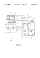
- FIG. 2 is a block diagram of a second level joint data and instruction TLB (JTLB) 103 in microprocessor 100.
- JTLB joint data and instruction
- FIG. 3 is a block diagram showing DTLB 101 of the present invention and address adder 306 used in a virtual memory address computation.
- FIG. 4 is a table showing the various conditions under which a "hit" occurs in DTLB 101, in accordance with the present invention.
- FIG. 1 shows an embodiment of the present invention in a first level data translation lookaside buffer (DTLB) 101 of a 64-bit microprocessor 100.
- DTLB first level data translation lookaside buffer
- microprocessor 100 has two levels of translation lookaside buffers (TLBs).
- TLB translation lookaside buffers
- the operations of microprocessor 100 are controlled by coprocessor unit 104 and system/memory control unit 105. Arithmetic and logical operations in microprocessor 100 are carried out in floating point unit 122 and integer unit 124.
- Microprocessor 100 includes an instruction cache and a data cache each organized as a 16K-byte two-way set associative cache.
- the instruction cache comprises an instruction portion 121 and instruction tag portions 151a and 151b.
- Instruction tags 151a and 151b are the two tag portions which are each compared to a physical memory address for set selection in the two-way set associative instruction cache.
- the data cache comprises a data portion 120 and data tag portions 150a and 150b. Both the data cache and the instruction cache are virtually indexed by a virtual memory address and physically tagged by a physical memory address provided on system address bus 152.
- Microprocessor 100 uses a 40-bit virtual memory address in three conventional operational modes: user, kernel and supervisor modes.
- the 40-bit virtual memory address is provided by a 64-bit addition of a 64-bit base address and a 16-bit offset.
- bits 40 to 60 in the result of the 64-bit addition are all zeroes.
- Virtual-to-physical memory address translation in microprocessor 100 is assisted by two levels of TLBs. In the first level, an instruction micro-TLB (ITLB) 102 and a data micro-TLB (DTLB) 101 are provided.
- the second level TLB is a joint TLB (JTLB) 103 for memory accesses to both data and instructions.
- Cache tag access in microprocessor 100 is performed simultaneously with virtual-to-physical address translation.
- the tags in the instruction and the data caches of microprocessor 100 are, however, physical addresses. This virtually indexed and physically tagged organization provides faster cache access and avoids extensive cache flushing during context switches. Such a cache organization also allows simultaneous cache access and virtual-to-physical memory address translation. Since both the instruction cache and the data cache of microprocessor 100 are two-way set associative caches, two sets of tags are compared in each cache to determine if a cache hit has occurred. Because the tags in each cache line are part of a physical memory address, set selection requires availability from the virtual-to-physical memory address translation the relevant bits of the physical address.
- JTLB 103 provides 96 page table entries in two RAM arrays, which are designated the even and the odd RAM arrays.
- FIG. 2 is a block diagram of JTLB 103.
- a virtual memory address is provided to address content addressable memory (CAM) units 201 and 202 in JTLB 103.
- CAM units 201 and 202 receive the translated bits of the virtual memory address.
- CAM unit 201 is a conventional content addressable memory for handling the portion of the virtual memory address which is always translated.
- CAM unit 202 is implemented using a modified larger CAM cell which allows the bits of the CAM cell to be selectably preset by a masking bit pattern to be "always matching" (i.e. masked) regardless of their values. If all the translated bits in the virtual memory address provided match a stored virtual memory address in the CAM units 201 and 202, match line 209 remains high to signal a TLB hit. Match line 209 activate a word line in each of RAM arrays 203 and 204. RAM arrays 203 and 204 output two sets of physical memory address bits.
- An edge detector 207 and multiplexers 205 together provide the masked bits of the virtual memory address as additional untranslated bits in place of the corresponding bits from RAM arrays 203 and 204.
- a priority circuit 206 and multiplexer 210 select between the two sets of physical memory address bits output from RAM arrays 203 and 204 to provide the translated physical address.
- JTLB 103 Because virtual-to-physical memory address translation through JTLB 103 is relatively more complex than a cache tag access, and because the virtual memory address must be completely computed (a 64 bit addition) before access to CAM units 201 and 202 can begin, the delay incurred in the virtual-to-physical memory address translation through JTLB 103 is considerably longer than the delay of a cache tag access. Since microprocessor 100 initiates a cache tag access simultaneously with virtual-to-physical address translation, and since a complete cache access requires the translated physical memory address to perform set selection, this delay through JTLB 103 is a limiting delay in the cache access.
- DTLB 101 is designed to provide a virtual-to-physical memory address translation which approximates the delay of the cache tag access, taking advantage that the result of the 64-bit addition yielding the virtual memory address can be predicted as soon as bit 15 of the result of the 64-bit addition is available. In this manner, virtual-to-physical memory address translation can begin before the virtual memory address computation is complete.
- FIG. 3 is a block diagram showing DTLB 101 and address adder 306, which is used in the 64-bit addition of a virtual memory address computation.
- latches 304 and 305 provide respectively to 64-bit adder 306 the bass address and the offset value used in computing a virtual memory address.
- adder 306 also provides the carry bit between bit 15 and bit 16 of the 64-bit sum.
- DTLB 101 comprises four identical entries for matching four virtual memory addresses to four physical addresses. Each entry comprises a virtual memory address matching circuit (i.e. one of circuits 301a-301d) and a corresponding physical address storage unit (i.e. one of circuits 302a-302d. Circuit 301a is shown in FIG. 3 in further detail. As shown in FIG. 3, circuit 301a comprises a storage unit 308, which stores the following components of a virtual memory address computation: (i) bits 16 to 63 of a base address, (ii) bits 12 to 15 of a virtual memory address output from adder 306, (iii) the carry bit 15 from the adder 306 and (iv) bit 15 of the offset. Storage unit 308 receives its input data from register 307, which is the input register for receiving input data into any of the four entries in DTLB 101.
- register 307 is the input register for receiving input data into any of the four entries in DTLB 101.
- Circuit 301a includes a comparator 309, which matches the current base address, bits 12 to 15 of the current sum, the current carry bit 15, and bit 15 of the current offset to the corresponding bits stored in storage unit 308.
- a DTLB hit occurs under any one of the six conditions shown in FIG. 4.
- the conditions tabulated in FIG. 4 provide all conditions under which the current sum in adder 306 would generate a virtual memory address matching the virtual memory address represented in storage unit 308 (i.e. a DTLB "hit").
- a DTLB hit results because, in adder 306, bits 16 to 63 of the base address are added to the sign extended bits of the offset value. Each of these sign extended bits has the same value of bit 15 (the "sign bit") of the offset value.
- bits 16 to 63 of the present and the previous base addresses are the same
- the sign bit of the present offset value is the same as the sign bit of the previous offset value
- carry bit 15 of the present sum is the same as the carry bit 15 of the previous sum (i.e. so that its affect on bits 16 to 63 in the resulting sum would be the same)
- bits 12 to 15 of the present sum are the same as bits 12 to 15 of the previous sum.
- Part (iv) of the four-part condition requires only bits 12 to 15 because bits 0 to 11 of a virtual memory address in this embodiment are not translated).
- Conditions 501 to 504 of FIG. 4 corresponds to instances in which the four-part condition is met.
- Condition 505 represents an instance in which the stored previous virtual memory address computation involves adding a base address to a positive offset value, and the current virtual memory address computation involves adding a negative offset value to a base address having the same bits 16 to 63 as corresponding bits of the previous base address and yielding the same resulting virtual memory address because of an "overflow" or "wrap-around" in the 64-bit sum.
- Condition 506 corresponds to the converse situation when the current offset value is positive, and the stored previous offset value is negative, both virtual memory address computations yielding the same virtual memory address.
- a DTLB hit can be determined as soon as bits 12 to 15 of the virtual memory address are computed.
- a DTLB hit occurs at any one of DTLB 101's virtual memory address memory circuit 301a-301d the content of the corresponding one of physical memory address storage units 302a-302d is selected by multiplexer 303 as the physical memory address, which is then provided for set selection at data cache 120.
- a more than one entry in DTLB 101 may map the same virtual memory address. For example, redundant mapping may occur when bits 16 to 63 of a stored base address and the corresponding bits of the current base address differ only at bit position 16, and a carry out or borrow occur in either the previous or the current computation. This condition, which may result in both the previous and current address computations yielding the same physical address, is not detected by the match conditions. Although redundant mappings do not cause a correctness problem in DTLB 101's operation, redundant mappings reduce the effective size of DTLB 101. In practice, however, this reduction in effective size is insignificant.
Landscapes
- Engineering & Computer Science (AREA)
- Theoretical Computer Science (AREA)
- Physics & Mathematics (AREA)
- General Engineering & Computer Science (AREA)
- General Physics & Mathematics (AREA)
- Memory System Of A Hierarchy Structure (AREA)
Abstract
Description
Claims (3)
Priority Applications (1)
| Application Number | Priority Date | Filing Date | Title |
|---|---|---|---|
| US08/732,862 US5953748A (en) | 1994-01-28 | 1996-10-15 | Processor with an efficient translation lookaside buffer which uses previous address computation results |
Applications Claiming Priority (2)
| Application Number | Priority Date | Filing Date | Title |
|---|---|---|---|
| US08/189,007 US5606683A (en) | 1994-01-28 | 1994-01-28 | Structure and method for virtual-to-physical address translation in a translation lookaside buffer |
| US08/732,862 US5953748A (en) | 1994-01-28 | 1996-10-15 | Processor with an efficient translation lookaside buffer which uses previous address computation results |
Related Parent Applications (1)
| Application Number | Title | Priority Date | Filing Date |
|---|---|---|---|
| US08/189,007 Division US5606683A (en) | 1994-01-28 | 1994-01-28 | Structure and method for virtual-to-physical address translation in a translation lookaside buffer |
Publications (1)
| Publication Number | Publication Date |
|---|---|
| US5953748A true US5953748A (en) | 1999-09-14 |
Family
ID=22695521
Family Applications (2)
| Application Number | Title | Priority Date | Filing Date |
|---|---|---|---|
| US08/189,007 Expired - Lifetime US5606683A (en) | 1994-01-28 | 1994-01-28 | Structure and method for virtual-to-physical address translation in a translation lookaside buffer |
| US08/732,862 Expired - Lifetime US5953748A (en) | 1994-01-28 | 1996-10-15 | Processor with an efficient translation lookaside buffer which uses previous address computation results |
Family Applications Before (1)
| Application Number | Title | Priority Date | Filing Date |
|---|---|---|---|
| US08/189,007 Expired - Lifetime US5606683A (en) | 1994-01-28 | 1994-01-28 | Structure and method for virtual-to-physical address translation in a translation lookaside buffer |
Country Status (1)
| Country | Link |
|---|---|
| US (2) | US5606683A (en) |
Cited By (12)
| Publication number | Priority date | Publication date | Assignee | Title |
|---|---|---|---|---|
| US6128697A (en) * | 1998-05-04 | 2000-10-03 | United Microelectronics Corp. | Selectively updateable mapped data storage system |
| US6374342B1 (en) * | 2000-01-31 | 2002-04-16 | Kabushiki Kaisha Toshiba | Translation lookaside buffer match detection using carry of lower side bit string of address addition |
| US6490658B1 (en) * | 1997-06-23 | 2002-12-03 | Sun Microsystems, Inc. | Data prefetch technique using prefetch cache, micro-TLB, and history file |
| US20030028749A1 (en) * | 2001-07-30 | 2003-02-06 | Hitachi, Ltd. | Data processor |
| US20040078545A1 (en) * | 2002-10-22 | 2004-04-22 | Min-Su Kim | High-speed translation lookaside buffer |
| US6772315B1 (en) | 2001-05-24 | 2004-08-03 | Rambus Inc | Translation lookaside buffer extended to provide physical and main-memory addresses |
| US20050021925A1 (en) * | 2003-07-25 | 2005-01-27 | Clark Lawrence T. | Accessing in parallel stored data for address translation |
| US20050050278A1 (en) * | 2003-09-03 | 2005-03-03 | Advanced Micro Devices, Inc. | Low power way-predicted cache |
| US20050050277A1 (en) * | 2003-09-03 | 2005-03-03 | Advanced Micro Devices, Inc. | MicroTLB and micro TAG for reducing power in a processor |
| US20090271590A1 (en) * | 2008-04-29 | 2009-10-29 | Jacob Carmona | Method and system for latency optimized ats usage |
| US20110145542A1 (en) * | 2009-12-15 | 2011-06-16 | Qualcomm Incorporated | Apparatuses, Systems, and Methods for Reducing Translation Lookaside Buffer (TLB) Lookups |
| CN107122128A (en) * | 2016-02-25 | 2017-09-01 | Arm 有限公司 | Data storage |
Families Citing this family (47)
| Publication number | Priority date | Publication date | Assignee | Title |
|---|---|---|---|---|
| US5937436A (en) * | 1996-07-01 | 1999-08-10 | Sun Microsystems, Inc | Network interface circuit including an address translation unit and flush control circuit and method for checking for invalid address translations |
| US5928352A (en) * | 1996-09-16 | 1999-07-27 | Intel Corporation | Method and apparatus for implementing a fully-associative translation look-aside buffer having a variable numbers of bits representing a virtual address entry |
| US6012131A (en) * | 1996-11-06 | 2000-01-04 | Hyundai Electronics Industries. Co., Ltd. | High speed translation lookaside buffer employing content address memory |
| US5781922A (en) * | 1996-11-19 | 1998-07-14 | International Business Machines Corporation | Page boundary caches |
| US6516386B1 (en) * | 1997-12-31 | 2003-02-04 | Intel Corporation | Method and apparatus for indexing a cache |
| US6134699A (en) * | 1998-01-30 | 2000-10-17 | International Business Machines Corporation | Method and apparatus for detecting virtual address parity error for a translation lookaside buffer |
| US7779236B1 (en) * | 1998-12-31 | 2010-08-17 | Stmicroelectronics, Inc. | Symbolic store-load bypass |
| US6412057B1 (en) | 1999-02-08 | 2002-06-25 | Kabushiki Kaisha Toshiba | Microprocessor with virtual-to-physical address translation using flags |
| GB2348980B (en) * | 1999-04-09 | 2004-05-12 | Pixelfusion Ltd | Parallel data processing systems |
| US20080184017A1 (en) * | 1999-04-09 | 2008-07-31 | Dave Stuttard | Parallel data processing apparatus |
| US7966475B2 (en) | 1999-04-09 | 2011-06-21 | Rambus Inc. | Parallel data processing apparatus |
| US20080007562A1 (en) * | 1999-04-09 | 2008-01-10 | Dave Stuttard | Parallel data processing apparatus |
| US7627736B2 (en) * | 1999-04-09 | 2009-12-01 | Clearspeed Technology Plc | Thread manager to control an array of processing elements |
| US20080016318A1 (en) * | 1999-04-09 | 2008-01-17 | Dave Stuttard | Parallel data processing apparatus |
| US8171263B2 (en) * | 1999-04-09 | 2012-05-01 | Rambus Inc. | Data processing apparatus comprising an array controller for separating an instruction stream processing instructions and data transfer instructions |
| US20080162874A1 (en) * | 1999-04-09 | 2008-07-03 | Dave Stuttard | Parallel data processing apparatus |
| JP5285828B2 (en) * | 1999-04-09 | 2013-09-11 | ラムバス・インコーポレーテッド | Parallel data processor |
| US20070294510A1 (en) * | 1999-04-09 | 2007-12-20 | Dave Stuttard | Parallel data processing apparatus |
| US8762691B2 (en) * | 1999-04-09 | 2014-06-24 | Rambus Inc. | Memory access consolidation for SIMD processing elements using transaction identifiers |
| US8169440B2 (en) * | 1999-04-09 | 2012-05-01 | Rambus Inc. | Parallel data processing apparatus |
| US20070242074A1 (en) * | 1999-04-09 | 2007-10-18 | Dave Stuttard | Parallel data processing apparatus |
| US8174530B2 (en) * | 1999-04-09 | 2012-05-08 | Rambus Inc. | Parallel date processing apparatus |
| US7506136B2 (en) * | 1999-04-09 | 2009-03-17 | Clearspeed Technology Plc | Parallel data processing apparatus |
| US20080008393A1 (en) * | 1999-04-09 | 2008-01-10 | Dave Stuttard | Parallel data processing apparatus |
| US7526630B2 (en) | 1999-04-09 | 2009-04-28 | Clearspeed Technology, Plc | Parallel data processing apparatus |
| US7802079B2 (en) * | 1999-04-09 | 2010-09-21 | Clearspeed Technology Limited | Parallel data processing apparatus |
| US6457068B1 (en) | 1999-08-30 | 2002-09-24 | Intel Corporation | Graphics address relocation table (GART) stored entirely in a local memory of an expansion bridge for address translation |
| TWI230897B (en) * | 2001-04-20 | 2005-04-11 | Ibm | Method for sharing a translation lookaside buffer between CPUs |
| US7206915B2 (en) * | 2004-06-03 | 2007-04-17 | Emc Corp | Virtual space manager for computer having a physical address extension feature |
| US7734901B2 (en) * | 2005-10-31 | 2010-06-08 | Mips Technologies, Inc. | Processor core and method for managing program counter redirection in an out-of-order processor pipeline |
| US7711934B2 (en) * | 2005-10-31 | 2010-05-04 | Mips Technologies, Inc. | Processor core and method for managing branch misprediction in an out-of-order processor pipeline |
| US20070204139A1 (en) | 2006-02-28 | 2007-08-30 | Mips Technologies, Inc. | Compact linked-list-based multi-threaded instruction graduation buffer |
| US7721071B2 (en) * | 2006-02-28 | 2010-05-18 | Mips Technologies, Inc. | System and method for propagating operand availability prediction bits with instructions through a pipeline in an out-of-order processor |
| US7370178B1 (en) * | 2006-07-14 | 2008-05-06 | Mips Technologies, Inc. | Method for latest producer tracking in an out-of-order processor, and applications thereof |
| US20080016326A1 (en) * | 2006-07-14 | 2008-01-17 | Mips Technologies, Inc. | Latest producer tracking in an out-of-order processor, and applications thereof |
| US7650465B2 (en) * | 2006-08-18 | 2010-01-19 | Mips Technologies, Inc. | Micro tag array having way selection bits for reducing data cache access power |
| US7657708B2 (en) * | 2006-08-18 | 2010-02-02 | Mips Technologies, Inc. | Methods for reducing data cache access power in a processor using way selection bits |
| US8032734B2 (en) * | 2006-09-06 | 2011-10-04 | Mips Technologies, Inc. | Coprocessor load data queue for interfacing an out-of-order execution unit with an in-order coprocessor |
| US7647475B2 (en) * | 2006-09-06 | 2010-01-12 | Mips Technologies, Inc. | System for synchronizing an in-order co-processor with an out-of-order processor using a co-processor interface store data queue |
| US7594079B2 (en) * | 2006-09-29 | 2009-09-22 | Mips Technologies, Inc. | Data cache virtual hint way prediction, and applications thereof |
| US8078846B2 (en) | 2006-09-29 | 2011-12-13 | Mips Technologies, Inc. | Conditional move instruction formed into one decoded instruction to be graduated and another decoded instruction to be invalidated |
| US9946547B2 (en) | 2006-09-29 | 2018-04-17 | Arm Finance Overseas Limited | Load/store unit for a processor, and applications thereof |
| US20080082793A1 (en) * | 2006-09-29 | 2008-04-03 | Mips Technologies, Inc. | Detection and prevention of write-after-write hazards, and applications thereof |
| US8438003B2 (en) * | 2007-04-12 | 2013-05-07 | Cadence Design Systems, Inc. | Methods for improved simulation of integrated circuit designs |
| US9009413B2 (en) * | 2012-12-21 | 2015-04-14 | Intel Corporation | Method and apparatus to implement lazy flush in a virtually tagged cache memory |
| US9652402B2 (en) * | 2014-12-23 | 2017-05-16 | Texas Instruments Incorporated | Hiding page translation miss latency in program memory controller by next page prefetch on crossing page boundary |
| US11113056B2 (en) * | 2019-11-27 | 2021-09-07 | Advanced Micro Devices, Inc. | Techniques for performing store-to-load forwarding |
Citations (7)
| Publication number | Priority date | Publication date | Assignee | Title |
|---|---|---|---|---|
| US4251860A (en) * | 1978-10-23 | 1981-02-17 | International Business Machines Corporation | Virtual addressing apparatus employing separate data paths for segment and offset portions of a virtual address and utilizing only the offset portion to calculate virtual address |
| US5150471A (en) * | 1989-04-20 | 1992-09-22 | Ncr Corporation | Method and apparatus for offset register address accessing |
| US5179674A (en) * | 1988-07-25 | 1993-01-12 | Digital Equipment Corporation | Method and apparatus for predicting valid performance of virtual-address to physical-address translations |
| US5263140A (en) * | 1991-01-23 | 1993-11-16 | Silicon Graphics, Inc. | Variable page size per entry translation look-aside buffer |
| US5335333A (en) * | 1991-10-29 | 1994-08-02 | Intel Corporation | Guess mechanism for faster address calculation in a pipelined microprocessor |
| US5381537A (en) * | 1991-12-06 | 1995-01-10 | International Business Machines Corporation | Large logical addressing method and means |
| US5420992A (en) * | 1991-03-11 | 1995-05-30 | Silicon Graphics, Inc. | Backward-compatible computer architecture with extended word size and address space |
-
1994
- 1994-01-28 US US08/189,007 patent/US5606683A/en not_active Expired - Lifetime
-
1996
- 1996-10-15 US US08/732,862 patent/US5953748A/en not_active Expired - Lifetime
Patent Citations (7)
| Publication number | Priority date | Publication date | Assignee | Title |
|---|---|---|---|---|
| US4251860A (en) * | 1978-10-23 | 1981-02-17 | International Business Machines Corporation | Virtual addressing apparatus employing separate data paths for segment and offset portions of a virtual address and utilizing only the offset portion to calculate virtual address |
| US5179674A (en) * | 1988-07-25 | 1993-01-12 | Digital Equipment Corporation | Method and apparatus for predicting valid performance of virtual-address to physical-address translations |
| US5150471A (en) * | 1989-04-20 | 1992-09-22 | Ncr Corporation | Method and apparatus for offset register address accessing |
| US5263140A (en) * | 1991-01-23 | 1993-11-16 | Silicon Graphics, Inc. | Variable page size per entry translation look-aside buffer |
| US5420992A (en) * | 1991-03-11 | 1995-05-30 | Silicon Graphics, Inc. | Backward-compatible computer architecture with extended word size and address space |
| US5335333A (en) * | 1991-10-29 | 1994-08-02 | Intel Corporation | Guess mechanism for faster address calculation in a pipelined microprocessor |
| US5381537A (en) * | 1991-12-06 | 1995-01-10 | International Business Machines Corporation | Large logical addressing method and means |
Cited By (22)
| Publication number | Priority date | Publication date | Assignee | Title |
|---|---|---|---|---|
| US6490658B1 (en) * | 1997-06-23 | 2002-12-03 | Sun Microsystems, Inc. | Data prefetch technique using prefetch cache, micro-TLB, and history file |
| US6128697A (en) * | 1998-05-04 | 2000-10-03 | United Microelectronics Corp. | Selectively updateable mapped data storage system |
| US6374342B1 (en) * | 2000-01-31 | 2002-04-16 | Kabushiki Kaisha Toshiba | Translation lookaside buffer match detection using carry of lower side bit string of address addition |
| US6772315B1 (en) | 2001-05-24 | 2004-08-03 | Rambus Inc | Translation lookaside buffer extended to provide physical and main-memory addresses |
| US6901501B2 (en) | 2001-07-30 | 2005-05-31 | Renesas Technology Corp. | Data processor |
| US20030028749A1 (en) * | 2001-07-30 | 2003-02-06 | Hitachi, Ltd. | Data processor |
| US6738890B2 (en) * | 2001-07-30 | 2004-05-18 | Renesas Technology Corp. | Data processor |
| US20040193778A1 (en) * | 2001-07-30 | 2004-09-30 | Renesas Technology Corp. | Data processor |
| US20040078545A1 (en) * | 2002-10-22 | 2004-04-22 | Min-Su Kim | High-speed translation lookaside buffer |
| US7035992B2 (en) * | 2002-10-22 | 2006-04-25 | Samsung Electronics Co., Ltd. | High-speed translation lookaside buffer |
| US20050021925A1 (en) * | 2003-07-25 | 2005-01-27 | Clark Lawrence T. | Accessing in parallel stored data for address translation |
| US20050050277A1 (en) * | 2003-09-03 | 2005-03-03 | Advanced Micro Devices, Inc. | MicroTLB and micro TAG for reducing power in a processor |
| US20050050278A1 (en) * | 2003-09-03 | 2005-03-03 | Advanced Micro Devices, Inc. | Low power way-predicted cache |
| US7117290B2 (en) * | 2003-09-03 | 2006-10-03 | Advanced Micro Devices, Inc. | MicroTLB and micro tag for reducing power in a processor |
| US20090271590A1 (en) * | 2008-04-29 | 2009-10-29 | Jacob Carmona | Method and system for latency optimized ats usage |
| US8850159B2 (en) * | 2008-04-29 | 2014-09-30 | Broadcom Corporation | Method and system for latency optimized ATS usage |
| US20110145542A1 (en) * | 2009-12-15 | 2011-06-16 | Qualcomm Incorporated | Apparatuses, Systems, and Methods for Reducing Translation Lookaside Buffer (TLB) Lookups |
| CN107122128A (en) * | 2016-02-25 | 2017-09-01 | Arm 有限公司 | Data storage |
| GB2547893A (en) * | 2016-02-25 | 2017-09-06 | Advanced Risc Mach Ltd | Data storage |
| GB2547893B (en) * | 2016-02-25 | 2018-06-06 | Advanced Risc Mach Ltd | Combining part of an offset with a corresponding part of a base address and comparing with a reference address |
| US10310735B2 (en) * | 2016-02-25 | 2019-06-04 | Arm Limited | Data storage |
| CN107122128B (en) * | 2016-02-25 | 2022-01-07 | Arm 有限公司 | Data storage |
Also Published As
| Publication number | Publication date |
|---|---|
| US5606683A (en) | 1997-02-25 |
Similar Documents
| Publication | Publication Date | Title |
|---|---|---|
| US5953748A (en) | Processor with an efficient translation lookaside buffer which uses previous address computation results | |
| KR920004400B1 (en) | Virtical computing system | |
| US6920531B2 (en) | Method and apparatus for updating and invalidating store data | |
| EP0701212B1 (en) | Data processor with set associative unit | |
| EP0734553B1 (en) | Split level cache | |
| EP0175091B1 (en) | Fast two-level dynamic address translation method and means | |
| JP2684196B2 (en) | Workstation | |
| US5353424A (en) | Fast tag compare and bank select in set associative cache | |
| US6138226A (en) | Logical cache memory storing logical and physical address information for resolving synonym problems | |
| US5761734A (en) | Token-based serialisation of instructions in a multiprocessor system | |
| US5586283A (en) | Method and apparatus for the reduction of tablewalk latencies in a translation look aside buffer | |
| US6266755B1 (en) | Translation lookaside buffer with virtual address conflict prevention | |
| US5604879A (en) | Single array address translator with segment and page invalidate ability and method of operation | |
| US6356990B1 (en) | Set-associative cache memory having a built-in set prediction array | |
| GB2293672A (en) | Virtual page memory buffer | |
| US5586296A (en) | Cache control system and method for selectively performing a non-cache access for instruction data depending on memory line access frequency | |
| US5682495A (en) | Fully associative address translation buffer having separate segment and page invalidation | |
| JP2001195303A (en) | Translation lookaside buffer whose function is parallelly distributed | |
| EP0676698A1 (en) | Address translation circuit | |
| US5940877A (en) | Cache address generation with and without carry-in | |
| US5535351A (en) | Address translator with by-pass circuit and method of operation | |
| US6044447A (en) | Method and apparatus for communicating translation command information in a multithreaded environment | |
| US6434670B1 (en) | Method and apparatus for efficiently managing caches with non-power-of-two congruence classes | |
| US5530822A (en) | Address translator and method of operation | |
| US8688952B2 (en) | Arithmetic processing unit and control method for evicting an entry from a TLB to another TLB |
Legal Events
| Date | Code | Title | Description |
|---|---|---|---|
| STCF | Information on status: patent grant |
Free format text: PATENTED CASE |
|
| FEPP | Fee payment procedure |
Free format text: PAYOR NUMBER ASSIGNED (ORIGINAL EVENT CODE: ASPN); ENTITY STATUS OF PATENT OWNER: LARGE ENTITY |
|
| REMI | Maintenance fee reminder mailed | ||
| FPAY | Fee payment |
Year of fee payment: 4 |
|
| SULP | Surcharge for late payment | ||
| FEPP | Fee payment procedure |
Free format text: PAYER NUMBER DE-ASSIGNED (ORIGINAL EVENT CODE: RMPN); ENTITY STATUS OF PATENT OWNER: LARGE ENTITY Free format text: PAYOR NUMBER ASSIGNED (ORIGINAL EVENT CODE: ASPN); ENTITY STATUS OF PATENT OWNER: LARGE ENTITY |
|
| FPAY | Fee payment |
Year of fee payment: 8 |
|
| FPAY | Fee payment |
Year of fee payment: 12 |
|
| AS | Assignment |
Owner name: PMC-SIERRA, INC., CALIFORNIA Free format text: MERGER;ASSIGNOR:QUANTUM EFFECT DEVICES, INC.;REEL/FRAME:037508/0717 Effective date: 20000711 |
|
| AS | Assignment |
Owner name: MORGAN STANLEY SENIOR FUNDING, INC., NEW YORK Free format text: PATENT SECURITY AGREEMENT;ASSIGNORS:MICROSEMI STORAGE SOLUTIONS, INC. (F/K/A PMC-SIERRA, INC.);MICROSEMI STORAGE SOLUTIONS (U.S.), INC. (F/K/A PMC-SIERRA US, INC.);REEL/FRAME:037689/0719 Effective date: 20160115 |
|
| AS | Assignment |
Owner name: MICROSEMI STORAGE SOLUTIONS, INC., CALIFORNIA Free format text: RELEASE BY SECURED PARTY;ASSIGNOR:MORGAN STANLEY SENIOR FUNDING, INC.;REEL/FRAME:046251/0271 Effective date: 20180529 Owner name: MICROSEMI STORAGE SOLUTIONS (U.S.), INC., CALIFORN Free format text: RELEASE BY SECURED PARTY;ASSIGNOR:MORGAN STANLEY SENIOR FUNDING, INC.;REEL/FRAME:046251/0271 Effective date: 20180529 |