US5959914A - Memory controller with error correction memory test application - Google Patents
Memory controller with error correction memory test application Download PDFInfo
- Publication number
- US5959914A US5959914A US09/049,316 US4931698A US5959914A US 5959914 A US5959914 A US 5959914A US 4931698 A US4931698 A US 4931698A US 5959914 A US5959914 A US 5959914A
- Authority
- US
- United States
- Prior art keywords
- test
- memory
- check bits
- data
- test data
- Prior art date
- Legal status (The legal status is an assumption and is not a legal conclusion. Google has not performed a legal analysis and makes no representation as to the accuracy of the status listed.)
- Expired - Lifetime
Links
Images


Classifications
-
- G—PHYSICS
- G06—COMPUTING; CALCULATING OR COUNTING
- G06F—ELECTRIC DIGITAL DATA PROCESSING
- G06F11/00—Error detection; Error correction; Monitoring
- G06F11/07—Responding to the occurrence of a fault, e.g. fault tolerance
- G06F11/08—Error detection or correction by redundancy in data representation, e.g. by using checking codes
- G06F11/10—Adding special bits or symbols to the coded information, e.g. parity check, casting out 9's or 11's
- G06F11/1008—Adding special bits or symbols to the coded information, e.g. parity check, casting out 9's or 11's in individual solid state devices
- G06F11/1048—Adding special bits or symbols to the coded information, e.g. parity check, casting out 9's or 11's in individual solid state devices using arrangements adapted for a specific error detection or correction feature
-
- G—PHYSICS
- G11—INFORMATION STORAGE
- G11C—STATIC STORES
- G11C29/00—Checking stores for correct operation ; Subsequent repair; Testing stores during standby or offline operation
- G11C29/04—Detection or location of defective memory elements, e.g. cell constructio details, timing of test signals
- G11C29/08—Functional testing, e.g. testing during refresh, power-on self testing [POST] or distributed testing
- G11C29/12—Built-in arrangements for testing, e.g. built-in self testing [BIST] or interconnection details
- G11C29/38—Response verification devices
- G11C29/42—Response verification devices using error correcting codes [ECC] or parity check
Definitions
- the present invention relates to testing of memory locations and, in particular, to testing memory locations containing test data and test check bits.
- ECC error correction and detection code
- ECC bits can be used to detect more than one bit (multiple bit) memory errors.
- common schemes for detecting multiple bit memory errors require the check bits to be stored in memory devices along with data bits, rather than storing all ECC or check bits in a separate device.
- This constraint related to where ECC bits can be stored relative to normal data bits must be taken into account when testing memory locations in which some of the memory locations store or contain normal data and the other of the memory locations store or contain ECC bits. Additional steps would be required to independently check such memory locations that include a combination of memory locations having normal data and also having ECC bits. That is, a first full test pattern sequence would be used to test a position or subset of the memory locations at a particular address and then a second full test pattern sequence would be used to test the remaining memory locations that were not tested during the first test pattern sequence.
- test data that usually is stored in memory locations for containing normal data is received by and stored in memory locations that are used to store check bits. Such test data written into memory locations intended for check bits is then read. After reading such test check bits from these memory locations intended to store ECC bits, the read data is checked to determine whether or not the check bit memory locations accurately stored and transmitted the expected check bits. If not, an indication is provided that these memory locations for storing ECC or check bits may have one or more faulty memory locations.
- testing of memory locations and memory devices in which a set of memory locations, which can be of any arrangement or configuration and that stores test data and test check bits, are tested using a single test pattern sequence to the memory devices.
- a single write operation, followed at some time later by a single read operation, can effectively test all of both test data bit locations and test check bit locations at the particular address(es). It is not required that the read of the word at the particular address(es) be tested immediately following a write to that location.
- the written test data and test check bits are subsequently read and checked to determine whether the read information (read test data and read test check bits) matches the written information. If not, then obtainable results of the test represent an error or lack of correspondence, which is indicative of one or more memory location faults.
- the apparatus of the present invention includes a memory controller defined as having a first or system side or interface and a second or memory side or interface. With respect to the system side, the memory controller functions to (1) provide an interface with a peripheral component interconnect (PCI) bus, although the control bus need not be a PCI bus but can be an internal bus via an embedded core processor or an external control bus such as the PCI bus; (2) provide RAID parity assist for queuing of exclusive or 5-operations; and (3) provide arbitration and control of a shared memory bus (SMB), although the present invention is not limited to such bus connections or operations.
- PCI peripheral component interconnect
- SMB shared memory bus
- the memory controller controls information transfers to/from the memory, in conjunction with its communication with the currently selected one of the PCI bus and the shared memory bus.
- information typically includes normal data and data or codes for detecting and correcting inaccuracies in the normal data.
- the transferred information includes test data and test check bits.
- the memory controller is involved in testing memory locations of the memory devices.
- a separate device which may include an IC (integrated circuit chip), is involved with inputting test data to the memory controller.
- Certain hardware or logic in the memory controller produces additional bits (additional test check and/or test data bits).
- the input, together with the subsequently produced, test data and test check bits are written to determined memory locations of the memory devices using the memory controller.
- input ports of the memory controller receive the previously stored test data and test check bits associated therewith.
- the memory controller includes hardware and logic for determining whether or not the test check bits that were read correspond to the test check bits that were written at some prior time. Preferably, this is accomplished by comparing predetermined bits of the test data with the test check bits that were read. More specifically, in producing the values, states or pattern of test check bits, such is based on values of at least some of the test data that accompanies the test check bits during the writing thereof to memory devices. Consequently, if a match or accurate comparison occurs between the test check bits and such data, it can be concluded that no memory location faults are present.
- test data that is simultaneously or substantially simultaneously read using the memory controller is also checked.
- this is accomplished by the memory controller transferring such test data to a desired module or device where a group comprising a number of bits, such as a byte or nibble, is compared with preceding or succeeding bytes or nibbles of the particular test data.
- the comparison is typically conducted using data stored or computed externally to the memory controller.
- the testing of one set of the memory locations containing the test data and the test check bits is conducted using one test pattern sequence for memory locations containing both test data and test check bits.
- the number of memory locations that are tested is a function of the capacity of the bus(es) (PCI, memory bus and SMB) connected to the memory controller ports.
- the test data includes 64 bits and the test check bits include 8 bits. Consequently, to test 72 bits of both test data and test check bits before another pass of testing, involving other memory locations having stored bits, the memory bus itself must be capable of handling the 72 bits, although the PCI and SMB interfaces need not be 72 bits.
- the PCI interface may handle 32 data bits and one parity bit, with the PCI module responsible for conversion between the two busses.
- test mode control signal or bit (test 13 chkbits) is utilized. That is, during test mode, the test control signal informs the memory controller that test data is being sent to it and the memory controller then functions in accordance with its test mode of operation.
- testing of memory locations storing both test data and test check bits is provided.
- the test check bits that are produced correspond to the values of at least some of the test data that the test check bits are associated with.
- the memory controller is also involved with controlling the transfer of normal data including error correction codes between memory devices and one or more control devices.
- the memory controller is configured to check for the accuracy of test check bits using corresponding values of test data while another device or module checks the accuracy of the test data that is associated with such test check bits.
- testing is conducted by writing, during a single write operation, a single test pattern sequence to memory locations being tested and then by reading of those same memory locations.
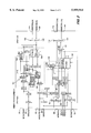
- FIG. 1 is a block diagram of the present invention including the memory controller
- FIG. 2 is a more detailed block diagram of the memory controller illustrating data paths for data transfers to/from the memory
- FIG. 3 is a table related to the transferring of normal data with ECC bits by the memory controller to desired storage locations
- FIG. 4 is a table related to the transferring of test data and test check bits to desired storage locations using the memory controller.
- FIG. 5 is a table presenting examples of mapping of information to be written using either the PCI bus or the SMB to the memory in normal and test modes.
- an apparatus 10 in which information is transferred relative to external memory 14 using a memory controller 18.
- the memory 14 is not limited to a particular configuration.
- the memory 14 can be stand-alone memory or embedded memory within the apparatus 10. When stand-alone memory, the memory may be in any configuration from where each bit is in a single stand alone device to where all the bits are in a single stand-alone device.
- memory 14 will be referred to as external memory 14; however, all memory configurations are contemplated for use with the present invention.
- the transferred information commonly includes data and accompanying bits associated with the data.
- the memory controller 18 is used in two modes of operation, a normal mode and a test mode.
- test data is generated for use in testing memory locations in the external memory 14.
- known values, states or patterns of data are generated, written to external memory 14 and then read back from the external memory 14.
- a determination is made as to whether or not the information read from the external memory 14 corresponds to the information that was written.
- a lack of correspondence is indicative of one or more memory location faults in the external memory 14.
- the test information includes the test data and the associated bits are test check bits.
- Test data and test check bits are intended to emulate or represent normal data and ECC bits.
- normal data and ECC bits are stored in the memory locations of the external memory 14. Values or states of the ECC bits are a function of the states of the normal data with which they are associated or derived. Although they need not be, the normal data and the ECC bits can be stored essentially simultaneously in the same memory devices.
- test check bits are provided and are mapped to memory locations that might receive or are intended to store the ECC bits. Consequently, testing of memory locations that contain or store important ECC bits useful in detecting and correcting inaccurate data is accomplished.
- the memory controller 18 With regard to the transfer of information using the memory controller 18, it includes a system side or interface 22 and a memory side or interface 26. Generally, the memory controller 18 has a number of functions. On the system side 22, the memory controller 18 serves as a buffered memory interface. As a memory interface, the memory controller 18 is a target for memory reads and writes using a peripheral component interconnect (PCI) bus 34, supporting up to two Gbytes of memory.
- PCI peripheral component interconnect
- the memory controller interface 22 in communication with the PCI bus 34, also supports access to internal registers through memory, I/O, or configuration read and write cycles.
- the system interface 22 of the memory controller 18 also communicates with a parity assist engine for RAID applications. The parity assist portion of the memory controller 18 operates independently of the PCI bus 34.
- the memory controller 18 fetches operands (data or RAID parity) from the external memory 14, calculates parity and writes the result back to the external memory 14.
- a shared memory bus (SMB) 40 also communicates with the system interface 22 of the memory controller 18.
- the SMB 40 allows for high-speed transfer between the external memory 14 and an external SMB device.
- this external SMB device has a number of primary functions including: providing a peripheral component interconnect to PCI bridge function between the PCI bus 34 and a secondary PCI bus; and supporting 64-bit addressing and 64-bit data transfer on this secondary PCI bus.
- the memory controller 18 transfers information to/from the external memory 14 using a memory bus 44 in functioning with the presently selected one of the PCI bus 34, the SMB 40 and the module involved with RAID applications.
- the PCI bus 34 and the SMB 40 can be utilized in testing of external memory bit locations, while the module involved with RAID applications would not be used in test mode.
- the memory controller 18 is responsible for utilizing such test information to conduct write and read operations directed to the external memory 14 in order to test a group or set of memory locations.
- the memory bus 44 is utilized in connection with the transfer of a selected one of normal or test information between the memory controller 18 and the external memory 14.
- the normal information includes data bits and ECC and the test information includes test data and test check bits.
- the external memory 14 comprises a number of memory devices 50a, 50b . . . 50n. Each of these memory devices 50 may constitute a single semiconductor memory having a number of memory locations for storing information including normal data and ECC bits associated therewith.
- the memory controller 18 is able to map, in a desired manner, which data and ECC bits are stored to particular memory locations of the external memory 14. Likewise, during the test mode of operation, the memory controller 18 is involved in mapping test data and test check bits to desired memory locations of each of the memory devices 50 in order to test such memory locations.
- the system side 22 of the memory controller 18 includes a number of ports. These ports include bi-directional data (DATA) and data parity (DATAP) ports 60, 64, respectively. These two ports 60, 64 communicate indirectly with the PCI bus 34 in transmitting information in both directions relative to the memory controller 18.
- the memory controller 18 also includes, in this embodiment, a number of uni-directional ports that are connected to bi-directional pads at the system interface 22.
- a shared memory input (MADIN) port 68 inputs data to the memory controller 18.
- a shared memory data parity (MADINP) port 72 receives parity data.
- shared data output (MADOUT) and shared memory data parity output (MADOUTP) ports 76, 80 output data and its associated parity (during the normal mode of operation) from the memory controller 18.
- the memory controller 18 includes a number of multiplexers, D flip-flops, inverters, as well as hardware useful in parity checking or parity generation useful during the normal mode of operation.
- the memory controller 18 receives a test mode control bit using the PCI bus 34.
- the PCI bus 34 communicates with a PCI slave module having control registers that store, among other items, the test mode control bit.
- the memory controller 18 includes a write ECC/test check bit multiplexer 84, which receives the test mode control bit as an input.
- the test mode control bit typically one or more test check bits, instead of ECC bits associated with normal data, are outputted by the multiplexer 84 and the remaining bits output therefrom are test data.
- the memory controller 18 further includes a write test check bit multiplexer 88.
- This multiplexer 88 receives two inputs from data source flip-flops 92, 96.
- the data source flip-flop 92 communicates with data input port 60 and data source flip-flop 96 communicates with shared memory data input port 68.
- the write test check bit multiplexer 88 receives data for use in testing from one of these two ports 60, 68.
- the multiplexer 88 outputs typically one or more test check bits and the remaining bits are test data.
- the values of the one or more test check bits that are output correspond to or are the same as some of the values of the test data.
- the output of the multiplexer 88 includes 8 bits, with the bits that are test check bits corresponding to the states or values of associated test data. That is, the associated test data from the selected source, either port 60 or port 68, is used to produce the bits output by the multiplexer 88.
- This same data for testing (includes usually both test data and test check bits) is received by a tri-state driver assembly 100.
- the driver assembly 100 includes tri-state drivers multiplexing data from five sources. Three of these sources are for read-modify-write cycles in normal data transfer operation that includes use of ECC bits, one of the five sources is for normal write data, and the other source is the test data.
- a write ECC/check bit output flip-flop 104 typically receives one or more test check bits, together with some test data, for outputting to the external memory 14 using an output ECC/test check bit (MEMECCOUT) port 108. Similarly, other of the test data and remaining test check bits are outputted therefrom and received by a write data output flip-flop 112.
- the output of this flip-flop 112 is transferred from the memory controller 18 using a memory data output (MEMDATOUT) port 116 for transfer to the external memory 14 using the memory bus 44.
- the memory bus 44 has a 64-bit capacity in which 64 bits of data are simultaneously transferred to the external memory 14.
- the memory controller 18 also includes an ECC check bit generation logic and parity check circuit or unit 120 that is utilized in the normal mode of operation.
- the output from this logic circuit 120 is also applied to the write ECC/test check bit multiplexer 84. In the absence of a test mode control bit, ECC bits are output by this multiplexer 84 to the write ECC/test check bit output flip-flop 104.
- the memory controller 18 also includes two memory input ports.
- a memory data input (MEMDATIN) port 124 communicates with the memory bus 44.
- a memory ECC input (MEMECCIN) port 128 also communicates with the memory bus 44.
- the memory ECC input port 128 typically receives at least some test check bits that were stored in the selected or desired memory locations of a particular memory device 50, while the memory data input port 124 receives the remaining test check bits.
- the memory controller 18 additionally includes a test mode data routing circuit or logic 132 which, in the test mode of operation, receives test data and test check bits from input flip-flops 136, 140.
- the test mode data routing circuit 132 is involved in reordering data received from the external memory 14, i.e., separating the test data and the test check or redundant bits. In that regard, the test mode data routing circuitry 132 prepares the input information for checking or comparison in connection with determining whether the test check bits that are received are accurate. As previously pointed out, it is necessary to verify that the information that was previously stored is received having the value or state, which is expected or intended.
- test mode compare logic or circuitry 150 is included in the memory controller 18. This compare logic or circuit 150 is involved in making the determination as to whether or not the obtained test check bits correspond to those values that were expected by making a comparison between the test check bits and certain of the test data bits. In one embodiment, the test check bits should correspond to certain of the test data. Such corresponding test data is input, together with the test check bits, into the test mode compare logic 150. Preferably, a single compare operation involving all of the test check bits is conducted. Based on this comparison, a determination can be made as to whether or not one or more of the test check bits is erroneous or inaccurate.
- test mode compare logic 150 outputs a signal indicating this failure and the address or addresses at which the test check bits were stored associated with this failure.
- the test data that was received with the test check bits is output by the memory controller 18 using one of the selected system output ports 60, 76.
- the test data output by such a selected port is sent to logic external to the memory controller 18 that is responsible for checking the accuracy of the test data by comparing portions, such as bytes, of the received data to determine whether or not it has been accurately received from the external memory 14. If not, a determination is made that the one or more memory locations associated with such erroneous data is faulty or subject to failure.
- the memory controller 18 also includes an ECC logic/parity generation circuit 158 that is utilized during normal data transfers for generating data parity and checking for proper ECC bits. During normal data transfer operation as well, one of the selected data parity ports 64, 80 is also utilized in the transfer of parity data from the memory controller 18.
- FIG. 3 illustrates 72 bits that are arranged in nibbles (4 bits).
- the normal data includes 64 bits and the ECC bits constitute the remaining 8 bits.
- the labeled DQ bits refer to bit positions in the memory bus 44.
- the letter "D” that is used on FIG. 3, together with the accompanying bit location, indicates that normal data is found at that particular bit location, while the letter "C" indicates that an ECC or check bit is found at that bit location.
- the locations of the "C" bits can be varied. What is important to note is that the mapped locations are known and they include locations for storing both data and ECC bits. In the example of FIG. 3, ECC bits are found in bit locations between data bit locations 25 and 26, 31 and 32, 57 and 58, and after data bit location 63. As can be further appreciated from this example, in order to test memory locations that store such normal data and ECC bits, for efficiency purposes, it is advantageous to simultaneously or substantially simultaneously test memory locations containing both data and code or check bits since they are intermingled as part of the 72 stored bits.
- FIG. 4 an illustrative example related to such simultaneous or substantially simultaneously testing is provided.
- 72 bits are arranged by nibbles (4 bits).
- the test check bits that are to be stored in connection with testing memory locations for containing ECC bits, for example, are produced from the test data.
- FIG. 4 illustrates that the bits located between test data bit locations 23 and 24 are identified as bit locations 00 through 07. This is intended to reflect the example in which the test check bits have values or states that correspond to the test data found in bit locations 00-07.
- test check bits of these memory locations can vary, and these eight bits could be located at any eight of the 72 bit locations.
- FIG. 5 further examples related to the mapping of data to the external memory 14 in normal and test modes, using either the PCI bus 34 or the SMB 40, are provided. As can be understood from this table, different external memory storage results are obtained, depending upon the particular data being written and the check bits.
- the operation of the present invention will be described in the context of the test mode by which desired memory locations in one or more of the memory devices 50a . . . 50n are tested.
- one write operation involving a single test pattern sequence is conducted and then a subsequent read operation is then conducted of the memory locations that were to store the test pattern sequence of this write operation.
- the memory controller 18 addresses 64 data bits (plus check bits) per unique address. This set of 64 data bits can be referred to as one quad word (QWord) Commonly, all accesses to the external memory 14 are QWord accesses.
- the memory controller 18 is configured to operate in test mode by the application of the test mode control bit (test-chkbits of FIG. 2) to the write ECC/test check bit multiplexer 84.
- Data for testing (test data and test check bits) is supplied to the memory controller 18 by a selected one of the bi-directional port 60 or the shared memory input port 68. From the selected one of the two ports 60, 68, the input data (e.g., 64 bits) is applied to the appropriate one of the two data source flip-flops 92, 96. The test data is outputted by whichever of the two flip-flops 92, 96 receives the data and transmits it to the test check bit multiplexer 88, which outputs additional bits including test check bits based on values or states of certain of the inputted data. In the disclosed embodiment, eight bits are output by the multiplexer 88.
- the input data e.g. 64 bits
- the test data is outputted by whichever of the two flip-flops 92, 96 receives the data and transmits it to the test check bit multiplexer 88, which outputs additional bits including test check bits based on values or states of certain of the inputted data. In the disclosed embodiment, eight bits are output by the multiple
- the test data and test check bits are also input to the tri-state driver assembly 100.
- the test data and test check bits constitute one of the sources of data that is input to the driver assembly 100.
- the memory address of the QWord is provided by conventional logic of the memory controller 18 that is not shown in FIG. 2. Further logic circuitry is also included in the memory controller 18 to provide various other memory control signals.
- the test data and test check bits output by the driver assembly 100 are applied to the write data output flip-flop 112. Under control of the test mode control bit input to the multiplexer 84, typically at least some test check bits are output therefrom to the write ECC/test check bit output flip-flop 104, while other test check bits are output from the flip-flop 112.
- test data and the test check bit data associated therewith are output from the memory controller 18 at ports 116, 108.
- the test data and test check bits are sent to the external memory 14 using the memory bus 44.
- the test data and test check bits are stored in memory locations of one or more of the memory devices 50a . . . 50n. This completes the particular one write operation of the test mode.
- test data and test check bits are accessed from those memory locations that were written to during the particular single pattern sequence write operation.
- the test data and the test check bits are received at the memory data input port 124 using the memory bus 44 and at the memory ECC input port 128 using the memory bus 44.
- the test data and test check bits are applied to the test mode data routing logic or circuit 132.
- test data and test check bits are outputted therefrom in a desired sequential arrangement in combination with the subsequent determination as to whether or not there is any fault or error in one or more of the test check bits.
- the test mode compare logic 150 compares values or states of certain test data with the values or states of the test check bits.
- the values of the test data associated with bit locations 00-07 are compared with the test check bits that are provided to the test mode compare logic 150 using the bus or conductors that carry the test check bits from the test mode data routing logic 132.
- an indication is outputted by the test mode compare logic 150.
- information related to such an error is maintained or stored in one or more registers accessible through the PCI interface.
- Such information can include the address or addresses in the external memory 14 to which such check bits were written or stored during the write operation of the test mode so that information is obtainable as to the identity of the memory locations that stored the test check bits which failed the comparison.
- test data itself is also tested by making comparisons, typically involving the test data and externally stored or computed data. In the illustrated embodiment, this comparison is conducted by logic separate from the memory controller 18. Upon completion of the comparisons and the attendant steps that are conducted when a lack of correspondence exists, the read operation of the test mode that is associated with the one test pattern sequence that was previously written is completed. Additional memory locations containing both test data and test check bits can be tested by appropriate mapping of test data and test check bits to these further memory locations so that the same steps are conducted and different ones of the memory devices 50a . . . 50n can be tested in the same manner.
Abstract
Description
Claims (18)
Priority Applications (1)
| Application Number | Priority Date | Filing Date | Title |
|---|---|---|---|
| US09/049,316 US5959914A (en) | 1998-03-27 | 1998-03-27 | Memory controller with error correction memory test application |
Applications Claiming Priority (1)
| Application Number | Priority Date | Filing Date | Title |
|---|---|---|---|
| US09/049,316 US5959914A (en) | 1998-03-27 | 1998-03-27 | Memory controller with error correction memory test application |
Publications (1)
| Publication Number | Publication Date |
|---|---|
| US5959914A true US5959914A (en) | 1999-09-28 |
Family
ID=21959177
Family Applications (1)
| Application Number | Title | Priority Date | Filing Date |
|---|---|---|---|
| US09/049,316 Expired - Lifetime US5959914A (en) | 1998-03-27 | 1998-03-27 | Memory controller with error correction memory test application |
Country Status (1)
| Country | Link |
|---|---|
| US (1) | US5959914A (en) |
Cited By (65)
| Publication number | Priority date | Publication date | Assignee | Title |
|---|---|---|---|---|
| US6163867A (en) * | 1998-08-28 | 2000-12-19 | Hewlett-Packard Company | Input-output pad testing using bi-directional pads |
| US20030190072A1 (en) * | 1998-08-28 | 2003-10-09 | Sean Adkins | Method and apparatus for processing images |
| US6643822B1 (en) * | 2000-05-23 | 2003-11-04 | Hewlett-Packard Development Company, L.P. | Computer system with greater than fifteen drive fault tolerance |
| US6647521B2 (en) * | 1998-07-01 | 2003-11-11 | Fujitsu Limited | Memory testing method and apparatus, and computer-readable recording medium |
| US6694479B1 (en) * | 2000-05-23 | 2004-02-17 | Hewlett-Packard Development Company, L.P. | Multiple drive failure recovery for a computer system having an array of storage drives |
| US20040054955A1 (en) * | 2002-09-12 | 2004-03-18 | Compaq Information Technologies Group, L.P. | Supporting cyclic redundancy checking for PCI-X |
| US20040120206A1 (en) * | 2002-12-18 | 2004-06-24 | Kang Hee Bok | Composite memory device |
| US6807649B1 (en) * | 2000-05-23 | 2004-10-19 | Hewlett-Packard Development Company, L.P. | Encryption keys for multiple drive fault tolerance |
| US20050036363A1 (en) * | 1996-05-24 | 2005-02-17 | Jeng-Jye Shau | High performance embedded semiconductor memory devices with multiple dimension first-level bit-lines |
| US20050044457A1 (en) * | 2003-08-19 | 2005-02-24 | Jeddeloh Joseph M. | System and method for on-board diagnostics of memory modules |
| US20050144403A1 (en) * | 2003-12-29 | 2005-06-30 | Jeddeloh Joseph M. | Memory hub and method for memory system performance monitoring |
| US20050164016A1 (en) * | 2004-01-27 | 2005-07-28 | Branagan Daniel J. | Metallic coatings on silicon substrates, and methods of forming metallic coatings on silicon substrates |
| US6988237B1 (en) | 2004-01-06 | 2006-01-17 | Marvell Semiconductor Israel Ltd. | Error-correction memory architecture for testing production errors |
| US20060036827A1 (en) * | 2004-07-30 | 2006-02-16 | International Business Machines Corporation | System, method and storage medium for providing segment level sparing |
| US7073099B1 (en) | 2002-05-30 | 2006-07-04 | Marvell International Ltd. | Method and apparatus for improving memory operation and yield |
| US20070005834A1 (en) * | 2005-06-30 | 2007-01-04 | Intel Corporation | Memory chips with buffer circuitry |
| US20070145363A1 (en) * | 2005-12-23 | 2007-06-28 | Fandrich Mickey L | Testing memory integrated circuits |
| US20070162826A1 (en) * | 2005-08-30 | 2007-07-12 | Major Karl L | Method for detecting error correction defects |
| US20070168829A1 (en) * | 1996-05-24 | 2007-07-19 | Jeng-Jye Shau | Methods to make DRAM fully compatible with SRAM |
| US7266635B1 (en) | 2004-07-22 | 2007-09-04 | Marvell Semiconductor Israel Ltd. | Address lookup apparatus having memory and content addressable memory |
| US20070234182A1 (en) * | 2006-03-31 | 2007-10-04 | Wickeraad John A | Error checking and correction (ECC) system and method |
| US20070277066A1 (en) * | 2006-05-23 | 2007-11-29 | Micron Technology, Inc. | System and method for more efficiently using error correction codes to facilitate memory device testing |
| US20070288707A1 (en) * | 2006-06-08 | 2007-12-13 | International Business Machines Corporation | Systems and methods for providing data modification operations in memory subsystems |
| US20070286078A1 (en) * | 2005-11-28 | 2007-12-13 | International Business Machines Corporation | Method and system for providing frame start indication in a memory system having indeterminate read data latency |
| US7310752B2 (en) | 2003-09-12 | 2007-12-18 | Micron Technology, Inc. | System and method for on-board timing margin testing of memory modules |
| US7310748B2 (en) | 2004-06-04 | 2007-12-18 | Micron Technology, Inc. | Memory hub tester interface and method for use thereof |
| US20080016280A1 (en) * | 2004-10-29 | 2008-01-17 | International Business Machines Corporation | System, method and storage medium for providing data caching and data compression in a memory subsystem |
| US20080040562A1 (en) * | 2006-08-09 | 2008-02-14 | International Business Machines Corporation | Systems and methods for providing distributed autonomous power management in a memory system |
| US20080040571A1 (en) * | 2004-10-29 | 2008-02-14 | International Business Machines Corporation | System, method and storage medium for bus calibration in a memory subsystem |
| US20080065938A1 (en) * | 2004-10-29 | 2008-03-13 | International Business Machines Corporation | System, method and storage medium for testing a memory module |
| US20080098277A1 (en) * | 2006-10-23 | 2008-04-24 | International Business Machines Corporation | High density high reliability memory module with power gating and a fault tolerant address and command bus |
| US20080104290A1 (en) * | 2004-10-29 | 2008-05-01 | International Business Machines Corporation | System, method and storage medium for providing a high speed test interface to a memory subsystem |
| US20080183977A1 (en) * | 2007-01-29 | 2008-07-31 | International Business Machines Corporation | Systems and methods for providing a dynamic memory bank page policy |
| US20080301509A1 (en) * | 2007-05-31 | 2008-12-04 | Kingtiger Technology (Canada) Inc. | Method and apparatus for testing integrated circuits by employing test vector patterns that satisfy passband requirements imposed by communication channels |
| WO2008155678A1 (en) * | 2007-06-20 | 2008-12-24 | Nxp B.V. | Detection of defective data sequences |
| US7478259B2 (en) | 2005-10-31 | 2009-01-13 | International Business Machines Corporation | System, method and storage medium for deriving clocks in a memory system |
| US7484161B2 (en) | 2004-10-29 | 2009-01-27 | International Business Machines Corporation | System, method and storage medium for providing fault detection and correction in a memory subsystem |
| US7490217B2 (en) | 2006-08-15 | 2009-02-10 | International Business Machines Corporation | Design structure for selecting memory busses according to physical memory organization information stored in virtual address translation tables |
| US20090115443A1 (en) * | 2007-11-01 | 2009-05-07 | Kingtiger Technology (Canada) Inc. | System and method for testing integrated circuit modules comprising a plurality of integrated circuit devices |
| US7539912B2 (en) | 2005-12-15 | 2009-05-26 | King Tiger Technology, Inc. | Method and apparatus for testing a fully buffered memory module |
| US7539842B2 (en) | 2006-08-15 | 2009-05-26 | International Business Machines Corporation | Computer memory system for selecting memory buses according to physical memory organization information stored in virtual address translation tables |
| US7539810B2 (en) | 2004-07-30 | 2009-05-26 | International Business Machines Corporation | System, method and storage medium for a multi-mode memory buffer device |
| US7587559B2 (en) | 2006-08-10 | 2009-09-08 | International Business Machines Corporation | Systems and methods for memory module power management |
| US7594055B2 (en) | 2006-05-24 | 2009-09-22 | International Business Machines Corporation | Systems and methods for providing distributed technology independent memory controllers |
| US7603526B2 (en) | 2007-01-29 | 2009-10-13 | International Business Machines Corporation | Systems and methods for providing dynamic memory pre-fetch |
| US7610423B2 (en) | 2004-10-29 | 2009-10-27 | International Business Machines Corporation | Service interface to a memory system |
| US20090306925A1 (en) * | 2008-06-09 | 2009-12-10 | Kingtiger Technology (Canada) Inc. | Systems and methods for testing integrated circuit devices |
| US7636813B2 (en) | 2006-05-22 | 2009-12-22 | International Business Machines Corporation | Systems and methods for providing remote pre-fetch buffers |
| US7640386B2 (en) | 2006-05-24 | 2009-12-29 | International Business Machines Corporation | Systems and methods for providing memory modules with multiple hub devices |
| US7669086B2 (en) | 2006-08-02 | 2010-02-23 | International Business Machines Corporation | Systems and methods for providing collision detection in a memory system |
| US7721140B2 (en) | 2007-01-02 | 2010-05-18 | International Business Machines Corporation | Systems and methods for improving serviceability of a memory system |
| US7765368B2 (en) | 2004-07-30 | 2010-07-27 | International Business Machines Corporation | System, method and storage medium for providing a serialized memory interface with a bus repeater |
| US7844771B2 (en) | 2004-10-29 | 2010-11-30 | International Business Machines Corporation | System, method and storage medium for a memory subsystem command interface |
| US20110179324A1 (en) * | 2010-01-19 | 2011-07-21 | Kingtiger Technology (Canada) Inc. | Testing apparatus and method for analyzing a memory module operating within an application system |
| US8296541B2 (en) | 2004-10-29 | 2012-10-23 | International Business Machines Corporation | Memory subsystem with positional read data latency |
| US8560907B1 (en) * | 2007-09-06 | 2013-10-15 | Altera Corporation | Debugging external interface |
| US8589643B2 (en) | 2003-10-20 | 2013-11-19 | Round Rock Research, Llc | Arbitration system and method for memory responses in a hub-based memory system |
| US8724408B2 (en) | 2011-11-29 | 2014-05-13 | Kingtiger Technology (Canada) Inc. | Systems and methods for testing and assembling memory modules |
| US8918686B2 (en) | 2010-08-18 | 2014-12-23 | Kingtiger Technology (Canada) Inc. | Determining data valid windows in a system and method for testing an integrated circuit device |
| US9003256B2 (en) | 2011-09-06 | 2015-04-07 | Kingtiger Technology (Canada) Inc. | System and method for testing integrated circuits by determining the solid timing window |
| US9117552B2 (en) | 2012-08-28 | 2015-08-25 | Kingtiger Technology(Canada), Inc. | Systems and methods for testing memory |
| US20160117217A1 (en) * | 2014-10-22 | 2016-04-28 | Xpliant, Inc. | Apparatus and a method of detecting errors on registers |
| US9825884B2 (en) | 2013-12-30 | 2017-11-21 | Cavium, Inc. | Protocol independent programmable switch (PIPS) software defined data center networks |
| CN108665939A (en) * | 2017-03-31 | 2018-10-16 | 厦门鑫忆讯科技有限公司 | The method and apparatus of ECC is provided for memory |
| US11928039B1 (en) * | 2022-11-01 | 2024-03-12 | Micron Technologies, Inc. | Data-transfer test mode |
Citations (9)
| Publication number | Priority date | Publication date | Assignee | Title |
|---|---|---|---|---|
| US4604750A (en) * | 1983-11-07 | 1986-08-05 | Digital Equipment Corporation | Pipeline error correction |
| US5006787A (en) * | 1989-06-12 | 1991-04-09 | Unisys Corporation | Self-testing circuitry for VLSI units |
| US5195099A (en) * | 1989-04-11 | 1993-03-16 | Mitsubishi Denki Kabushiki Kaisha | Semiconductor memory device having improved error correcting circuit |
| US5261068A (en) * | 1990-05-25 | 1993-11-09 | Dell Usa L.P. | Dual path memory retrieval system for an interleaved dynamic RAM memory unit |
| US5475693A (en) * | 1994-12-27 | 1995-12-12 | Intel Corporation | Error management processes for flash EEPROM memory arrays |
| US5541886A (en) * | 1994-12-27 | 1996-07-30 | Intel Corporation | Method and apparatus for storing control information in multi-bit non-volatile memory arrays |
| US5546402A (en) * | 1992-09-11 | 1996-08-13 | International Business Machines Corporation | Flash-erase-type nonvolatile semiconductor storage device |
| US5854795A (en) * | 1996-02-16 | 1998-12-29 | Kikusui Electronics Corporation | Memory capacity test method and computer system |
| US5872802A (en) * | 1996-05-03 | 1999-02-16 | Cypress Semiconductor Corp. | Parity generation and check circuit and method in read data path |
-
1998
- 1998-03-27 US US09/049,316 patent/US5959914A/en not_active Expired - Lifetime
Patent Citations (9)
| Publication number | Priority date | Publication date | Assignee | Title |
|---|---|---|---|---|
| US4604750A (en) * | 1983-11-07 | 1986-08-05 | Digital Equipment Corporation | Pipeline error correction |
| US5195099A (en) * | 1989-04-11 | 1993-03-16 | Mitsubishi Denki Kabushiki Kaisha | Semiconductor memory device having improved error correcting circuit |
| US5006787A (en) * | 1989-06-12 | 1991-04-09 | Unisys Corporation | Self-testing circuitry for VLSI units |
| US5261068A (en) * | 1990-05-25 | 1993-11-09 | Dell Usa L.P. | Dual path memory retrieval system for an interleaved dynamic RAM memory unit |
| US5546402A (en) * | 1992-09-11 | 1996-08-13 | International Business Machines Corporation | Flash-erase-type nonvolatile semiconductor storage device |
| US5475693A (en) * | 1994-12-27 | 1995-12-12 | Intel Corporation | Error management processes for flash EEPROM memory arrays |
| US5541886A (en) * | 1994-12-27 | 1996-07-30 | Intel Corporation | Method and apparatus for storing control information in multi-bit non-volatile memory arrays |
| US5854795A (en) * | 1996-02-16 | 1998-12-29 | Kikusui Electronics Corporation | Memory capacity test method and computer system |
| US5872802A (en) * | 1996-05-03 | 1999-02-16 | Cypress Semiconductor Corp. | Parity generation and check circuit and method in read data path |
Cited By (129)
| Publication number | Priority date | Publication date | Assignee | Title |
|---|---|---|---|---|
| US20070168829A1 (en) * | 1996-05-24 | 2007-07-19 | Jeng-Jye Shau | Methods to make DRAM fully compatible with SRAM |
| US20050036363A1 (en) * | 1996-05-24 | 2005-02-17 | Jeng-Jye Shau | High performance embedded semiconductor memory devices with multiple dimension first-level bit-lines |
| US6647521B2 (en) * | 1998-07-01 | 2003-11-11 | Fujitsu Limited | Memory testing method and apparatus, and computer-readable recording medium |
| US20030190072A1 (en) * | 1998-08-28 | 2003-10-09 | Sean Adkins | Method and apparatus for processing images |
| US6163867A (en) * | 1998-08-28 | 2000-12-19 | Hewlett-Packard Company | Input-output pad testing using bi-directional pads |
| US8015260B2 (en) | 2000-05-23 | 2011-09-06 | Hewlett-Packard Development Company, L.P. | Encryption keys for multiple drive fault tolerance |
| US6643822B1 (en) * | 2000-05-23 | 2003-11-04 | Hewlett-Packard Development Company, L.P. | Computer system with greater than fifteen drive fault tolerance |
| US6694479B1 (en) * | 2000-05-23 | 2004-02-17 | Hewlett-Packard Development Company, L.P. | Multiple drive failure recovery for a computer system having an array of storage drives |
| US6807649B1 (en) * | 2000-05-23 | 2004-10-19 | Hewlett-Packard Development Company, L.P. | Encryption keys for multiple drive fault tolerance |
| US20050028072A1 (en) * | 2000-05-23 | 2005-02-03 | Hewlett-Packard Development Company, L.P. | Encryption keys for multiple drive fault tolerance |
| US7962809B1 (en) | 2002-05-30 | 2011-06-14 | Marvell International Ltd. | Method and apparatus for improving memory operation and yield |
| US20070168781A1 (en) * | 2002-05-30 | 2007-07-19 | Sehat Sutardja | Fully-buffered dual in-line memory module with fault correction |
| US7818639B2 (en) | 2002-05-30 | 2010-10-19 | Marvell World Trade Ltd. | Fully-buffered dual in-line memory module with fault correction |
| US7818636B1 (en) | 2002-05-30 | 2010-10-19 | Marvell International Ltd. | Method and apparatus for improving memory operation and yield |
| US20110035545A1 (en) * | 2002-05-30 | 2011-02-10 | Sehat Sutardja | Fully-buffered dual in-line memory module with fault correction |
| US7814382B2 (en) | 2002-05-30 | 2010-10-12 | Marvell World Trade Ltd. | Fully-buffered dual in-line memory module with fault correction |
| US7073099B1 (en) | 2002-05-30 | 2006-07-04 | Marvell International Ltd. | Method and apparatus for improving memory operation and yield |
| US7809998B1 (en) | 2002-05-30 | 2010-10-05 | Marvell International Ltd. | Method and apparatus for improving memory operation and yield |
| US9158620B2 (en) | 2002-05-30 | 2015-10-13 | Marvell World Trade Ltd. | Systems and methods for testing pages of data stored in a memory module |
| US7823030B2 (en) | 2002-05-30 | 2010-10-26 | Marvell World Trade Ltd. | Fully-buffered dual in-line memory module with fault correction |
| US8745450B2 (en) | 2002-05-30 | 2014-06-03 | Marvell World Trade Ltd. | Fully-buffered dual in-line memory module with fault correction |
| US20110029752A1 (en) * | 2002-05-30 | 2011-02-03 | Sehat Sutardja | Fully-buffered dual in-line memory module with fault correction |
| US7870331B2 (en) | 2002-05-30 | 2011-01-11 | Marvell World Trade Ltd. | Fully-buffered dual in-line memory module with fault correction |
| US20070168812A1 (en) * | 2002-05-30 | 2007-07-19 | Sehat Sutardja | Fully-buffered dual in-line memory module with fault correction |
| US20070168810A1 (en) * | 2002-05-30 | 2007-07-19 | Sehat Sutardja | Fully-buffered dual in-line memory module with fault correction |
| US8281191B2 (en) | 2002-05-30 | 2012-10-02 | Marvell World Trade Ltd. | Fully-buffered dual in-line memory module with fault correction |
| US8103921B2 (en) | 2002-05-30 | 2012-01-24 | Marvell World Trade Ltd. | Fully-buffered dual in-line memory module with fault correction |
| US20040054955A1 (en) * | 2002-09-12 | 2004-03-18 | Compaq Information Technologies Group, L.P. | Supporting cyclic redundancy checking for PCI-X |
| US7447975B2 (en) * | 2002-09-12 | 2008-11-04 | Hewlett-Packard Development Company, L.P. | Supporting cyclic redundancy checking for PCI-X |
| US20040120206A1 (en) * | 2002-12-18 | 2004-06-24 | Kang Hee Bok | Composite memory device |
| US6990044B2 (en) * | 2002-12-18 | 2006-01-24 | Hynix Semiconductor Inc. | Composite memory device |
| US7913122B2 (en) | 2003-08-19 | 2011-03-22 | Round Rock Research, Llc | System and method for on-board diagnostics of memory modules |
| US7210059B2 (en) * | 2003-08-19 | 2007-04-24 | Micron Technology, Inc. | System and method for on-board diagnostics of memory modules |
| US7516363B2 (en) | 2003-08-19 | 2009-04-07 | Micron Technology, Inc. | System and method for on-board diagnostics of memory modules |
| US20050044457A1 (en) * | 2003-08-19 | 2005-02-24 | Jeddeloh Joseph M. | System and method for on-board diagnostics of memory modules |
| US7278060B2 (en) | 2003-08-19 | 2007-10-02 | Micron Technology, Inc. | System and method for on-board diagnostics of memory modules |
| US7958412B2 (en) | 2003-09-12 | 2011-06-07 | Round Rock Research, Llc | System and method for on-board timing margin testing of memory modules |
| US7689879B2 (en) | 2003-09-12 | 2010-03-30 | Micron Technology, Inc. | System and method for on-board timing margin testing of memory modules |
| US20100153794A1 (en) * | 2003-09-12 | 2010-06-17 | Round Rock Research, Llc | System and method for on-board timing margin testing of memory modules |
| US7310752B2 (en) | 2003-09-12 | 2007-12-18 | Micron Technology, Inc. | System and method for on-board timing margin testing of memory modules |
| US8589643B2 (en) | 2003-10-20 | 2013-11-19 | Round Rock Research, Llc | Arbitration system and method for memory responses in a hub-based memory system |
| US7216196B2 (en) | 2003-12-29 | 2007-05-08 | Micron Technology, Inc. | Memory hub and method for memory system performance monitoring |
| US7360011B2 (en) | 2003-12-29 | 2008-04-15 | Micron Technology, Inc. | Memory hub and method for memory system performance monitoring |
| US20050144403A1 (en) * | 2003-12-29 | 2005-06-30 | Jeddeloh Joseph M. | Memory hub and method for memory system performance monitoring |
| US20080140904A1 (en) * | 2003-12-29 | 2008-06-12 | Micron Technology, Inc. | Memory hub and method for memory system performance monitoring |
| US7533213B2 (en) | 2003-12-29 | 2009-05-12 | Micron Technology, Inc. | Memory hub and method for memory system performance monitoring |
| US20070174562A1 (en) * | 2003-12-29 | 2007-07-26 | Micron Technology, Inc. | Memory hub and method for memory system performance monitoring |
| US7984358B1 (en) | 2004-01-06 | 2011-07-19 | Marvell Israel (M.I.S.L) Ltd. | Error-correction memory architecture for testing production errors |
| US7206988B1 (en) | 2004-01-06 | 2007-04-17 | Marvell Semiconductor Israel Ltd. | Error-correction memory architecture for testing production errors |
| US7478308B1 (en) | 2004-01-06 | 2009-01-13 | Marvell Israel (M.I.S.L.) Ltd. | Error-correction memory architecture for testing production |
| US6988237B1 (en) | 2004-01-06 | 2006-01-17 | Marvell Semiconductor Israel Ltd. | Error-correction memory architecture for testing production errors |
| US20050164016A1 (en) * | 2004-01-27 | 2005-07-28 | Branagan Daniel J. | Metallic coatings on silicon substrates, and methods of forming metallic coatings on silicon substrates |
| US7310748B2 (en) | 2004-06-04 | 2007-12-18 | Micron Technology, Inc. | Memory hub tester interface and method for use thereof |
| US7823024B2 (en) | 2004-06-04 | 2010-10-26 | Micron Technology, Inc. | Memory hub tester interface and method for use thereof |
| US7266635B1 (en) | 2004-07-22 | 2007-09-04 | Marvell Semiconductor Israel Ltd. | Address lookup apparatus having memory and content addressable memory |
| US7765368B2 (en) | 2004-07-30 | 2010-07-27 | International Business Machines Corporation | System, method and storage medium for providing a serialized memory interface with a bus repeater |
| US7539810B2 (en) | 2004-07-30 | 2009-05-26 | International Business Machines Corporation | System, method and storage medium for a multi-mode memory buffer device |
| US20060036827A1 (en) * | 2004-07-30 | 2006-02-16 | International Business Machines Corporation | System, method and storage medium for providing segment level sparing |
| US7539800B2 (en) * | 2004-07-30 | 2009-05-26 | International Business Machines Corporation | System, method and storage medium for providing segment level sparing |
| US8140942B2 (en) | 2004-10-29 | 2012-03-20 | International Business Machines Corporation | System, method and storage medium for providing fault detection and correction in a memory subsystem |
| US20080016280A1 (en) * | 2004-10-29 | 2008-01-17 | International Business Machines Corporation | System, method and storage medium for providing data caching and data compression in a memory subsystem |
| US7475316B2 (en) | 2004-10-29 | 2009-01-06 | International Business Machines Corporation | System, method and storage medium for providing a high speed test interface to a memory subsystem |
| US7480759B2 (en) | 2004-10-29 | 2009-01-20 | International Business Machines Corporation | System, method and storage medium for providing data caching and data compression in a memory subsystem |
| US7484161B2 (en) | 2004-10-29 | 2009-01-27 | International Business Machines Corporation | System, method and storage medium for providing fault detection and correction in a memory subsystem |
| US20080104290A1 (en) * | 2004-10-29 | 2008-05-01 | International Business Machines Corporation | System, method and storage medium for providing a high speed test interface to a memory subsystem |
| US20080065938A1 (en) * | 2004-10-29 | 2008-03-13 | International Business Machines Corporation | System, method and storage medium for testing a memory module |
| US7590882B2 (en) | 2004-10-29 | 2009-09-15 | International Business Machines Corporation | System, method and storage medium for bus calibration in a memory subsystem |
| US20080040571A1 (en) * | 2004-10-29 | 2008-02-14 | International Business Machines Corporation | System, method and storage medium for bus calibration in a memory subsystem |
| US7844771B2 (en) | 2004-10-29 | 2010-11-30 | International Business Machines Corporation | System, method and storage medium for a memory subsystem command interface |
| US7480830B2 (en) | 2004-10-29 | 2009-01-20 | International Business Machines Corporation | System, method and storage medium for testing a memory module |
| US7610423B2 (en) | 2004-10-29 | 2009-10-27 | International Business Machines Corporation | Service interface to a memory system |
| US8296541B2 (en) | 2004-10-29 | 2012-10-23 | International Business Machines Corporation | Memory subsystem with positional read data latency |
| US20070005834A1 (en) * | 2005-06-30 | 2007-01-04 | Intel Corporation | Memory chips with buffer circuitry |
| US20070162826A1 (en) * | 2005-08-30 | 2007-07-12 | Major Karl L | Method for detecting error correction defects |
| US7934115B2 (en) | 2005-10-31 | 2011-04-26 | International Business Machines Corporation | Deriving clocks in a memory system |
| US7478259B2 (en) | 2005-10-31 | 2009-01-13 | International Business Machines Corporation | System, method and storage medium for deriving clocks in a memory system |
| US8495328B2 (en) | 2005-11-28 | 2013-07-23 | International Business Machines Corporation | Providing frame start indication in a memory system having indeterminate read data latency |
| US7685392B2 (en) | 2005-11-28 | 2010-03-23 | International Business Machines Corporation | Providing indeterminate read data latency in a memory system |
| US20070286078A1 (en) * | 2005-11-28 | 2007-12-13 | International Business Machines Corporation | Method and system for providing frame start indication in a memory system having indeterminate read data latency |
| US8145868B2 (en) | 2005-11-28 | 2012-03-27 | International Business Machines Corporation | Method and system for providing frame start indication in a memory system having indeterminate read data latency |
| US8151042B2 (en) | 2005-11-28 | 2012-04-03 | International Business Machines Corporation | Method and system for providing identification tags in a memory system having indeterminate data response times |
| US8327105B2 (en) | 2005-11-28 | 2012-12-04 | International Business Machines Corporation | Providing frame start indication in a memory system having indeterminate read data latency |
| US7539912B2 (en) | 2005-12-15 | 2009-05-26 | King Tiger Technology, Inc. | Method and apparatus for testing a fully buffered memory module |
| US20070145363A1 (en) * | 2005-12-23 | 2007-06-28 | Fandrich Mickey L | Testing memory integrated circuits |
| US7624316B2 (en) * | 2005-12-23 | 2009-11-24 | Intel Corporation | Apparatus and method for testing removable flash memory devices |
| US20070234182A1 (en) * | 2006-03-31 | 2007-10-04 | Wickeraad John A | Error checking and correction (ECC) system and method |
| US8245109B2 (en) * | 2006-03-31 | 2012-08-14 | Hewlett-Packard Development Company, L.P. | Error checking and correction (ECC) system and method |
| US7636813B2 (en) | 2006-05-22 | 2009-12-22 | International Business Machines Corporation | Systems and methods for providing remote pre-fetch buffers |
| US20070277066A1 (en) * | 2006-05-23 | 2007-11-29 | Micron Technology, Inc. | System and method for more efficiently using error correction codes to facilitate memory device testing |
| US7506226B2 (en) | 2006-05-23 | 2009-03-17 | Micron Technology, Inc. | System and method for more efficiently using error correction codes to facilitate memory device testing |
| US7594055B2 (en) | 2006-05-24 | 2009-09-22 | International Business Machines Corporation | Systems and methods for providing distributed technology independent memory controllers |
| US7640386B2 (en) | 2006-05-24 | 2009-12-29 | International Business Machines Corporation | Systems and methods for providing memory modules with multiple hub devices |
| US20070288707A1 (en) * | 2006-06-08 | 2007-12-13 | International Business Machines Corporation | Systems and methods for providing data modification operations in memory subsystems |
| US7584336B2 (en) | 2006-06-08 | 2009-09-01 | International Business Machines Corporation | Systems and methods for providing data modification operations in memory subsystems |
| US7669086B2 (en) | 2006-08-02 | 2010-02-23 | International Business Machines Corporation | Systems and methods for providing collision detection in a memory system |
| US7581073B2 (en) | 2006-08-09 | 2009-08-25 | International Business Machines Corporation | Systems and methods for providing distributed autonomous power management in a memory system |
| US20080040562A1 (en) * | 2006-08-09 | 2008-02-14 | International Business Machines Corporation | Systems and methods for providing distributed autonomous power management in a memory system |
| US7587559B2 (en) | 2006-08-10 | 2009-09-08 | International Business Machines Corporation | Systems and methods for memory module power management |
| US7539842B2 (en) | 2006-08-15 | 2009-05-26 | International Business Machines Corporation | Computer memory system for selecting memory buses according to physical memory organization information stored in virtual address translation tables |
| US7636833B2 (en) | 2006-08-15 | 2009-12-22 | International Business Machines Corporation | Method for selecting memory busses according to physical memory organization information associated with virtual address translation tables |
| US7490217B2 (en) | 2006-08-15 | 2009-02-10 | International Business Machines Corporation | Design structure for selecting memory busses according to physical memory organization information stored in virtual address translation tables |
| US20080098277A1 (en) * | 2006-10-23 | 2008-04-24 | International Business Machines Corporation | High density high reliability memory module with power gating and a fault tolerant address and command bus |
| US7870459B2 (en) | 2006-10-23 | 2011-01-11 | International Business Machines Corporation | High density high reliability memory module with power gating and a fault tolerant address and command bus |
| US7721140B2 (en) | 2007-01-02 | 2010-05-18 | International Business Machines Corporation | Systems and methods for improving serviceability of a memory system |
| US7603526B2 (en) | 2007-01-29 | 2009-10-13 | International Business Machines Corporation | Systems and methods for providing dynamic memory pre-fetch |
| US7606988B2 (en) | 2007-01-29 | 2009-10-20 | International Business Machines Corporation | Systems and methods for providing a dynamic memory bank page policy |
| US20080183977A1 (en) * | 2007-01-29 | 2008-07-31 | International Business Machines Corporation | Systems and methods for providing a dynamic memory bank page policy |
| US20080301509A1 (en) * | 2007-05-31 | 2008-12-04 | Kingtiger Technology (Canada) Inc. | Method and apparatus for testing integrated circuits by employing test vector patterns that satisfy passband requirements imposed by communication channels |
| US7620861B2 (en) | 2007-05-31 | 2009-11-17 | Kingtiger Technology (Canada) Inc. | Method and apparatus for testing integrated circuits by employing test vector patterns that satisfy passband requirements imposed by communication channels |
| WO2008155678A1 (en) * | 2007-06-20 | 2008-12-24 | Nxp B.V. | Detection of defective data sequences |
| US8560907B1 (en) * | 2007-09-06 | 2013-10-15 | Altera Corporation | Debugging external interface |
| US7757144B2 (en) | 2007-11-01 | 2010-07-13 | Kingtiger Technology (Canada) Inc. | System and method for testing integrated circuit modules comprising a plurality of integrated circuit devices |
| US20090115443A1 (en) * | 2007-11-01 | 2009-05-07 | Kingtiger Technology (Canada) Inc. | System and method for testing integrated circuit modules comprising a plurality of integrated circuit devices |
| US7848899B2 (en) | 2008-06-09 | 2010-12-07 | Kingtiger Technology (Canada) Inc. | Systems and methods for testing integrated circuit devices |
| US20090306925A1 (en) * | 2008-06-09 | 2009-12-10 | Kingtiger Technology (Canada) Inc. | Systems and methods for testing integrated circuit devices |
| US8356215B2 (en) | 2010-01-19 | 2013-01-15 | Kingtiger Technology (Canada) Inc. | Testing apparatus and method for analyzing a memory module operating within an application system |
| US20110179324A1 (en) * | 2010-01-19 | 2011-07-21 | Kingtiger Technology (Canada) Inc. | Testing apparatus and method for analyzing a memory module operating within an application system |
| US8918686B2 (en) | 2010-08-18 | 2014-12-23 | Kingtiger Technology (Canada) Inc. | Determining data valid windows in a system and method for testing an integrated circuit device |
| US9003256B2 (en) | 2011-09-06 | 2015-04-07 | Kingtiger Technology (Canada) Inc. | System and method for testing integrated circuits by determining the solid timing window |
| US8724408B2 (en) | 2011-11-29 | 2014-05-13 | Kingtiger Technology (Canada) Inc. | Systems and methods for testing and assembling memory modules |
| US9224500B2 (en) | 2011-11-29 | 2015-12-29 | Kingtiger Technology (Canada) Inc. | Systems and methods for testing and assembling memory modules |
| US9117552B2 (en) | 2012-08-28 | 2015-08-25 | Kingtiger Technology(Canada), Inc. | Systems and methods for testing memory |
| US9825884B2 (en) | 2013-12-30 | 2017-11-21 | Cavium, Inc. | Protocol independent programmable switch (PIPS) software defined data center networks |
| US10785169B2 (en) | 2013-12-30 | 2020-09-22 | Marvell Asia Pte, Ltd. | Protocol independent programmable switch (PIPS) for software defined data center networks |
| US11824796B2 (en) | 2013-12-30 | 2023-11-21 | Marvell Asia Pte, Ltd. | Protocol independent programmable switch (PIPS) for software defined data center networks |
| US20160117217A1 (en) * | 2014-10-22 | 2016-04-28 | Xpliant, Inc. | Apparatus and a method of detecting errors on registers |
| US10656992B2 (en) * | 2014-10-22 | 2020-05-19 | Cavium International | Apparatus and a method of detecting errors on registers |
| CN108665939A (en) * | 2017-03-31 | 2018-10-16 | 厦门鑫忆讯科技有限公司 | The method and apparatus of ECC is provided for memory |
| US11928039B1 (en) * | 2022-11-01 | 2024-03-12 | Micron Technologies, Inc. | Data-transfer test mode |
Similar Documents
| Publication | Publication Date | Title |
|---|---|---|
| US5959914A (en) | Memory controller with error correction memory test application | |
| US4541094A (en) | Self-checking computer circuitry | |
| US5033048A (en) | Memory selftest method and apparatus same | |
| US8081529B2 (en) | Circuit and method for testing multi-device systems | |
| EP0319188B1 (en) | Method and apparatus for data integrity checking with fault tolerance | |
| US8074159B2 (en) | Method and apparatus for detecting communication errors on a bus | |
| US4926426A (en) | Error correction check during write cycles | |
| US20040165446A1 (en) | Obtaining data mask mapping information | |
| US4809276A (en) | Memory failure detection apparatus | |
| EP0831496B1 (en) | A method and system for testing memory | |
| US6957307B2 (en) | Mapping data masks in hardware by controller programming | |
| EP0505914B1 (en) | Programmable read only memory device having a test tool for testing the error checking and correction circuit | |
| KR940001146B1 (en) | System for checking comparision check function of information processing apparatus | |
| US5436856A (en) | Self testing computer system with circuits including test registers | |
| US4761783A (en) | Apparatus and method for reporting occurrences of errors in signals stored in a data processor | |
| JP3570388B2 (en) | Memory diagnostic device and diagnostic method | |
| US5357529A (en) | Error detecting and correcting apparatus and method with transparent test mode | |
| EP0366757B1 (en) | Memory selftest method and apparatus | |
| JPH0442691B2 (en) | ||
| JPH045213B2 (en) | ||
| TW200915330A (en) | Method for performing memory diagnostics using a programmable diagnostic memory module | |
| JPS63753A (en) | Test system for memory error checking and correcting circuit | |
| JPS6035695B2 (en) | Memory test method | |
| JPH0346047A (en) | Inspection circuit | |
| JPS63280342A (en) | Shift path trouble diagnosing system |
Legal Events
| Date | Code | Title | Description |
|---|---|---|---|
| AS | Assignment |
Owner name: SYMBIOS, INC., COLORADO Free format text: ASSIGNMENT OF ASSIGNORS INTEREST;ASSIGNORS:GATES, DENNIS F.;GREENFIELD, SCOTT E.;LANGFORD, II, THOMAS L.;REEL/FRAME:009126/0209 Effective date: 19980326 |
|
| AS | Assignment |
Owner name: LSI LOGIC CORPORATION, CALIFORNIA Free format text: ASSIGNMENT OF ASSIGNORS INTEREST;ASSIGNOR:SYMBIOS, INC.;REEL/FRAME:009500/0554 Effective date: 19980922 |
|
| STCF | Information on status: patent grant |
Free format text: PATENTED CASE |
|
| FPAY | Fee payment |
Year of fee payment: 4 |
|
| FPAY | Fee payment |
Year of fee payment: 8 |
|
| FEPP | Fee payment procedure |
Free format text: PAYOR NUMBER ASSIGNED (ORIGINAL EVENT CODE: ASPN); ENTITY STATUS OF PATENT OWNER: LARGE ENTITY Free format text: PAYER NUMBER DE-ASSIGNED (ORIGINAL EVENT CODE: RMPN); ENTITY STATUS OF PATENT OWNER: LARGE ENTITY |
|
| FPAY | Fee payment |
Year of fee payment: 12 |
|
| AS | Assignment |
Owner name: DEUTSCHE BANK AG NEW YORK BRANCH, AS COLLATERAL AG Free format text: PATENT SECURITY AGREEMENT;ASSIGNORS:LSI CORPORATION;AGERE SYSTEMS LLC;REEL/FRAME:032856/0031 Effective date: 20140506 |
|
| AS | Assignment |
Owner name: LSI CORPORATION, CALIFORNIA Free format text: CHANGE OF NAME;ASSIGNOR:LSI LOGIC CORPORATION;REEL/FRAME:033102/0270 Effective date: 20070406 |
|
| AS | Assignment |
Owner name: AVAGO TECHNOLOGIES GENERAL IP (SINGAPORE) PTE. LTD Free format text: ASSIGNMENT OF ASSIGNORS INTEREST;ASSIGNOR:LSI CORPORATION;REEL/FRAME:035390/0388 Effective date: 20140814 |
|
| AS | Assignment |
Owner name: LSI CORPORATION, CALIFORNIA Free format text: TERMINATION AND RELEASE OF SECURITY INTEREST IN PATENT RIGHTS (RELEASES RF 032856-0031);ASSIGNOR:DEUTSCHE BANK AG NEW YORK BRANCH, AS COLLATERAL AGENT;REEL/FRAME:037684/0039 Effective date: 20160201 Owner name: AGERE SYSTEMS LLC, PENNSYLVANIA Free format text: TERMINATION AND RELEASE OF SECURITY INTEREST IN PATENT RIGHTS (RELEASES RF 032856-0031);ASSIGNOR:DEUTSCHE BANK AG NEW YORK BRANCH, AS COLLATERAL AGENT;REEL/FRAME:037684/0039 Effective date: 20160201 |
|
| AS | Assignment |
Owner name: BANK OF AMERICA, N.A., AS COLLATERAL AGENT, NORTH CAROLINA Free format text: PATENT SECURITY AGREEMENT;ASSIGNOR:AVAGO TECHNOLOGIES GENERAL IP (SINGAPORE) PTE. LTD.;REEL/FRAME:037808/0001 Effective date: 20160201 Owner name: BANK OF AMERICA, N.A., AS COLLATERAL AGENT, NORTH Free format text: PATENT SECURITY AGREEMENT;ASSIGNOR:AVAGO TECHNOLOGIES GENERAL IP (SINGAPORE) PTE. LTD.;REEL/FRAME:037808/0001 Effective date: 20160201 |
|
| AS | Assignment |
Owner name: AVAGO TECHNOLOGIES GENERAL IP (SINGAPORE) PTE. LTD., SINGAPORE Free format text: TERMINATION AND RELEASE OF SECURITY INTEREST IN PATENTS;ASSIGNOR:BANK OF AMERICA, N.A., AS COLLATERAL AGENT;REEL/FRAME:041710/0001 Effective date: 20170119 Owner name: AVAGO TECHNOLOGIES GENERAL IP (SINGAPORE) PTE. LTD Free format text: TERMINATION AND RELEASE OF SECURITY INTEREST IN PATENTS;ASSIGNOR:BANK OF AMERICA, N.A., AS COLLATERAL AGENT;REEL/FRAME:041710/0001 Effective date: 20170119 |
|
| AS | Assignment |
Owner name: AVAGO TECHNOLOGIES INTERNATIONAL SALES PTE. LIMITE Free format text: ASSIGNMENT OF ASSIGNORS INTEREST;ASSIGNOR:AVAGO TECHNOLOGIES GENERAL IP (SINGAPORE) PTE. LTD.;REEL/FRAME:047022/0620 Effective date: 20180509 |
|
| AS | Assignment |
Owner name: AVAGO TECHNOLOGIES INTERNATIONAL SALES PTE. LIMITE Free format text: CORRECTIVE ASSIGNMENT TO CORRECT THE NATURE OF CONVEYANCE AND EFFECTIVE DATE PREVIOUSLY RECORDED ON REEL 047022 FRAME 0620. ASSIGNOR(S) HEREBY CONFIRMS THE MERGER;ASSIGNOR:AVAGO TECHNOLOGIES GENERAL IP (SINGAPORE) PTE. LTD.;REEL/FRAME:047185/0643 Effective date: 20180509 |
|
| AS | Assignment |
Owner name: AVAGO TECHNOLOGIES INTERNATIONAL SALES PTE. LIMITE Free format text: CORRECTIVE ASSIGNMENT TO CORRECT THE EFFECTIVE DATE PREVIOUSLY RECORDED ON REEL 047185 FRAME 0643. ASSIGNOR(S) HEREBY CONFIRMS THE MERGER;ASSIGNOR:AVAGO TECHNOLOGIES GENERAL IP (SINGAPORE) PTE. LTD.;REEL/FRAME:047476/0845 Effective date: 20180905 |
|
| AS | Assignment |
Owner name: AVAGO TECHNOLOGIES INTERNATIONAL SALES PTE. LIMITE Free format text: CORRECTIVE ASSIGNMENT TO CORRECT THE EFFECTIVE DATE OF MERGER PREVIOUSLY RECORDED AT REEL: 047185 FRAME: 0643. ASSIGNOR(S) HEREBY CONFIRMS THE CORRECTIVE MERGER;ASSIGNOR:AVAGO TECHNOLOGIES GENERAL IP (SINGAPORE) PTE. LTD.;REEL/FRAME:047959/0296 Effective date: 20180905 |