US5973383A - High temperature ZrN and HfN IR scene projector pixels - Google Patents
High temperature ZrN and HfN IR scene projector pixels Download PDFInfo
- Publication number
- US5973383A US5973383A US09/057,734 US5773498A US5973383A US 5973383 A US5973383 A US 5973383A US 5773498 A US5773498 A US 5773498A US 5973383 A US5973383 A US 5973383A
- Authority
- US
- United States
- Prior art keywords
- resistive
- pixel
- resistive members
- members
- current
- Prior art date
- Legal status (The legal status is an assumption and is not a legal conclusion. Google has not performed a legal analysis and makes no representation as to the accuracy of the status listed.)
- Expired - Lifetime
Links
- 230000000737 periodic effect Effects 0.000 claims abstract description 6
- IJGRMHOSHXDMSA-UHFFFAOYSA-N Atomic nitrogen Chemical compound N#N IJGRMHOSHXDMSA-UHFFFAOYSA-N 0.000 claims description 79
- 229910052757 nitrogen Inorganic materials 0.000 claims description 39
- 239000000463 material Substances 0.000 claims description 33
- 229910052735 hafnium Inorganic materials 0.000 claims description 19
- 238000010438 heat treatment Methods 0.000 claims description 12
- VBJZVLUMGGDVMO-UHFFFAOYSA-N hafnium atom Chemical compound [Hf] VBJZVLUMGGDVMO-UHFFFAOYSA-N 0.000 claims description 6
- 229910052751 metal Inorganic materials 0.000 claims description 5
- 239000002184 metal Substances 0.000 claims description 5
- WYTGDNHDOZPMIW-RCBQFDQVSA-N alstonine Natural products C1=CC2=C3C=CC=CC3=NC2=C2N1C[C@H]1[C@H](C)OC=C(C(=O)OC)[C@H]1C2 WYTGDNHDOZPMIW-RCBQFDQVSA-N 0.000 claims description 4
- 229910052726 zirconium Inorganic materials 0.000 claims description 3
- QCWXUUIWCKQGHC-UHFFFAOYSA-N Zirconium Chemical compound [Zr] QCWXUUIWCKQGHC-UHFFFAOYSA-N 0.000 claims 2
- 238000004519 manufacturing process Methods 0.000 abstract description 15
- 150000004767 nitrides Chemical class 0.000 abstract description 3
- 229910052723 transition metal Inorganic materials 0.000 abstract description 3
- 150000003624 transition metals Chemical class 0.000 abstract description 3
- RTAQQCXQSZGOHL-UHFFFAOYSA-N Titanium Chemical compound [Ti] RTAQQCXQSZGOHL-UHFFFAOYSA-N 0.000 abstract description 2
- 229910052719 titanium Inorganic materials 0.000 abstract description 2
- 239000010936 titanium Substances 0.000 abstract description 2
- 238000000137 annealing Methods 0.000 description 25
- ZVWKZXLXHLZXLS-UHFFFAOYSA-N zirconium nitride Chemical compound [Zr]#N ZVWKZXLXHLZXLS-UHFFFAOYSA-N 0.000 description 19
- NRTOMJZYCJJWKI-UHFFFAOYSA-N Titanium nitride Chemical compound [Ti]#N NRTOMJZYCJJWKI-UHFFFAOYSA-N 0.000 description 18
- -1 hafnium nitride Chemical class 0.000 description 14
- 238000000034 method Methods 0.000 description 11
- 239000012159 carrier gas Substances 0.000 description 9
- 238000013461 design Methods 0.000 description 9
- 238000004544 sputter deposition Methods 0.000 description 9
- 239000007789 gas Substances 0.000 description 8
- 239000010408 film Substances 0.000 description 7
- BASFCYQUMIYNBI-UHFFFAOYSA-N platinum Chemical compound [Pt] BASFCYQUMIYNBI-UHFFFAOYSA-N 0.000 description 6
- XKRFYHLGVUSROY-UHFFFAOYSA-N Argon Chemical compound [Ar] XKRFYHLGVUSROY-UHFFFAOYSA-N 0.000 description 4
- 238000003491 array Methods 0.000 description 3
- 238000005516 engineering process Methods 0.000 description 3
- 229910052697 platinum Inorganic materials 0.000 description 3
- 238000012545 processing Methods 0.000 description 3
- 239000000758 substrate Substances 0.000 description 3
- 229910052786 argon Inorganic materials 0.000 description 2
- 230000007423 decrease Effects 0.000 description 2
- 230000035945 sensitivity Effects 0.000 description 2
- 238000004088 simulation Methods 0.000 description 2
- 230000007704 transition Effects 0.000 description 2
- 229910052581 Si3N4 Inorganic materials 0.000 description 1
- 230000009286 beneficial effect Effects 0.000 description 1
- 230000001010 compromised effect Effects 0.000 description 1
- 238000010276 construction Methods 0.000 description 1
- 230000003247 decreasing effect Effects 0.000 description 1
- 238000000151 deposition Methods 0.000 description 1
- 230000008021 deposition Effects 0.000 description 1
- 238000010586 diagram Methods 0.000 description 1
- 238000010790 dilution Methods 0.000 description 1
- 239000012895 dilution Substances 0.000 description 1
- 229910001873 dinitrogen Inorganic materials 0.000 description 1
- 230000007613 environmental effect Effects 0.000 description 1
- 150000002736 metal compounds Chemical class 0.000 description 1
- 239000000203 mixture Substances 0.000 description 1
- 238000012986 modification Methods 0.000 description 1
- 230000004048 modification Effects 0.000 description 1
- 230000003287 optical effect Effects 0.000 description 1
- 238000013021 overheating Methods 0.000 description 1
- 230000005855 radiation Effects 0.000 description 1
- 239000010409 thin film Substances 0.000 description 1
Images
Classifications
-
- B—PERFORMING OPERATIONS; TRANSPORTING
- B41—PRINTING; LINING MACHINES; TYPEWRITERS; STAMPS
- B41J—TYPEWRITERS; SELECTIVE PRINTING MECHANISMS, i.e. MECHANISMS PRINTING OTHERWISE THAN FROM A FORME; CORRECTION OF TYPOGRAPHICAL ERRORS
- B41J2/00—Typewriters or selective printing mechanisms characterised by the printing or marking process for which they are designed
- B41J2/315—Typewriters or selective printing mechanisms characterised by the printing or marking process for which they are designed characterised by selective application of heat to a heat sensitive printing or impression-transfer material
- B41J2/32—Typewriters or selective printing mechanisms characterised by the printing or marking process for which they are designed characterised by selective application of heat to a heat sensitive printing or impression-transfer material using thermal heads
- B41J2/335—Structure of thermal heads
- B41J2/33505—Constructional details
- B41J2/33515—Heater layers
-
- B—PERFORMING OPERATIONS; TRANSPORTING
- B41—PRINTING; LINING MACHINES; TYPEWRITERS; STAMPS
- B41J—TYPEWRITERS; SELECTIVE PRINTING MECHANISMS, i.e. MECHANISMS PRINTING OTHERWISE THAN FROM A FORME; CORRECTION OF TYPOGRAPHICAL ERRORS
- B41J2/00—Typewriters or selective printing mechanisms characterised by the printing or marking process for which they are designed
- B41J2/315—Typewriters or selective printing mechanisms characterised by the printing or marking process for which they are designed characterised by selective application of heat to a heat sensitive printing or impression-transfer material
- B41J2/32—Typewriters or selective printing mechanisms characterised by the printing or marking process for which they are designed characterised by selective application of heat to a heat sensitive printing or impression-transfer material using thermal heads
- B41J2/335—Structure of thermal heads
- B41J2/3355—Structure of thermal heads characterised by materials
-
- B—PERFORMING OPERATIONS; TRANSPORTING
- B41—PRINTING; LINING MACHINES; TYPEWRITERS; STAMPS
- B41J—TYPEWRITERS; SELECTIVE PRINTING MECHANISMS, i.e. MECHANISMS PRINTING OTHERWISE THAN FROM A FORME; CORRECTION OF TYPOGRAPHICAL ERRORS
- B41J2/00—Typewriters or selective printing mechanisms characterised by the printing or marking process for which they are designed
- B41J2/315—Typewriters or selective printing mechanisms characterised by the printing or marking process for which they are designed characterised by selective application of heat to a heat sensitive printing or impression-transfer material
- B41J2/32—Typewriters or selective printing mechanisms characterised by the printing or marking process for which they are designed characterised by selective application of heat to a heat sensitive printing or impression-transfer material using thermal heads
- B41J2/335—Structure of thermal heads
- B41J2/33555—Structure of thermal heads characterised by type
- B41J2/3356—Corner type resistors
-
- B—PERFORMING OPERATIONS; TRANSPORTING
- B41—PRINTING; LINING MACHINES; TYPEWRITERS; STAMPS
- B41J—TYPEWRITERS; SELECTIVE PRINTING MECHANISMS, i.e. MECHANISMS PRINTING OTHERWISE THAN FROM A FORME; CORRECTION OF TYPOGRAPHICAL ERRORS
- B41J2/00—Typewriters or selective printing mechanisms characterised by the printing or marking process for which they are designed
- B41J2/315—Typewriters or selective printing mechanisms characterised by the printing or marking process for which they are designed characterised by selective application of heat to a heat sensitive printing or impression-transfer material
- B41J2/32—Typewriters or selective printing mechanisms characterised by the printing or marking process for which they are designed characterised by selective application of heat to a heat sensitive printing or impression-transfer material using thermal heads
- B41J2/335—Structure of thermal heads
- B41J2/33555—Structure of thermal heads characterised by type
- B41J2/33565—Edge type resistors
-
- B—PERFORMING OPERATIONS; TRANSPORTING
- B41—PRINTING; LINING MACHINES; TYPEWRITERS; STAMPS
- B41J—TYPEWRITERS; SELECTIVE PRINTING MECHANISMS, i.e. MECHANISMS PRINTING OTHERWISE THAN FROM A FORME; CORRECTION OF TYPOGRAPHICAL ERRORS
- B41J2/00—Typewriters or selective printing mechanisms characterised by the printing or marking process for which they are designed
- B41J2/315—Typewriters or selective printing mechanisms characterised by the printing or marking process for which they are designed characterised by selective application of heat to a heat sensitive printing or impression-transfer material
- B41J2/32—Typewriters or selective printing mechanisms characterised by the printing or marking process for which they are designed characterised by selective application of heat to a heat sensitive printing or impression-transfer material using thermal heads
- B41J2/335—Structure of thermal heads
- B41J2/33555—Structure of thermal heads characterised by type
- B41J2/3357—Surface type resistors
Definitions
- the present invention relates to ohmic heating elements, and more particularly to emission of thermal energy from refractive metal compounds resistive members.
- the present invention finds particular application for the production of infrared (IR) or thermal images from tightly packed pixel elements formed from these materials.
- IR infrared
- a major challenge in resistive IR emitter array technology is to produce a high emittance structure that requires relatively little electrical current during operation.
- the key factors which contribute to high emittance are the density of the pixels which form the array, and the maximum operating temperature of the pixels.
- High pixel density has been achieved in the prior art using a multi-level pixel structure.
- the multi-level pixel structure maximizes the radiating area by placing the pixel drive and addressing electronics directly under the a resistive emitting member.
- High radiance is achieved by fabricating the resistive emitting member of the pixel using a thin, absorbing film, and placing a reflector below this film to direct radiation outward.
- the electrical current used by a thermal emitting pixel is strongly linked to the material used to form its resistive emitting member.
- the designer traded off low current operation for high temperature operation or compromised on other pixel characteristics.
- metal films used for the resistive member such as platinum, although potentially having good high temperature properties, do not have high resistivities.
- platinum resistive members must be patterned into an extremely thin serpentine film to maximize their resistance.
- the adhesion of these platinum films is poor, making the pixel structurally weak.
- Titanium nitride is another material which has been used to form resistive members in thermal emitters. Titanium nitride has good temperature properties, satisfactory resistance and structural properties, but unfortunately involves sensitive pixel fabrication steps. Specifically, an annealing is typically done during processing of the thermal emitter to stabilize the device for high temperature operation. The resistance of titanium nitride varies considerably in the range of temperatures used for this anneal. This sensitivity can lead to large variations in pixel resistance from array to array and possibly large variations in emmisivity from pixel to pixel in the same array. In fact, the range of resistance of the titanium nitride resistor can in some cases cause pixels to become inefficient or completely inoperative. Titanium nitride resistive members also suffer from some difficulty with lifetime high temperature stability.
- the present invention solves these and other needs by providing materials to fabricate resistive emitting members which exhibit high resistivity while at the same time providing high temperature operation significantly above that known in the art. Specifically, the use of nitrides of Group IVB transition metals from the periodic table, exclusive of titanium, and having a resistance greater than 50 ohms per square, is described.
- the chosen resistive member materials are capable of operating at temperatures in excess of 1000K, and also result in other desirable properties for ohmic heating elements or arrays of such elements--high dynamic range of resistivities, controllable annealing properties at high temperatures, high temperature stability, improved control of resistive properties, improved optical properties, and a low positive thermal coefficient of resistance.
- the chosen resistive member materials are suitable for use in current high pixel density structures, and thus the applicants' invention may be applied to current thermal emitter fabrication techniques.
- the chosen materials find particular use for thermal emitting elements (i.e. to produce thermal images), they also find use as heating elements either singularly or as arrays. Typically, when used in this manner, the resistive member is placed in physical contact with the material be heated.
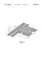
- FIG. 1 shows a schematic representation of one structure optimized for thermal emittance, and adaptable for use with hafnium nitride and zirconium nitride resistive members.
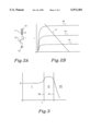
- FIG. 2a shows one possible schematic diagram for a thermal emitting element of the present invention.
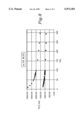
- FIG. 2b shows several I-V (current v. voltage) curves for a MOS device used in a thermal emitting element applicable to the current invention.
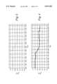
- FIG. 3 shows hypothetical annealing properties for a titanium nitride resistive member.
- FIG. 4 shows the annealing properties for a hafnium nitride resistive member.
- FIG. 5 shows the annealing properties for a zirconium nitride resistive member.
- FIG. 6 shows the temperature stability for a zirconium nitride resistive member subsequent to annealing.
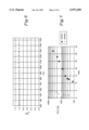
- FIG. 7 shows the nitrogen content vs. resistance properties for zirconium nitride and hafnium nitride resistive members.
- FIG. 8 shows the cryogenic properties for zirconium nitride and hafnium nitride resistive members.
- FIG. 1 shows a typical design for a single thermal emitting element (i.e., pixel) for use in an array of pixels suitable for ohmic heating, and more particularly suitable for production of thermal images.
- a resistive emitting member 1 rests on a silicon nitride bridge or reflector member 2 which may also serve as a thermally isolating member.
- Resistive member 1 is typically, but not necessarily, a long serpentine film (as shown) to maximize its resistance.
- the serpentine shape is combined with thin films (approx. 500 angstroms) having milliohm centimeter resistivities to create pixel resistances of 10K ohms to 100K ohms.
- the serpentine form may be replaced with a restive sheet or other structure if more desirable in a particular circumstance.
- the current controlling means provides binary (i.e. on-off) control of the pixel
- the pixel structure is designed to allow the pixel to emit thermal energy at a number of different levels when the current is varied in a selected operating range.
- the current controlling device is a MOS device
- the current may be controlled by supplying one of a number of gate voltages, each gate voltage resulting in a different pixel temperature. In this way, a user-selected thermal image may be created with the array of pixels.
- the initial value for the resistance of the resistive member is set by doping the resistive member with a material such as nitrogen.
- the resistance of the resistive member increases with increased nitrogen concentrations.
- One typical way of adding nitrogen is to sputter the pixel with nitrogen in a inert atmosphere such as argon. While for the remainder of this application, nitrogen will be used as the doping material, it is to be understood that other doping materials are possible, and may be selected based on specific design needs.
- FIG. 2a shows one possible implementation of the pixel electronics.
- a MOS device 10 serving as the current controlling means, is connected in series with resistive member 11 between two power terminals 12 and 13.
- Resistive member 11 comprises the resistive emitting member 1, the composition of which is the subject of the present invention.
- Three hypothetical characteristic curves, labeled 14, 15, and 16, for MOS device 10 are shown in FIG. 2b. Each curve includes an active region (left-most curved, and semi-vertical portions) and a saturation region (mostly horizontal portions).
- each curve 14, 15 and 16 represents a different gate voltage for MOS device 10.
- I 2 R i.e. resistive
- the current through MOS device 10 and thus through resistive member 11 is roughly proportional to the pixel temperature.
- Each characteristic curve is therefore associated with the pixel at a different temperature.
- the user creates a thermal image by selecting different gate voltages for different pixels to achieve the desired thermal image.
- T sub temperature of the substrate
- G PIX Thermal Conductivity of Pixel to Substrate.
- pixel temperature may be maximized by maximizing power consumption for the pixel.
- the power, P is described by:
- diagonal line 17 in FIG. 2b represents the resistance value of resistive member 11.
- diagonal line 17 should cross the MOS characteristic curve slightly above the active region. Typically, the amount above the active region is about 1 volt, as this prevents the pixel from falling in to the saturation region if there are variations in pixel array voltage. This location for the resistor line maximizes resistance and thus temperature of the resistive member 11, since the slope of the line represents the resistance of resistive member 11.
- an annealing step occurs which stabilizes the pixel for high temperature operation.
- the annealing step may also be used to adjust the resistance of resistive member 11.
- the annealing is done by passing current through the pixel at sufficient levels to cause the pixel to reach the desired anneal temperature.
- the temperature to which the resistive member is annealed determines, at least in part, the operating range of the pixel, and also some of its physical characteristics.
- FIG. 3 shows a hypothetical graph of resistance versus temperature for a titanium nitride resistive member. The location of the curve in the graph shown will vary significantly depending on the nitrogen content of the resistive member and other fabrication factors. The general characteristics of the graph will not change however.
- two dark vertical bars, labeled 20 and 21 represent one possible design choice for the upper and lower boundaries, respectively, of the practical annealing range for a titanium nitride resistive member.
- the region below line 20 has been labeled I
- the region above line 21 has been labeled III.
- the region between lines 20 and 21 is labeled II.
- the designer attempts to heat the pixel to a desired temperature falling within region II.
- region II For most materials, if the pixel is not annealed above vertical bar 20 (region I), the pixel will not have a useful operating temperature range.
- the resistive member could not be operated above the anneal temperature, since operation above that temperature for any length of time would essentially cause the resistive member to further anneal during operation.
- High temperature operation requires operation at least into region II for high resistance materials.
- the pixel's resistance will be difficult to control since resistance drops sharply with increased temperature, and also would not represent the maximum possible resistance capable for the pixel.
- Achieving the proper resistance for the resistive member is complicated by non-uniform temperatures across all the pixels during anneal caused by variations in pixel current, pixel resistance and pixel conductance.
- a material such as titanium nitride with a steep sloping transition from region II to region III makes annealing into region III unattractive. In fact, to prevent accidental annealing into this region III, the designer will typically add a margin of safety before region III, further decreasing the anneal temperature and thus operating range of the pixel.
- resistor line 17 For this reason, the designer must typically adjust the initial position of resistor line 17 for a titanium nitride pixel even further to the right of its optimal position (using a higher nitrogen concentration), so that the resistor line never moves far enough to the left to enter the active region of the MOS curve.
- the nitrogen content of the pixel may be used to place line 20, and thus region I of the graph of FIG. 3, above the desired operating range. While this technique avoids the problem associated with annealing into region II, it unfortunately involves concentrations of nitrogen which make the resistance unacceptably low for some designs.
- hafnium nitride (HfN) and zirconium nitride (ZrN) are relatively stable over the required annealing range, and thus may serve as excellent materials for resistive member 11.
- HfN and ZrN resistive members are formed at much lower nitrogen concentrations. Low nitrogen concentrations create a physically and electronically stronger resistor structure. Devices having resistive members including these materials are also less susceptible to environmental changes.
- the applicants' intended materials for the resistive member may be classified as Group IVB transition metals of the Periodic Table, having forty or more valence electrons.
- FIG. 4 shows a temperature verses resistance curve for a hafnium nitride resistive member
- FIG. 5 shows a similar curve for a zirconium nitride resistive member.
- Neither graph shows a sharp drop in resistance during the upper annealing range, or an initial increase in resistance indicated for Titanium nitride resistive members shown in FIG. 3.
- the resistive member Since there is no higher upper boundary on annealing temperature for the resistive member, there is consequently more flexibility and latitude in the exact temperature of the anneal and in general pixel design. In addition, for low temperature operation, the resistive member shows little or moderate resistance range. This eases the task of annealing because the designer need not worry about the device becoming inoperable during the anneal, such as would be caused by changes in the resistor value pushing the MOS switching member into the active region of operation. Effectively, the hafnium and zirconium nitride exhibit no or minimal transition between what was regions I and II of FIG. 3, or the sharp slope of region III of FIG. 3.
- a hafnium nitride resistive member having nitrogen concentrations of about 10% As can be seen in FIG. 4, resistance decreases from 800 to 1000Kelvin and then stabilizes at a constant value. Annealing performed to just beyond 1000Kelvin produces a temperature stable device.
- a sloping region ends at 1000Kelvin, requiring annealing be done to at least 1000Kelvin to produce a device with good high temperature stability.
- the specific annealing temperatures will shift depending on nitrogen content of the resistive member or other factors.
- Graph 6 shows the resistance vs. temperature for a zirconium nitride resistive member subsequent to annealing. As the graph shows, an annealed resistive member will have a constant, stable resistance to the anneal temperature. For the purposes of this application, resistance temperature stability for the resistive members is defined as less then five percent change in resistance over the operating range of the pixel. A similar graph for hatnium nitride, would also show temperature stability. A similar graph for titanium nitride however, would show loss of temperature stability just above the temperature to which the anneal was performed.
- hafnium nitride and zirconium nitride resistive members operate similarly. There are, however, some differences between these two materials.
- FIG. 7 shows a graph of the resistance of each material for changes in nitrogen content during fabrication.
- a resistive member containing hafnium nitride is much more sensitive to nitrogen content than one containing zirconium nitride. This increases the difficulty of the fabrication process for hafnium nitride, and somewhat for zirconium nitride, since tiny nitrogen content changes cause large resistance changes in the resistive member.
- Hafnium nitride may be chosen over zirconium nitride, despite its heightened sensitivity, if higher resistive values are desired.
- a much higher resistance may be achieved using hafnium nitride with a smaller amount of nitrogen, and this may decrease processing time significantly as well as improving pixel strength.
- Zirconium nitride may be more suitable where exact resistance is more important than a very high resistance value. While exact values for resistance will vary depending on the reader's design criteria, for high temperature operation, nitrogen content for hafnium nitride resistive members would be approximately below ten percent for high temperature operation. Zirconium nitride resistive members should be in the ten to forty percent nitrogen range for high temperature operation. In both cases, the identified nitrogen concentrations will result in a resistance of above about 50 ohms per square for the resistive members.
- films of the resistive member material are typically formed by sputtering Hafnium and Zirconium metals in the presence of a reactive gas, such as nitrogen, and an inert sputtering gas.
- a reactive gas such as nitrogen
- an inert sputtering gas For both hafnium and zirconium nitride resistive members, the nitrogen content must be critically controlled when it is deposited. The applicant has found that the best way to provide a uniform atmosphere of gas at the proper nitrogen content levels during fabrication has been to dilute the nitrogen gas with a much larger portion of carrier gas prior to sputtering. The dilution is typically at one part nitrogen to ten parts carrier gas.
- This carrier gas mixed with the reactive gas is then supplied to the sputtering chamber in addition to the regular supply of sputtering gas supplied to the chamber.
- the sputtering gas is typically, but need not be, the same as the carrier gas.
- the total nitrogen concentration during sputtering is between zero and five percent of the total sputtering gas.
- Ten parts carrier gas to one part nitrogen has been found to produce satisfactory results in the applicant's pixel fabrication process, although higher or lower concentrations may be possible based on the equipment or design used.
- the applicant's preferred carrier gas is Argon due to its inert properties during resistive member processing and usefulness as a sputtering gas.
- the low concentration of nitrogen in a carrier gas corrects for some problems caused by mass flow meters which will not operate at the needed low nitrogen flow rates absent the carrier gas.
- the suggested technique also produces a more uniform nitrogen concentration during the deposition. It is contemplated that use of the carrier gas may be reduced or eliminated when new technology or techniques for proper control of nitrogen flow develop.
- FIG. 8 shows the characteristic resistance of a typical pixel over a temperature range from 20K to 300K. Both materials exhibit relative stability at these cryogenic levels. It is also noted that both of the materials exhibit a small positive thermal coefficient of resistance which is beneficial in preventing thermal runaway for current driven heating such as in the case in the pixel scheme shown in FIG. 1.
- the resistive members may be used as heating elements either individually or as an array. When used in this manner, the resistive member or elements will typically be placed in contact with the material to be heated. A person skilled in the art will recognize further variations that fall within the spirit and scope of the present invention as defined by the following claims.
Abstract
Description
T=P/G.sub.PIX +T.sub.sub, (Equ. 1)
P=I.sup.2 R, (Equ. 2)
Claims (19)
Priority Applications (2)
Application Number | Priority Date | Filing Date | Title |
---|---|---|---|
US09/057,734 US5973383A (en) | 1998-04-09 | 1998-04-09 | High temperature ZrN and HfN IR scene projector pixels |
US09/106,604 US6210494B1 (en) | 1998-04-09 | 1998-06-29 | High temperature ZrN and HfN IR scene projector pixels |
Applications Claiming Priority (1)
Application Number | Priority Date | Filing Date | Title |
---|---|---|---|
US09/057,734 US5973383A (en) | 1998-04-09 | 1998-04-09 | High temperature ZrN and HfN IR scene projector pixels |
Related Child Applications (1)
Application Number | Title | Priority Date | Filing Date |
---|---|---|---|
US09/106,604 Division US6210494B1 (en) | 1998-04-09 | 1998-06-29 | High temperature ZrN and HfN IR scene projector pixels |
Publications (1)
Publication Number | Publication Date |
---|---|
US5973383A true US5973383A (en) | 1999-10-26 |
Family
ID=22012426
Family Applications (2)
Application Number | Title | Priority Date | Filing Date |
---|---|---|---|
US09/057,734 Expired - Lifetime US5973383A (en) | 1998-04-09 | 1998-04-09 | High temperature ZrN and HfN IR scene projector pixels |
US09/106,604 Expired - Lifetime US6210494B1 (en) | 1998-04-09 | 1998-06-29 | High temperature ZrN and HfN IR scene projector pixels |
Family Applications After (1)
Application Number | Title | Priority Date | Filing Date |
---|---|---|---|
US09/106,604 Expired - Lifetime US6210494B1 (en) | 1998-04-09 | 1998-06-29 | High temperature ZrN and HfN IR scene projector pixels |
Country Status (1)
Country | Link |
---|---|
US (2) | US5973383A (en) |
Cited By (11)
Publication number | Priority date | Publication date | Assignee | Title |
---|---|---|---|---|
US6354736B1 (en) * | 1999-03-24 | 2002-03-12 | Honeywell International Inc. | Wide temperature range RTD |
US6627907B1 (en) * | 2000-09-29 | 2003-09-30 | Honeywell International Inc. | Infrared scene projector with current-mirror control electronics |
WO2004048101A1 (en) * | 2002-11-23 | 2004-06-10 | Silverbrook Research Pty Ltd | Thermal ink jet printhead with heaters formed from low atomic number elements |
US20050280672A1 (en) * | 2002-11-23 | 2005-12-22 | Silverbrook Research Pty Ltd. | Printhead nozzle with reduced ink inertia and viscous drag |
US20060055010A1 (en) * | 2004-04-15 | 2006-03-16 | Kheng Lee T | Semiconductor packages |
US7048384B2 (en) | 2003-01-24 | 2006-05-23 | Honeywell International Inc. | Multiple scene projection system |
US20060108587A1 (en) * | 2004-10-26 | 2006-05-25 | Samsung Electronics Co., Ltd. | Thin film transistor array panel and manufacturing method thereof |
US20090030095A1 (en) * | 2007-07-24 | 2009-01-29 | Laverdure Kenneth S | Polystyrene compositions and methods of making and using same |
US20110193066A1 (en) * | 2009-08-13 | 2011-08-11 | E. I. Du Pont De Nemours And Company | Current limiting element for pixels in electronic devices |
US9163995B2 (en) | 2011-10-21 | 2015-10-20 | Santa Barbara Infrared, Inc. | Techniques for tiling arrays of pixel elements |
US9748214B2 (en) | 2011-10-21 | 2017-08-29 | Santa Barbara Infrared, Inc. | Techniques for tiling arrays of pixel elements and fabricating hybridized tiles |
Families Citing this family (4)
Publication number | Priority date | Publication date | Assignee | Title |
---|---|---|---|---|
JP2005018193A (en) * | 2003-06-24 | 2005-01-20 | Hitachi Ltd | Interface command control method for disk device, and computer system |
US9710218B2 (en) | 2014-07-08 | 2017-07-18 | Honeywell International Inc. | Vertical profile display including hazard band indication |
US10037124B2 (en) | 2014-07-08 | 2018-07-31 | Honeywell International Inc. | Vertical profile display including weather icons |
US10495783B2 (en) | 2014-07-08 | 2019-12-03 | Honeywell International Inc. | Vertical profile display including weather blocks |
Citations (5)
Publication number | Priority date | Publication date | Assignee | Title |
---|---|---|---|---|
US5077563A (en) * | 1986-04-10 | 1991-12-31 | Ngk Insulators, Ltd. | Thermally printing head operable with electrically resistive layer provided on printt film or ribbon or on recording medium |
US5286976A (en) * | 1988-11-07 | 1994-02-15 | Honeywell Inc. | Microstructure design for high IR sensitivity |
US5600148A (en) * | 1994-12-30 | 1997-02-04 | Honeywell Inc. | Low power infrared scene projector array and method of manufacture |
US5610637A (en) * | 1992-09-29 | 1997-03-11 | Ricoh Company, Ltd. | Ink jet recording method |
US5777541A (en) * | 1995-08-07 | 1998-07-07 | U.S. Philips Corporation | Multiple element PTC resistor |
Family Cites Families (4)
Publication number | Priority date | Publication date | Assignee | Title |
---|---|---|---|---|
US3647662A (en) * | 1968-02-26 | 1972-03-07 | Bell Telephone Labor Inc | Technique for the fabrication of hafnium nitride resistor |
JPS61127101A (en) * | 1984-11-24 | 1986-06-14 | 日本電信電話株式会社 | Manufacture of high resistance rate zirconium thin film |
JP2789309B2 (en) * | 1995-03-20 | 1998-08-20 | エルジイ・セミコン・カンパニイ・リミテッド | Method for forming refractory metal nitride film |
US6204083B1 (en) | 1996-06-03 | 2001-03-20 | Anritsu Corporation | Process for producing infrared emitting device and infrared emitting device produced by the process |
-
1998
- 1998-04-09 US US09/057,734 patent/US5973383A/en not_active Expired - Lifetime
- 1998-06-29 US US09/106,604 patent/US6210494B1/en not_active Expired - Lifetime
Patent Citations (6)
Publication number | Priority date | Publication date | Assignee | Title |
---|---|---|---|---|
US5077563A (en) * | 1986-04-10 | 1991-12-31 | Ngk Insulators, Ltd. | Thermally printing head operable with electrically resistive layer provided on printt film or ribbon or on recording medium |
US5286976A (en) * | 1988-11-07 | 1994-02-15 | Honeywell Inc. | Microstructure design for high IR sensitivity |
US5610637A (en) * | 1992-09-29 | 1997-03-11 | Ricoh Company, Ltd. | Ink jet recording method |
US5657060A (en) * | 1992-09-29 | 1997-08-12 | Ricoh Company, Ltd. | Ink jet recording head having means for controlling ink droplets |
US5600148A (en) * | 1994-12-30 | 1997-02-04 | Honeywell Inc. | Low power infrared scene projector array and method of manufacture |
US5777541A (en) * | 1995-08-07 | 1998-07-07 | U.S. Philips Corporation | Multiple element PTC resistor |
Non-Patent Citations (14)
Title |
---|
Article entitled "512×512 Infrared Scene Projector Array for Low Background Simulations" by B. E. Cole, C. J. Han, R. E. Higashi, J. Ridley, J. Holmen, J. Anderson, D. Nielsen, H. Marsh, K. Newstrom and C. Zins; Honeywell Technology Center; 10701 Lyndale Ave. S., Bloomington, MN 55420. |
Article entitled "A High Fill Factor Suspended Resistor IR Scene Generator: Design, Fabrication and Preliminary Performance" by A. P. Pritchard, M. C. Hebbron, S. P. Lake and I.M. Sturland; British Aerospace plc Sowerby Research Centre, FPC 267 Filton Bristol BS12 7QW UK; pp. 15-26 from SPIE vol. 1967. |
Article entitled "Dynamic Infrared Scene Projector For Missile Seeker Simulation" by W. S. Chan, J. S. Shie, C. H. Wang, V.K. Raman, Y. C. Chou, T. Karunasiri and R. Frenzel; Electro-Optek Corporation 3152 Kashiwa St., Torrance, CA 90505; pp. 250-255 from Computer Simulation and SPIE, Orlando, FL (1991). |
Article entitled "Dynamic IR Scene Generation: Basic Requirements and Comparative Display Device Design" by A. P. Pritchard; Sowerby Research Centre, British Aerospace plc, FPC 267, Filton, Bristol BS12 7QW, UK; pp. 144-149 from SPIE vol. 940 Infrared Scene Simulation: Systems, Requirements, Calibration, Devices and Modeling (1988). |
Article entitled "Electrically Heated Pixel (EHP) Arrays for Dynamic Infrared Scene Generation" by A. P. Pritchard and S. P. Lake; British Aerospace plc, Sowerby Research Centre (FPC 267); Filton, Bristol, BS12 7QW UK; pp. 182-188 from the SPIE vol. 940 Infrared Scene Simulation: Systems, Requirements, Calibration, Devices, and Modeling (1988). |
Article entitled "Infrared Scene Displays and Their Use in Detector and Processor Assessment" by A. D. Hart, A. P. Pritchard and S. P. Lake; Sowerby Research Centre, Naval Weapons Division, British Aerospace P.L.C., PO Box 5, Filton, Bristol, Great Britain; pp. 153-158 from Infrared Phys. vol. 27, No. 3, 1987. |
Article entitled "Recent Progress in Large Dynamic Resistor Arrays" by B. Cole, R. Higashi, J. Ridley, J. Holmen, and E. Benser; Honeywell Technology Center, 12001 State Highway 55, Plymouth, MN 55441; R. Stockbridge and L. Murrer; Wright Laboratory/MNGI, 101 West Eglin Boulevard, STE 309, Elgin AFB, FL 32542; L. Jones; Science Applications International Corp., 1247-B North Elgin Parkway, Shalimar, Fl 32579 and E. Burroughs; RTTC, STERT-TE-E-SA Bldg. 4500, Redstone Arsenal, AL 35898; pp. 1-13 from SPIE 1997. |
Article entitled 512 512 Infrared Scene Projector Array for Low Background Simulations by B. E. Cole, C. J. Han, R. E. Higashi, J. Ridley, J. Holmen, J. Anderson, D. Nielsen, H. Marsh, K. Newstrom and C. Zins; Honeywell Technology Center; 10701 Lyndale Ave. S., Bloomington, MN 55420. * |
Article entitled A High Fill Factor Suspended Resistor IR Scene Generator: Design, Fabrication and Preliminary Performance by A. P. Pritchard, M. C. Hebbron, S. P. Lake and I.M. Sturland; British Aerospace plc Sowerby Research Centre, FPC 267 Filton Bristol BS12 7QW UK; pp. 15 26 from SPIE vol. 1967. * |
Article entitled Dynamic Infrared Scene Projector For Missile Seeker Simulation by W. S. Chan, J. S. Shie, C. H. Wang, V.K. Raman, Y. C. Chou, T. Karunasiri and R. Frenzel; Electro Optek Corporation 3152 Kashiwa St., Torrance, CA 90505; pp. 250 255 from Computer Simulation and SPIE, Orlando, FL (1991). * |
Article entitled Dynamic IR Scene Generation: Basic Requirements and Comparative Display Device Design by A. P. Pritchard; Sowerby Research Centre, British Aerospace plc, FPC 267, Filton, Bristol BS12 7QW, UK; pp. 144 149 from SPIE vol. 940 Infrared Scene Simulation: Systems, Requirements, Calibration, Devices and Modeling (1988). * |
Article entitled Electrically Heated Pixel (EHP) Arrays for Dynamic Infrared Scene Generation by A. P. Pritchard and S. P. Lake; British Aerospace plc, Sowerby Research Centre (FPC 267); Filton, Bristol, BS12 7QW UK; pp. 182 188 from the SPIE vol. 940 Infrared Scene Simulation: Systems, Requirements, Calibration, Devices, and Modeling (1988). * |
Article entitled Infrared Scene Displays and Their Use in Detector and Processor Assessment by A. D. Hart, A. P. Pritchard and S. P. Lake; Sowerby Research Centre, Naval Weapons Division, British Aerospace P.L.C., PO Box 5, Filton, Bristol, Great Britain; pp. 153 158 from Infrared Phys. vol. 27, No. 3, 1987. * |
Article entitled Recent Progress in Large Dynamic Resistor Arrays by B. Cole, R. Higashi, J. Ridley, J. Holmen, and E. Benser; Honeywell Technology Center, 12001 State Highway 55, Plymouth, MN 55441; R. Stockbridge and L. Murrer; Wright Laboratory/MNGI, 101 West Eglin Boulevard, STE 309, Elgin AFB, FL 32542; L. Jones; Science Applications International Corp., 1247 B North Elgin Parkway, Shalimar, Fl 32579 and E. Burroughs; RTTC, STERT TE E SA Bldg. 4500, Redstone Arsenal, AL 35898; pp. 1 13 from SPIE 1997. * |
Cited By (35)
Publication number | Priority date | Publication date | Assignee | Title |
---|---|---|---|---|
US6354736B1 (en) * | 1999-03-24 | 2002-03-12 | Honeywell International Inc. | Wide temperature range RTD |
US6627907B1 (en) * | 2000-09-29 | 2003-09-30 | Honeywell International Inc. | Infrared scene projector with current-mirror control electronics |
US20080143771A1 (en) * | 2002-11-23 | 2008-06-19 | Silverbrook Research Pty Ltd | Inkjet Printer System With A Pair Of Motor Assemblies |
US7261394B2 (en) | 2002-11-23 | 2007-08-28 | Silverbrook Research Pty Ltd | Inkjet nozzle with reduced fluid inertia and viscous drag |
US6974210B2 (en) | 2002-11-23 | 2005-12-13 | Silverbrook Research Pty Ltd | Thermal ink jet printhead with low density heaters |
US8079678B2 (en) | 2002-11-23 | 2011-12-20 | Silverbrook Research Pty Ltd | Inkjet printhead with nozzles supplied through apertures in the chassis |
AU2003275790B2 (en) * | 2002-11-23 | 2006-03-09 | Zamtec Limited | Thermal ink jet printhead with heaters formed from low atomic number elements |
US20110228000A1 (en) * | 2002-11-23 | 2011-09-22 | Sillverbrook Research Pty Ltd | Printhead Assembly Employing Modular Printheads And Common Substrate Channel |
US20060071982A1 (en) * | 2002-11-23 | 2006-04-06 | Silverbrook Research Pty Ltd | Thermal ink jet printhead with heaters formed from low atomic number elements |
US7533973B2 (en) | 2002-11-23 | 2009-05-19 | Silverbrook Research Pty Ltd | Inkjet printer system with a pair of motor assemblies |
US7967419B2 (en) | 2002-11-23 | 2011-06-28 | Silverbrook Research Pty Ltd | Ink jet printhead incorporating heater element proportionally sized to drop size |
US7147306B2 (en) | 2002-11-23 | 2006-12-12 | Silverbrook Research Pty Ltd | Printhead nozzle with reduced ink inertia and viscous drag |
US20070030312A1 (en) * | 2002-11-23 | 2007-02-08 | Silverbrook Research Pty Ltd | Inkjet nozzle with reduced fluid inertia and viscous drag |
US20100073432A1 (en) * | 2002-11-23 | 2010-03-25 | Silverbrook Research Pty Ltd | Ink Jet Printhead Incorporating Heater Element Proportionally Sized To Drop Size |
US7357489B2 (en) | 2002-11-23 | 2008-04-15 | Silverbrook Research Pty Ltd | Thermal ink jet printhead with heaters formed from low atomic number elements |
US20090195600A1 (en) * | 2002-11-23 | 2009-08-06 | Silverbrook Research Pty Ltd | Inkjet Printhead With Elongate Chassis Defining Ink Supply Apertures |
WO2004048101A1 (en) * | 2002-11-23 | 2004-06-10 | Silverbrook Research Pty Ltd | Thermal ink jet printhead with heaters formed from low atomic number elements |
US20100220158A1 (en) * | 2002-11-23 | 2010-09-02 | Silverbrook Research Pty Ltd | Inkjet printhead with nozzles supplied through apertures in the chassis |
US20050280672A1 (en) * | 2002-11-23 | 2005-12-22 | Silverbrook Research Pty Ltd. | Printhead nozzle with reduced ink inertia and viscous drag |
US20050046676A1 (en) * | 2002-11-23 | 2005-03-03 | Kia Silverbrook | Thermal ink jet printhead with low density heaters |
CN100386200C (en) * | 2002-11-23 | 2008-05-07 | 西尔弗布鲁克研究有限公司 | Thermal ink jet printhead with low density heaters |
US7722169B2 (en) | 2002-11-23 | 2010-05-25 | Silverbrook Research Pty Ltd | Inkjet printhead with elongate chassis defining ink supply apertures |
US7637593B2 (en) | 2002-11-23 | 2009-12-29 | Silverbrook Research Pty Ltd | Printhead with low viscous drag droplet ejection |
US7048384B2 (en) | 2003-01-24 | 2006-05-23 | Honeywell International Inc. | Multiple scene projection system |
US20060055010A1 (en) * | 2004-04-15 | 2006-03-16 | Kheng Lee T | Semiconductor packages |
US20090224254A1 (en) * | 2004-10-26 | 2009-09-10 | Samsung Electronics Co., Ltd. | Thin film transistor array panel and manufacturing method thereof |
US20060108587A1 (en) * | 2004-10-26 | 2006-05-25 | Samsung Electronics Co., Ltd. | Thin film transistor array panel and manufacturing method thereof |
US7527992B2 (en) * | 2004-10-26 | 2009-05-05 | Samsung Electronics Co., Ltd. | Thin film transistor array panel and manufacturing method thereof |
US8207534B2 (en) | 2004-10-26 | 2012-06-26 | Samsung Electronics Co., Ltd. | Thin film transistor array panel and manufacturing method thereof |
US8288771B2 (en) | 2004-10-26 | 2012-10-16 | Samsung Electonics Co., Ltd. | Thin film transistor array panel and manufacturing method thereof |
US8455277B2 (en) | 2004-10-26 | 2013-06-04 | Samsung Display Co., Ltd. | Thin film transistor array panel and manufacturing method thereof |
US20090030095A1 (en) * | 2007-07-24 | 2009-01-29 | Laverdure Kenneth S | Polystyrene compositions and methods of making and using same |
US20110193066A1 (en) * | 2009-08-13 | 2011-08-11 | E. I. Du Pont De Nemours And Company | Current limiting element for pixels in electronic devices |
US9163995B2 (en) | 2011-10-21 | 2015-10-20 | Santa Barbara Infrared, Inc. | Techniques for tiling arrays of pixel elements |
US9748214B2 (en) | 2011-10-21 | 2017-08-29 | Santa Barbara Infrared, Inc. | Techniques for tiling arrays of pixel elements and fabricating hybridized tiles |
Also Published As
Publication number | Publication date |
---|---|
US6210494B1 (en) | 2001-04-03 |
Similar Documents
Publication | Publication Date | Title |
---|---|---|
US5973383A (en) | High temperature ZrN and HfN IR scene projector pixels | |
EP0578883B1 (en) | Diode Lasers | |
US7973384B2 (en) | Phase change memory cell including multiple phase change material portions | |
US5262658A (en) | Thermally stabilized light emitting diode structure | |
US20050029502A1 (en) | Processing phase change material to improve programming speed | |
US8467236B2 (en) | Continuously variable resistor | |
US4553022A (en) | Effusion cell assembly | |
JPH07283392A (en) | Room temperature operation tunnel-hot electron transistor | |
US7268004B2 (en) | Thermoelectric control for field emission display | |
CA2379690C (en) | High temperature zrn and hfn ir scene projector pixels | |
US3651308A (en) | Automatic electric cooker | |
JPH07221346A (en) | Electroluminescent material, semiconductor electroluminescent device and preparation thereof | |
US20040012338A1 (en) | Emitter with dielectric layer having implanted conducting centers | |
US7106120B1 (en) | PCMO resistor trimmer | |
Malyutenko et al. | High temperature (T> 300K) light emitting diodes for 8–12 μm spectral range | |
Cole et al. | Recent progress in large dynamic resistor arrays | |
US3821773A (en) | Solid state emitting device and method of producing the same | |
Moore et al. | Titanium disilicide formation by wide‐area electron beam irradiation | |
US6759260B2 (en) | Metal oxide temperature monitor | |
US4703557A (en) | Adjustment of thick film resistor (TCR) by laser annealing | |
US4246590A (en) | Restoration of high infrared sensitivity in extrinsic silicon detectors | |
JP3328204B2 (en) | Temperature control element | |
EP0378374A3 (en) | Thermal imaging device | |
Shaw | Thermal instability—the precursor to switching in inhomogeneous thin films | |
JP3392885B2 (en) | Electron beam heating apparatus and method |
Legal Events
Date | Code | Title | Description |
---|---|---|---|
AS | Assignment |
Owner name: HONEYWELL INC., MINNESOTA Free format text: ASSIGNMENT OF ASSIGNORS INTEREST;ASSIGNORS:COLE, BARRETT E.;HOLMEN, JAMES O.;GREENLAW, DAVID K.;REEL/FRAME:009196/0193;SIGNING DATES FROM 19980327 TO 19980511 |
|
AS | Assignment |
Owner name: AIR FORCE, UNITED STATES, VIRGINIA Free format text: CONFIRMATORY LICENSE;ASSIGNOR:HONEYWELL, INC.;REEL/FRAME:009248/0435 Effective date: 19980512 |
|
STCF | Information on status: patent grant |
Free format text: PATENTED CASE |
|
AS | Assignment |
Owner name: UNITED STATES AIR FORCE, OHIO Free format text: CONFIRMATORY LICENSE;ASSIGNOR:HONEYWELL INTERNATIONA INCORPORATED;REEL/FRAME:011949/0550 Effective date: 20010504 |
|
FEPP | Fee payment procedure |
Free format text: PAYOR NUMBER ASSIGNED (ORIGINAL EVENT CODE: ASPN); ENTITY STATUS OF PATENT OWNER: LARGE ENTITY |
|
FPAY | Fee payment |
Year of fee payment: 4 |
|
FPAY | Fee payment |
Year of fee payment: 8 |
|
FPAY | Fee payment |
Year of fee payment: 12 |