US5982467A - Method of manufacturing liquid crystal display including active panel - Google Patents
Method of manufacturing liquid crystal display including active panel Download PDFInfo
- Publication number
- US5982467A US5982467A US08/939,813 US93981397A US5982467A US 5982467 A US5982467 A US 5982467A US 93981397 A US93981397 A US 93981397A US 5982467 A US5982467 A US 5982467A
- Authority
- US
- United States
- Prior art keywords
- gate
- forming
- electrode
- source
- contact hole
- Prior art date
- Legal status (The legal status is an assumption and is not a legal conclusion. Google has not performed a legal analysis and makes no representation as to the accuracy of the status listed.)
- Expired - Lifetime
Links
Images


Classifications
-
- G—PHYSICS
- G02—OPTICS
- G02F—OPTICAL DEVICES OR ARRANGEMENTS FOR THE CONTROL OF LIGHT BY MODIFICATION OF THE OPTICAL PROPERTIES OF THE MEDIA OF THE ELEMENTS INVOLVED THEREIN; NON-LINEAR OPTICS; FREQUENCY-CHANGING OF LIGHT; OPTICAL LOGIC ELEMENTS; OPTICAL ANALOGUE/DIGITAL CONVERTERS
- G02F1/00—Devices or arrangements for the control of the intensity, colour, phase, polarisation or direction of light arriving from an independent light source, e.g. switching, gating or modulating; Non-linear optics
- G02F1/01—Devices or arrangements for the control of the intensity, colour, phase, polarisation or direction of light arriving from an independent light source, e.g. switching, gating or modulating; Non-linear optics for the control of the intensity, phase, polarisation or colour
- G02F1/13—Devices or arrangements for the control of the intensity, colour, phase, polarisation or direction of light arriving from an independent light source, e.g. switching, gating or modulating; Non-linear optics for the control of the intensity, phase, polarisation or colour based on liquid crystals, e.g. single liquid crystal display cells
- G02F1/133—Constructional arrangements; Operation of liquid crystal cells; Circuit arrangements
- G02F1/1333—Constructional arrangements; Manufacturing methods
- G02F1/1345—Conductors connecting electrodes to cell terminals
- G02F1/13458—Terminal pads
-
- G—PHYSICS
- G02—OPTICS
- G02F—OPTICAL DEVICES OR ARRANGEMENTS FOR THE CONTROL OF LIGHT BY MODIFICATION OF THE OPTICAL PROPERTIES OF THE MEDIA OF THE ELEMENTS INVOLVED THEREIN; NON-LINEAR OPTICS; FREQUENCY-CHANGING OF LIGHT; OPTICAL LOGIC ELEMENTS; OPTICAL ANALOGUE/DIGITAL CONVERTERS
- G02F1/00—Devices or arrangements for the control of the intensity, colour, phase, polarisation or direction of light arriving from an independent light source, e.g. switching, gating or modulating; Non-linear optics
- G02F1/01—Devices or arrangements for the control of the intensity, colour, phase, polarisation or direction of light arriving from an independent light source, e.g. switching, gating or modulating; Non-linear optics for the control of the intensity, phase, polarisation or colour
- G02F1/13—Devices or arrangements for the control of the intensity, colour, phase, polarisation or direction of light arriving from an independent light source, e.g. switching, gating or modulating; Non-linear optics for the control of the intensity, phase, polarisation or colour based on liquid crystals, e.g. single liquid crystal display cells
- G02F1/133—Constructional arrangements; Operation of liquid crystal cells; Circuit arrangements
- G02F1/136—Liquid crystal cells structurally associated with a semi-conducting layer or substrate, e.g. cells forming part of an integrated circuit
-
- G—PHYSICS
- G02—OPTICS
- G02F—OPTICAL DEVICES OR ARRANGEMENTS FOR THE CONTROL OF LIGHT BY MODIFICATION OF THE OPTICAL PROPERTIES OF THE MEDIA OF THE ELEMENTS INVOLVED THEREIN; NON-LINEAR OPTICS; FREQUENCY-CHANGING OF LIGHT; OPTICAL LOGIC ELEMENTS; OPTICAL ANALOGUE/DIGITAL CONVERTERS
- G02F1/00—Devices or arrangements for the control of the intensity, colour, phase, polarisation or direction of light arriving from an independent light source, e.g. switching, gating or modulating; Non-linear optics
- G02F1/01—Devices or arrangements for the control of the intensity, colour, phase, polarisation or direction of light arriving from an independent light source, e.g. switching, gating or modulating; Non-linear optics for the control of the intensity, phase, polarisation or colour
- G02F1/13—Devices or arrangements for the control of the intensity, colour, phase, polarisation or direction of light arriving from an independent light source, e.g. switching, gating or modulating; Non-linear optics for the control of the intensity, phase, polarisation or colour based on liquid crystals, e.g. single liquid crystal display cells
- G02F1/133—Constructional arrangements; Operation of liquid crystal cells; Circuit arrangements
- G02F1/1333—Constructional arrangements; Manufacturing methods
- G02F1/1343—Electrodes
-
- G—PHYSICS
- G02—OPTICS
- G02F—OPTICAL DEVICES OR ARRANGEMENTS FOR THE CONTROL OF LIGHT BY MODIFICATION OF THE OPTICAL PROPERTIES OF THE MEDIA OF THE ELEMENTS INVOLVED THEREIN; NON-LINEAR OPTICS; FREQUENCY-CHANGING OF LIGHT; OPTICAL LOGIC ELEMENTS; OPTICAL ANALOGUE/DIGITAL CONVERTERS
- G02F1/00—Devices or arrangements for the control of the intensity, colour, phase, polarisation or direction of light arriving from an independent light source, e.g. switching, gating or modulating; Non-linear optics
- G02F1/01—Devices or arrangements for the control of the intensity, colour, phase, polarisation or direction of light arriving from an independent light source, e.g. switching, gating or modulating; Non-linear optics for the control of the intensity, phase, polarisation or colour
- G02F1/13—Devices or arrangements for the control of the intensity, colour, phase, polarisation or direction of light arriving from an independent light source, e.g. switching, gating or modulating; Non-linear optics for the control of the intensity, phase, polarisation or colour based on liquid crystals, e.g. single liquid crystal display cells
- G02F1/133—Constructional arrangements; Operation of liquid crystal cells; Circuit arrangements
- G02F1/136—Liquid crystal cells structurally associated with a semi-conducting layer or substrate, e.g. cells forming part of an integrated circuit
- G02F1/1362—Active matrix addressed cells
- G02F1/136227—Through-hole connection of the pixel electrode to the active element through an insulation layer
-
- G—PHYSICS
- G02—OPTICS
- G02F—OPTICAL DEVICES OR ARRANGEMENTS FOR THE CONTROL OF LIGHT BY MODIFICATION OF THE OPTICAL PROPERTIES OF THE MEDIA OF THE ELEMENTS INVOLVED THEREIN; NON-LINEAR OPTICS; FREQUENCY-CHANGING OF LIGHT; OPTICAL LOGIC ELEMENTS; OPTICAL ANALOGUE/DIGITAL CONVERTERS
- G02F1/00—Devices or arrangements for the control of the intensity, colour, phase, polarisation or direction of light arriving from an independent light source, e.g. switching, gating or modulating; Non-linear optics
- G02F1/01—Devices or arrangements for the control of the intensity, colour, phase, polarisation or direction of light arriving from an independent light source, e.g. switching, gating or modulating; Non-linear optics for the control of the intensity, phase, polarisation or colour
- G02F1/13—Devices or arrangements for the control of the intensity, colour, phase, polarisation or direction of light arriving from an independent light source, e.g. switching, gating or modulating; Non-linear optics for the control of the intensity, phase, polarisation or colour based on liquid crystals, e.g. single liquid crystal display cells
- G02F1/133—Constructional arrangements; Operation of liquid crystal cells; Circuit arrangements
- G02F1/136—Liquid crystal cells structurally associated with a semi-conducting layer or substrate, e.g. cells forming part of an integrated circuit
- G02F1/1362—Active matrix addressed cells
- G02F1/136286—Wiring, e.g. gate line, drain line
-
- G—PHYSICS
- G02—OPTICS
- G02F—OPTICAL DEVICES OR ARRANGEMENTS FOR THE CONTROL OF LIGHT BY MODIFICATION OF THE OPTICAL PROPERTIES OF THE MEDIA OF THE ELEMENTS INVOLVED THEREIN; NON-LINEAR OPTICS; FREQUENCY-CHANGING OF LIGHT; OPTICAL LOGIC ELEMENTS; OPTICAL ANALOGUE/DIGITAL CONVERTERS
- G02F1/00—Devices or arrangements for the control of the intensity, colour, phase, polarisation or direction of light arriving from an independent light source, e.g. switching, gating or modulating; Non-linear optics
- G02F1/01—Devices or arrangements for the control of the intensity, colour, phase, polarisation or direction of light arriving from an independent light source, e.g. switching, gating or modulating; Non-linear optics for the control of the intensity, phase, polarisation or colour
- G02F1/13—Devices or arrangements for the control of the intensity, colour, phase, polarisation or direction of light arriving from an independent light source, e.g. switching, gating or modulating; Non-linear optics for the control of the intensity, phase, polarisation or colour based on liquid crystals, e.g. single liquid crystal display cells
- G02F1/133—Constructional arrangements; Operation of liquid crystal cells; Circuit arrangements
- G02F1/136—Liquid crystal cells structurally associated with a semi-conducting layer or substrate, e.g. cells forming part of an integrated circuit
- G02F1/1362—Active matrix addressed cells
- G02F1/136213—Storage capacitors associated with the pixel electrode
-
- G—PHYSICS
- G02—OPTICS
- G02F—OPTICAL DEVICES OR ARRANGEMENTS FOR THE CONTROL OF LIGHT BY MODIFICATION OF THE OPTICAL PROPERTIES OF THE MEDIA OF THE ELEMENTS INVOLVED THEREIN; NON-LINEAR OPTICS; FREQUENCY-CHANGING OF LIGHT; OPTICAL LOGIC ELEMENTS; OPTICAL ANALOGUE/DIGITAL CONVERTERS
- G02F1/00—Devices or arrangements for the control of the intensity, colour, phase, polarisation or direction of light arriving from an independent light source, e.g. switching, gating or modulating; Non-linear optics
- G02F1/01—Devices or arrangements for the control of the intensity, colour, phase, polarisation or direction of light arriving from an independent light source, e.g. switching, gating or modulating; Non-linear optics for the control of the intensity, phase, polarisation or colour
- G02F1/13—Devices or arrangements for the control of the intensity, colour, phase, polarisation or direction of light arriving from an independent light source, e.g. switching, gating or modulating; Non-linear optics for the control of the intensity, phase, polarisation or colour based on liquid crystals, e.g. single liquid crystal display cells
- G02F1/133—Constructional arrangements; Operation of liquid crystal cells; Circuit arrangements
- G02F1/136—Liquid crystal cells structurally associated with a semi-conducting layer or substrate, e.g. cells forming part of an integrated circuit
- G02F1/1362—Active matrix addressed cells
- G02F1/136286—Wiring, e.g. gate line, drain line
- G02F1/13629—Multilayer wirings
Definitions
- the present invention relates to an active matrix liquid crystal display (AMLCD) including an active panel with thin film transistors (TFT) and pixel electrodes arranged in a matrix pattern, and more particularly, to a simplified method of manufacturing the active panel in the AMLCD.
- AMLCD active matrix liquid crystal display
- TFT thin film transistors
- pixel electrodes arranged in a matrix pattern
- thin film type flat panel display devices are highly favored because of their light weight and easy adaptability.
- active research activities have focused on the development of liquid crystal display devices because of their high resolution and fast response time suitable for display of motion picture images.
- a liquid crystal display device works by using polarization and optical anisotrophy of a liquid crystal. By controlling the orientation of liquid crystal molecules having rod shape through polarization technique, transmission and interception of a light through the liquid crystal are achieved due to the anisotrophy of the liquid crystal. This principle is applied to the liquid crystal display device.
- AMLCDs having TFTs arranged in a matrix pattern and pixel electrodes connected to the TFTs provide high quality images and are now widely used. The structure of a conventional AMLCD will now be described.
- a color filter panel of an LCD includes a sequential arrangement of red, blue and green color filters on a transparent substrate at pixel positions designed in a matrix pattern. Among these color filters, black matrixes are formed in a lattice pattern. On the color filters, a common electrode is formed.
- An active panel of an LCD includes pixel electrodes designed in a matrix pattern and formed on a transparent substrate. Along the column direction of the pixel electrodes, signal bus lines are formed, and along the row direction of the pixel electrodes, data bus lines are formed. At a corner of a pixel electrode, a TFT for driving the pixel electrode is formed. A gate electrode of the TFT is connected with a signal bus line (or a gate bus line). A source electrode of a TFT is connected with a data bus line (or a source bus line). Additionally, a storage capacitor electrode may be formed in parallel with the gate bus line and crossing the pixel electrode. A pad is formed at the end portion of each bus line.
- the color filter panel and the active panel are bonded together with a certain distance therebetween (i.e., a cell gap) to face each other.
- Liquid crystal material fills the cell gap to complete a liquid crystal panel of an LCD.
- the method of manufacturing a liquid crystal display device is very complicated including many processes combined together.
- the method of manufacturing an active panel having TFTs and pixel electrodes is even more complicated. Therefore, it is important to simplify the method for manufacturing an active panel to reduce the possibility of defects during the manufacture process.
- FIG. 1 showing a plan view of an active panel
- FIGS. 2A-2H showing cross-sectional views taken along line II--II of FIG. 1.
- gate bus lines 13 As shown in FIGS. 1 and 2A, aluminum or aluminum alloy is vacuum deposited on a transparent substrate 11 and patterned by using a first mask to form gate bus lines 13, gate pads 15, gate electrodes 17, source pads 25 and a shorting bar 21.
- the gate bus line 13 connects gate electrodes 17 disposed in a column direction.
- the gate pad 15 is disposed at the end of the gate bus line 13.
- the shorting bar 21 makes a connection between the gate pad 15 and the source pad 25 and surrounds the periphery of the substrate 11.
- the source pad 25 is formed at the end portion of source bus lines 23 which are to be formed later.
- the gate bus line 13 may be used for forming a storage capacitor electrode.
- the elements formed of metal as described above are anodized to form an anodic oxide film 13a on the surface. This is to prevent a hill-lock on the aluminum surface. Since the gate electrode 17, gate pad 15, gate bus line 13 and source pad 25 are connected with the shorting bar 21, connection of the shorting bar 21 with an anode facilitates the anodizing of the elements.
- the gate pad 15 and the source pad 25 are covered by using a second mask in order not to form an anodic oxide film on their surfaces.
- silicone oxide or silicone nitride is vacuum deposited on the substrate including the lines and pads to form a gate insulating layer 29. Then, an intrinsic semiconductor material and an impure semiconductor material are deposited sequentially and patterned by using a third mask to form a semiconductor layer 31 and an impure semiconductor layer 33.
- a first gate contact hole 51 on the gate pad 15 and a first source contact hole 61 on the source pad 25 are formed by using a fourth mask.
- the contact holes 51 and 61 expose a portion of the gate pad and a portion of the source pad, respectively, which are not anodized.
- Chromium or chromium alloy is vacuum deposited and patterned by using a fifth mask to form a source electrode 27, a drain electrode 37 and source bus lines 23 on the impure semiconductor layer 33.
- chromium or chromium alloy is also deposited on the gate pad 15 and source pad 25.
- the first source contact hole 61 connects the source bus line 23 with the source pad 25.
- the chromium layer on the source pad is to protect the aluminum layer underneath and is used as an source pad intermediate electrode 67 to connect with a source pad connection terminal 65 which is to be formed later.
- the chromium layer on the gate pad 15 connects the aluminum layer and a gate pad connection terminal 55, which is to be formed later, through the first gate contact hole 51 forming a gate pad intermediate electrode 57.
- the exposed portion of the impure semiconductor 33 between the source electrode 27 and drain electrode 37 is removed by using the source electrode 27 and drain electrode 37 as masks.
- the storage capacitor electrode 19 in (n)th row is formed to overlap the gate line 13 in (n-1)th row.
- an insulating material such as silicone oxide or silicone nitride, is vacuum deposited on the substrate including the source electrode 27 and drain electrode 37 to form a protection layer 35.
- the protection layer 35 is patterned by using a sixth mask to form a second gate contact hole 53 on the gate pad 15, a second source contact hole 63 on the source pad 25, and a drain contact hole 71 on the drain electrode 37.
- the gate pad 15 is connected with an external terminal through the second gate contact hole 53
- the source pad 25 is connected with an external terminal through the second source contact hole 63
- the drain electrode 37 is connected with a pixel electrode 39 (to be formed later) through the drain hole 71.
- the protection layer 35 over the storage capacitor electrode 19 is removed to form a storage capacitor contact hole 75, through which the storage capacitor electrode 19 is connected with the pixel electrode 39.
- part of the shorting bar 21, which is made of aluminum and connected to the gate bus line 13, the gate electrode 17, the gate pad 15 and the source pad 25, is removed to complete the final structure of the active panel by using a seventh mask.
- indium-tin oxide is vacuum deposited on the surface including the protection layer 35 and patterned by using an eighth mask to form pixel electrodes 39, gate pad connection terminals 55 and source pad connection terminals 65.
- the present invention is directed to a liquid crystal display and method that substantially obviates one or more of the problems due to the limitations and disadvantages of the related art.
- An object of the present invention is to provide a method of manufacturing an LCD with less masking steps by eliminating the step of anodizing the gate electrode and the gate bus lines.
- Another object of the present invention is to provide an LCD with reduced accumulated error in the mask arrangement.
- Another object of the present invention is to provide an LCD with increased production yield and enhanced quality.
- a further object of the present invention is to provide an LCD with reduced processing time and cost.
- a method of manufacturing a liquid crystal display device includes the steps of forming a gate bus line on a substrate, using a first metal; forming a gate electrode, a second gate bus line and a gate pad on the substrate having the gate bus line, using a second metal; forming a gate insulating layer on the substrate having the gate bus line, the gate electrode, the gate pad and the second gate bus line, using a first insulating material; forming a semiconductor layer and impure semiconductor layer on the gate insulating layer; forming a source electrode, a drain electrode, a source bus line and a source pad on the substrate having the impure semiconductor layer, using a third metal; removing a portion of the impure semiconductor layer exposed between the source and the drain electrode by etching, using the source and the electrode as masks; forming a protection layer on the substrate having the source and the drain electrode, using a second insulating material; forming a drain
- FIG. 1 is an enlarged plan view showing a part of an active panel of a conventional liquid crystal display device
- FIGS. 2A-2H are cross-sectional views showing the steps of manufacturing an active panel of a conventional liquid crystal display device
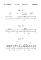
- FIG. 3 is an enlarged plan view showing a part of an active panel of a liquid crystal display device according to a first embodiment of the present invention
- FIGS. 4A-4F are cross-sectional views showing the steps of manufacturing an active panel of a liquid crystal display device according to the first embodiment of the present invention.
- FIGS. 5A-5F are cross-sectional views showing the steps of manufacturing an active panel of a liquid crystal display device according to a second embodiment of the present invention.
- FIG. 6 is an enlarged plan view showing a part of an active panel of a liquid crystal display device according to a third embodiment of the present invention.
- FIGS. 7A-7F are cross-sectional view showing the steps of manufacturing an active panel of a liquid crystal display device according to the third embodiment of the present invention.
- the number of mask steps are reduced to six steps.
- the method according to the present invention eliminates the anodizing process. As a result, it is not necessary to form a shorting bar and cut the shorting bar.
- a source pad is formed during the step of forming a source bus line instead of the step of forming a gate pad. Therefore, a source pad contact hole, connecting the source bus line with the source pad, can be formed directly by patterning a protection layer rather than the two time patterning of the conventional art.
- a gate contact hole, connecting a gate pad with an external terminal can be formed directly by patterning a gate insulating layer and a protection layer simultaneously. As a result, patterning steps such as cutting the shorting bar and forming gate and source pad contact holes can be eliminated.
- the prevention of hill-lock on the aluminum layer is achieved by using a second metal layer covering the aluminum layer instead of anodizing the aluminum layer.
- the gate bus line includes a low resistance metal layer with less surface stability and a high resistance protective metal layer with better surface stability.
- the metal layer for the gate pad and the source pad is connected with the conductive material for the pad connecting terminal.
- a first metal is vacuum deposited on a substrate and patterned by using a first mask to form gate bus lines.
- a second metal is vacuum deposited on the substrate including the gate bus lines and patterned by using a second mask to form gate electrodes and gate pads.
- second gate bus lines are formed above and covering the gate bus lines.
- An insulating material is vacuum deposited on the surface including the gate electrodes, the second gate bus lines and the gate pads to form a gate insulating layer.
- a semiconductor material and an impure semiconductor material are sequentially deposited on the surface of the gate insulating layer and patterned by using a third mask to form a semiconductor layer and an impure semiconductor layer.
- a third metal is vacuum deposited on the surface including the semiconductor layer and patterned by using a fourth mask to form source electrodes, drain electrodes, source bus lines and source pads.
- An insulating material is vacuum deposited on the surface including the source electrodes to form a protection layer.
- a contact hole is formed on the drain electrodes and the source pads, respectively, by removing the protection layer and a contact hole is formed on the gate pads by removing the gate insulating layer and the protection layer.
- a conductive material is vacuum deposited on the resultant surface including the protection layer and patterned by using a sixth mask to form pixel electrodes connected with the drain electrodes, gate pad connecting terminals connected with the gate pads, and source pad connecting terminals connected with the source pads through the contact hole.
- FIGS. 4A-4F are sectional views taken along line IV--IV in FIG. 3
- FIGS. 4A-4F are sectional views taken along line IV--IV in FIG. 3
- gate bus lines 113 As shown in FIG. 4A, aluminum or aluminum alloy is vacuum deposited on a transparent glass substrate 111 and patterned by using a first mask to form gate bus lines 113.
- the gate bus lines 113 may be used to form storage capacitor electrodes.
- a metal such as chromium, molybdenum, tantalum or antimony is vacuum deposited on the substrate including the gate bus lines 113, and patterned by using a second mask to form gate electrodes 117 and gate pads 115 at the end portion of the gate lines 113.
- second gate bus lines 113a are formed to cover the gate bus lines 113 with metal such as chromium, molybdenum, tantalum or antimony to eliminate hill-lock effect on the aluminum surface. Therefore, a shorting bar is not needed in the present invention, since it is not necessary for the gate electrodes 117 and gate bus lines 113 to be anodized.
- an insulating material such as silicone oxide or silicone nitride, is vacuum deposited on the resultant surface including the second gate bus lines 113a to form a gate insulating layer 129.
- a semiconductor material and an impure semiconductor material are vacuum deposited sequentially on the surface of the insulating layer 129 and patterned by using a third mask to form a semiconductor layer 131 and an impure semiconductor layer 133.
- chromium or chromium alloy is vacuum deposited on the insulating layer 129 including the impure semiconductor layer 133, and patterned by using a fourth mask to form source electrodes 127, drain electrodes 137, source bus lines 123, storage electrodes 119 and source pads 125. Subsequently, using the source electrodes 127 and the drain electrodes 137 as masks, the exposed portion of the impure semiconductor layer 133 between the source electrodes 127 and the drain electrodes 137 is removed. As a result, the source electrodes 127 and drain electrodes 137 are formed at opposite positions, respectively, over the gate electrodes 117.
- the source bus lines 123 connect source electrodes 127 formed in a row direction.
- the storage capacitor electrode of the pixel at (n)th row is formed to overlap the gate bus line 113 and the second gate bus line 113a at (n-1)th row.
- an insulating material such as silicone nitride or silicone oxide is vacuum deposited on the surface including the source electrodes 127 and drain electrodes 137 to form a protection layer 135.
- the protection layer 135 is then patterned by using a fifth mask to form a drain contact hole 171 over the drain electrode 137 and a source contact hole 161 over the source pad 125.
- the protection layer 135 and the gate insulating layer 129 over the gate pad are removed to form a gate contact hole 151.
- the protection layer 135 is removed to form a storage capacitor contact hole 175.
- indium-tin oxide is vacuum deposited on the entire resultant surface including the protection layer 135 and patterned by using a sixth mask to form pixel electrodes 139.
- the pixel electrodes 139 are connected with the drain electrode 137 through the drain contact hole 171 and connected with the storage capacitor electrode 119 through the storage capacitor contact hole 175.
- a source pad connecting terminal 165 is formed from the patterned indium-tin oxide layer and connected with the source pad 125 through the source contact hole 161.
- a gate pad connecting o terminal 155 is formed from the patterned indium-tin oxide layer and connected with the gate pad 115 through the gate contact hole 151.
- FIGS. 5A-5F are sectional views taken along line IV--IV in FIG. 3
- the method of manufacturing the active panel of an AMLCD according to a second embodiment of the present invention is described.
- aluminum or aluminum alloy is vacuum deposited on a transparent glass substrate 111 and patterned by using a first mask to form gate bus lines 113, gate electrodes 117 and gate pads 115.
- a metal such as chromium, molybdenum, tantalum or antimony is vacuum deposited on the substrate including the gate bus line 113, gate electrodes 117 and gate pads 115, and patterned by using a second mask to form second gate bus lines 113a, second gate electrodes 117a, and second gate pads 115a covering the gate bus line 113, gate electrodes 117 and gate pads 115, respectively, in order to eliminate hill-lock on the aluminum surface. Therefore, a shorting bar is not needed in the present invention, since it is not necessary for the gate electrodes 117, gate bus lines 113 and gate pads 115 to be anodized.
- an insulating material such as silicone oxide or silicone nitride is vacuum deposited on the resultant surface including the second gate bus lines 113a to form a gate insulating layer 129.
- a semiconductor material and an impure semiconductor material are vacuum deposited sequentially on the surface of the insulating layer 129 and patterned by using a third mask to form a semiconductor layer 131 and an impure semiconductor layer 133.
- chromium or chromium alloy is vacuum deposited on the insulating layer 129 including the impure semiconductor layer 133, and patterned by using a fourth mask to form source electrodes 127, drain electrodes 137, source bus lines 123, storage electrodes 119 and source pads 125. Subsequently, using the source electrodes 127 and the drain electrodes 137 as masks, the exposed portion of the impure semiconductor layer 133 between the source electrodes 127 and the drain electrodes 137 is removed. As a result, the source electrodes 127 and drain electrodes 137 are formed at opposite positions, respectively, over the gate electrodes 117.
- the storage capacitor electrode for the pixel at (n)th row is formed to overlap the gate bus line 113 at (n-1)th row.
- an insulating material such as silicone nitride or silicone oxide is vacuum deposited on the surface including the source electrodes 127 and drain electrodes 137 to form a protection layer 135.
- the protection layer 135 is patterned by using a fifth mask to form a drain contact hole 171 over the drain electrode 137 and a source contact hole 161 over the source pad 125.
- the protection layer 135 and the gate insulating layer 129 over the gate pad are removed to form a gate contact hole 151.
- the protection layer 135 is removed to form a storage capacitor contact hole 175.
- indium-tin oxide is vacuum deposited on the entire resultant surface including the protection layer 135 and patterned by using a sixth mask to form pixel electrodes 139.
- the pixel electrodes 139 are connected with the drain electrode 137 through the drain contact hole 171 and connected with the storage capacitor electrode 119 through the storage capacitor contact hole 175.
- a source pad connecting terminal 165 is formed from the indium-tin oxide material and connected with the source pad 125 through the source contact hole 161.
- a gate pad connecting terminal 155 is formed from the indium-tin oxide material and connected with the gate pad 115 through the gate contact hole 151.
- FIGS. 7A-7F are sectional views taken along line VII--VII in FIG. 6
- FIG. 6 and FIGS. 7A-7F are sectional views taken along line VII--VII in FIG. 6
- the method of manufacturing the active panel of an AMLCD according to a third embodiment of the present invention is described.
- This is an example of a method for forming the storage capacitor line separately in the device of the first embodiment. It is, of course, evident that this can be applied to the method of the second embodiment as well.
- gate bus lines 113 aluminum or aluminum alloy is vacuum deposited on a transparent glass substrate 111 and patterned by using a first mask to form gate bus lines 113.
- storage capacitor lines 141 are formed during the patterning of the aluminum layer, parallel with the gate bus lines 113 and in a position to cross the pixels (see FIG. 6).
- a metal such as chromium, molybdenum, tantalum or antimony is vacuum deposited on the substrate including the gate bus lines 113, and patterned by using a second mask to form gate electrodes 117 and gate pads 115 at the end portion of the gate lines 113.
- second gate bus lines (not shown) are formed to cover the gate bus lines 113 made of aluminum.
- the second gate bus lines are made of metal such as chromium, molybdenum, tantalum or antimony to eliminate hill-lock effect on the aluminum surface.
- second storage capacitor lines 141a are formed to cover the storage capacitor line 141 during the formation of the second gate bus lines. Therefore, a shorting bar is not needed in the present invention, since it is not necessary for the gate electrodes 117 and gate bus lines 113 to be anodized.
- an insulating material such as silicone oxide or silicone nitride is vacuum deposited on the resultant surface including the second gate bus lines 113a, the storage capacitor lines 141 and the second storage capacitor lines 141a to form a gate insulating layer 129.
- a semiconductor material and an impure semiconductor material are vacuum deposited sequentially on the surface of the insulating layer 129 and patterned by using a third mask to form a semiconductor layer 131 and an impure semiconductor layer 133.
- chromium or chromium alloy is vacuum deposited on the insulating layer 129 including the impure semiconductor layer 133, and patterned by using a fourth mask to form source electrodes 127, drain electrodes 137, source bus lines 123, and source pads 125.
- storage capacitor electrodes 119 are formed to overlap the storage capacitor lines 141 and the second storage capacitor lines 141a.
- the exposed portion of the impure semiconductor layer 133 between the source electrodes 127 and the drain electrodes 137 is removed.
- an insulating material such as silicone nitride or silicone oxide is vacuum deposited on the surface including the source electrodes 127 and drain electrodes 137 to form a protection layer 135.
- the protection layer 135 is then patterned by using a fifth mask to form a drain contact hole 171 over the drain electrode 137 and a source contact hole 161 over the source pad 125.
- the protection layer 135 and the gate insulating layer 129 over the gate pad are removed to form a gate contact hole 151.
- the protection layer 135 is removed to form a storage capacitor contact hole 175.
- indium-tin oxide is vacuum deposited on the entire resultant surface including the protection layer 135 and patterned by using a sixth mask to form pixel electrodes 139.
- the pixel electrodes 139 are connected with the drain electrode 137 through the drain contact hole 171 and connected with the storage capacitor electrode 119 through the storage capacitor contact hole 175.
- a source pad connecting terminal 165 is formed from the indium-tin oxide material and connected with the source pad 125 through the source contact hole 161.
- a gate pad connecting terminal 155 is formed from the indium-tin oxide material and connected with the gate pad 115 through the gate contact hole 151.
Abstract
Description
Claims (9)
Priority Applications (1)
| Application Number | Priority Date | Filing Date | Title |
|---|---|---|---|
| US09/305,641 US6088072A (en) | 1996-12-30 | 1999-05-05 | Liquid crystal display having a bus line formed of two metal layers and method of manufacturing the same |
Applications Claiming Priority (2)
| Application Number | Priority Date | Filing Date | Title |
|---|---|---|---|
| KR1019960077958A KR100229613B1 (en) | 1996-12-30 | 1996-12-30 | Lcd device and its manufacturing method |
| KR96-77958 | 1996-12-30 |
Related Child Applications (1)
| Application Number | Title | Priority Date | Filing Date |
|---|---|---|---|
| US09/305,641 Division US6088072A (en) | 1996-12-30 | 1999-05-05 | Liquid crystal display having a bus line formed of two metal layers and method of manufacturing the same |
Publications (1)
| Publication Number | Publication Date |
|---|---|
| US5982467A true US5982467A (en) | 1999-11-09 |
Family
ID=19492733
Family Applications (2)
| Application Number | Title | Priority Date | Filing Date |
|---|---|---|---|
| US08/939,813 Expired - Lifetime US5982467A (en) | 1996-12-30 | 1997-09-29 | Method of manufacturing liquid crystal display including active panel |
| US09/305,641 Expired - Lifetime US6088072A (en) | 1996-12-30 | 1999-05-05 | Liquid crystal display having a bus line formed of two metal layers and method of manufacturing the same |
Family Applications After (1)
| Application Number | Title | Priority Date | Filing Date |
|---|---|---|---|
| US09/305,641 Expired - Lifetime US6088072A (en) | 1996-12-30 | 1999-05-05 | Liquid crystal display having a bus line formed of two metal layers and method of manufacturing the same |
Country Status (6)
| Country | Link |
|---|---|
| US (2) | US5982467A (en) |
| JP (2) | JPH10213809A (en) |
| KR (1) | KR100229613B1 (en) |
| DE (1) | DE19758065C2 (en) |
| FR (1) | FR2758006B1 (en) |
| GB (1) | GB2320766B (en) |
Cited By (20)
| Publication number | Priority date | Publication date | Assignee | Title |
|---|---|---|---|---|
| US6128051A (en) * | 1997-09-12 | 2000-10-03 | Lg Electronics Inc. | Method for forming and apparatus including a liquid crystal display having shorting bar connector |
| US6184948B1 (en) * | 1997-02-11 | 2001-02-06 | Lg Electronics Inc. | Liquid crystal display device having a plurality of error detecting shorting bars and a method of manufacturing the same |
| US20020084459A1 (en) * | 2000-12-29 | 2002-07-04 | Choi Seung Kyu | Thin film transistor substrate and fabricating method thereof |
| US20020093599A1 (en) * | 2000-12-29 | 2002-07-18 | Ha Young Hun | Liquid crystal display and fabricating method thereof |
| US6567135B1 (en) * | 1999-07-31 | 2003-05-20 | Lg. Philips Lcd Co., Ltd. | Liquid crystal display device and method for fabricating the same |
| WO2003058332A1 (en) * | 2002-01-14 | 2003-07-17 | Samsung Electronics Co., Ltd. | Reflection type liquid crystal display device and method of manufacturing the same |
| US6621544B2 (en) * | 2000-10-20 | 2003-09-16 | Sharp Kabushiki Kaisha | Liquid crystal display apparatus and projection-type liquid crystal display apparatus |
| US6633058B1 (en) * | 1999-07-26 | 2003-10-14 | Dalsa, Inc. | Variable reticulation time delay and integrate sensor |
| US20040159630A1 (en) * | 2003-02-14 | 2004-08-19 | Lu-Kuen Chang | Method for forming a liquid crystal display panel |
| US6900871B1 (en) * | 2000-02-24 | 2005-05-31 | Lg. Philips Lcd Co. Ltd. | Thin film transistor substrate of liquid crystal display and method of manufacture |
| US6949417B1 (en) * | 1997-03-05 | 2005-09-27 | Lg. Philips Lcd Co., Ltd. | Liquid crystal display and method of manufacturing the same |
| CN1303467C (en) * | 2003-04-11 | 2007-03-07 | 广辉电子股份有限公司 | Method for making liquid crystal display panel |
| US20070159564A1 (en) * | 2005-12-16 | 2007-07-12 | Innolux Display Corp. | Thin film transistor substrate of liquid crystal display and method for fabricating the same |
| US20070200984A1 (en) * | 2003-09-03 | 2007-08-30 | Jeong-Ho Lee | Reflection type liquid crystal display device and method of manufacturing the same |
| CN100371819C (en) * | 2003-10-14 | 2008-02-27 | Lg.菲利浦Lcd株式会社 | Liquid crystal display panel and fabricating method thereof |
| CN100407428C (en) * | 2002-02-12 | 2008-07-30 | 精工爱普生株式会社 | Thin film semiconductor device, electrolight device and intermediate mask |
| US20110248274A1 (en) * | 1998-11-26 | 2011-10-13 | Dong-Gyu Kim | Thin film transistor array panel for liquid crystal display and method of manufacturing the same |
| US9859351B2 (en) * | 2014-09-30 | 2018-01-02 | Sansung Display Co., LTD. | Organic light-emitting diode display |
| CN108153072A (en) * | 2018-01-02 | 2018-06-12 | 京东方科技集团股份有限公司 | Array substrate and preparation method thereof, display device |
| US10268095B2 (en) * | 2016-01-25 | 2019-04-23 | Wuhan China Star Optoelectronics Co., Ltd | Array substrate, liquid crystal display panel and liquid crystal display device |
Families Citing this family (27)
| Publication number | Priority date | Publication date | Assignee | Title |
|---|---|---|---|---|
| KR100262954B1 (en) * | 1997-09-03 | 2000-08-01 | 구본준 | Lcd manufacturing method and structure by the same method |
| KR100271037B1 (en) * | 1997-09-05 | 2000-11-01 | 구본준, 론 위라하디락사 | Structure and fabrication method of lcd |
| KR100276442B1 (en) * | 1998-02-20 | 2000-12-15 | 구본준 | Liquid crystal display device and its fabrication method |
| KR20000027776A (en) * | 1998-10-29 | 2000-05-15 | 김영환 | Method for manufacturing lcd |
| KR100293985B1 (en) * | 1998-11-26 | 2001-07-12 | 윤종용 | Thin film transistor substrate for liquid crystal display device with improved pad reliability and manufacturing method |
| JP4004672B2 (en) * | 1998-12-28 | 2007-11-07 | シャープ株式会社 | Substrate for liquid crystal display device and manufacturing method thereof |
| US6448579B1 (en) * | 2000-12-06 | 2002-09-10 | L.G.Philips Lcd Co., Ltd. | Thin film transistor array substrate for liquid crystal display and a method for fabricating the same |
| JP3391343B2 (en) * | 1999-10-26 | 2003-03-31 | 日本電気株式会社 | Active matrix substrate and manufacturing method thereof |
| JP2001343659A (en) * | 2000-06-02 | 2001-12-14 | Casio Comput Co Ltd | Active matrix type liquid crystal display panel and method of manufacture |
| KR100796749B1 (en) * | 2001-05-16 | 2008-01-22 | 삼성전자주식회사 | A thin film transistor array substrate for a liquid crystal display |
| KR100840318B1 (en) * | 2001-12-10 | 2008-06-20 | 삼성전자주식회사 | Thin film transistor substrate, fabricating method thereof and liquid crystal display |
| US7209192B2 (en) * | 2001-09-26 | 2007-04-24 | Samsung Electronics Co., Ltd. | Thin film transistor array panel for liquid crystal display and method for manufacturing the same |
| US6933529B2 (en) * | 2002-07-11 | 2005-08-23 | Lg. Philips Lcd Co., Ltd. | Active matrix type organic light emitting diode device and thin film transistor thereof |
| TWI242671B (en) * | 2003-03-29 | 2005-11-01 | Lg Philips Lcd Co Ltd | Liquid crystal display of horizontal electronic field applying type and fabricating method thereof |
| KR100532087B1 (en) * | 2003-06-20 | 2005-11-30 | 엘지.필립스 엘시디 주식회사 | Liquid crystal display device |
| KR100560400B1 (en) * | 2003-11-04 | 2006-03-14 | 엘지.필립스 엘시디 주식회사 | Thin film transistor substrate of horizontal electronic field applying type and fabricating method thereof |
| KR101050300B1 (en) * | 2004-07-30 | 2011-07-19 | 엘지디스플레이 주식회사 | Array substrate for liquid crystal display apparatus and manufacturing method thereof |
| KR101133758B1 (en) * | 2005-01-19 | 2012-04-09 | 삼성전자주식회사 | Sensor and thin film transistor array panel including sensor |
| KR101085450B1 (en) * | 2005-02-07 | 2011-11-21 | 삼성전자주식회사 | Tft substrate and manufacturing method of the same |
| KR101213871B1 (en) * | 2005-12-15 | 2012-12-18 | 엘지디스플레이 주식회사 | Thin film transistor array substrate and manufacturing method of the same |
| JP2008047932A (en) * | 2007-09-18 | 2008-02-28 | Nec Lcd Technologies Ltd | Method of manufacturing thin-film transistor |
| JP2009122244A (en) * | 2007-11-13 | 2009-06-04 | Mitsubishi Electric Corp | Method of manufacturing thin film transistor array substrate, and display device |
| US9041202B2 (en) * | 2008-05-16 | 2015-05-26 | Semiconductor Energy Laboratory Co., Ltd. | Semiconductor device and manufacturing method of the same |
| US20100224880A1 (en) * | 2009-03-05 | 2010-09-09 | Semiconductor Energy Laboratory Co., Ltd. | Semiconductor device |
| TWI413839B (en) * | 2009-03-24 | 2013-11-01 | Hannstar Display Corp | Pixel element of liquid crystal display and method for roducing the same |
| JP5988380B2 (en) * | 2010-12-24 | 2016-09-07 | Necライティング株式会社 | ORGANIC ELECTROLUMINESCENT ELEMENT AND ORGANIC ELECTROLUMINESCENT LIGHTING DEVICE |
| JP2012208294A (en) * | 2011-03-29 | 2012-10-25 | Seiko Epson Corp | Method for manufacturing electro-optic device, electro-optic device, projection-type display device, and electronic equipment |
Citations (3)
| Publication number | Priority date | Publication date | Assignee | Title |
|---|---|---|---|---|
| US5055899A (en) * | 1987-09-09 | 1991-10-08 | Casio Computer Co., Ltd. | Thin film transistor |
| US5334860A (en) * | 1991-06-27 | 1994-08-02 | Casio Computer Co., Ltd. | Panel having thin film element formed thereon |
| US5731856A (en) * | 1995-12-30 | 1998-03-24 | Samsung Electronics Co., Ltd. | Methods for forming liquid crystal displays including thin film transistors and gate pads having a particular structure |
Family Cites Families (17)
| Publication number | Priority date | Publication date | Assignee | Title |
|---|---|---|---|---|
| JPH07113726B2 (en) * | 1989-01-10 | 1995-12-06 | 富士通株式会社 | Method of manufacturing thin film transistor matrix |
| JPH0828517B2 (en) * | 1989-07-04 | 1996-03-21 | シャープ株式会社 | Thin film transistor array |
| JPH0338620A (en) * | 1989-07-05 | 1991-02-19 | Sharp Corp | Active matrix substrate |
| JPH0341774A (en) * | 1989-07-10 | 1991-02-22 | Sharp Corp | Thin film transistor |
| US5498573A (en) * | 1989-11-29 | 1996-03-12 | General Electric Company | Method of making multi-layer address lines for amorphous silicon liquid crystal display devices |
| KR940000143B1 (en) * | 1991-06-25 | 1994-01-07 | 재단법인 한국전자통신연구소 | Method of making large tft-lcd panel |
| KR950010661B1 (en) * | 1992-11-07 | 1995-09-21 | 엘지전자주식회사 | Manufacturing method of and structure of a signal line in use for tft lcd |
| JP3098345B2 (en) * | 1992-12-28 | 2000-10-16 | 富士通株式会社 | Thin film transistor matrix device and method of manufacturing the same |
| JPH06267986A (en) * | 1993-03-17 | 1994-09-22 | Hitachi Ltd | Method of manufacturing thin film transistor |
| DE4339721C1 (en) * | 1993-11-22 | 1995-02-02 | Lueder Ernst | Method for producing a matrix of thin-film transistors |
| JP3281167B2 (en) * | 1994-03-17 | 2002-05-13 | 富士通株式会社 | Method for manufacturing thin film transistor |
| US5518805A (en) * | 1994-04-28 | 1996-05-21 | Xerox Corporation | Hillock-free multilayer metal lines for high performance thin film structures |
| JPH08116065A (en) * | 1994-10-12 | 1996-05-07 | Sony Corp | Thin film semiconductor device |
| JPH08179362A (en) * | 1994-12-22 | 1996-07-12 | Mitsubishi Electric Corp | Thin-film transistor array substrate |
| KR0175409B1 (en) * | 1995-11-20 | 1999-02-18 | 김광호 | Method of making a tft panel for lcd |
| DE69635239T2 (en) * | 1995-11-21 | 2006-07-06 | Samsung Electronics Co., Ltd., Suwon | Process for producing a liquid crystal display |
| JPH09153623A (en) * | 1995-11-30 | 1997-06-10 | Sony Corp | Thin film semiconductor device |
-
1996
- 1996-12-30 KR KR1019960077958A patent/KR100229613B1/en active IP Right Grant
-
1997
- 1997-09-29 US US08/939,813 patent/US5982467A/en not_active Expired - Lifetime
- 1997-12-18 JP JP9348776A patent/JPH10213809A/en not_active Abandoned
- 1997-12-26 FR FR9716573A patent/FR2758006B1/en not_active Expired - Lifetime
- 1997-12-29 DE DE19758065A patent/DE19758065C2/en not_active Expired - Lifetime
- 1997-12-30 GB GB9727477A patent/GB2320766B/en not_active Expired - Lifetime
-
1999
- 1999-05-05 US US09/305,641 patent/US6088072A/en not_active Expired - Lifetime
-
2010
- 2010-01-19 JP JP2010008965A patent/JP2010108000A/en active Pending
Patent Citations (3)
| Publication number | Priority date | Publication date | Assignee | Title |
|---|---|---|---|---|
| US5055899A (en) * | 1987-09-09 | 1991-10-08 | Casio Computer Co., Ltd. | Thin film transistor |
| US5334860A (en) * | 1991-06-27 | 1994-08-02 | Casio Computer Co., Ltd. | Panel having thin film element formed thereon |
| US5731856A (en) * | 1995-12-30 | 1998-03-24 | Samsung Electronics Co., Ltd. | Methods for forming liquid crystal displays including thin film transistors and gate pads having a particular structure |
Cited By (31)
| Publication number | Priority date | Publication date | Assignee | Title |
|---|---|---|---|---|
| US6184948B1 (en) * | 1997-02-11 | 2001-02-06 | Lg Electronics Inc. | Liquid crystal display device having a plurality of error detecting shorting bars and a method of manufacturing the same |
| US6949417B1 (en) * | 1997-03-05 | 2005-09-27 | Lg. Philips Lcd Co., Ltd. | Liquid crystal display and method of manufacturing the same |
| US7462516B2 (en) | 1997-03-05 | 2008-12-09 | Lg Display Co., Ltd. | Liquid crystal display and method of manufacturing the same |
| US20050282303A1 (en) * | 1997-03-05 | 2005-12-22 | Ahn Byung C | Liquid crystal display and method of manufacturing the same |
| US6128051A (en) * | 1997-09-12 | 2000-10-03 | Lg Electronics Inc. | Method for forming and apparatus including a liquid crystal display having shorting bar connector |
| US20110248274A1 (en) * | 1998-11-26 | 2011-10-13 | Dong-Gyu Kim | Thin film transistor array panel for liquid crystal display and method of manufacturing the same |
| US8294839B2 (en) * | 1998-11-26 | 2012-10-23 | Samsung Display Co., Ltd. | Thin film transistor array panel for liquid crystal display and method of manufacturing the same |
| US6633058B1 (en) * | 1999-07-26 | 2003-10-14 | Dalsa, Inc. | Variable reticulation time delay and integrate sensor |
| US6567135B1 (en) * | 1999-07-31 | 2003-05-20 | Lg. Philips Lcd Co., Ltd. | Liquid crystal display device and method for fabricating the same |
| US6900871B1 (en) * | 2000-02-24 | 2005-05-31 | Lg. Philips Lcd Co. Ltd. | Thin film transistor substrate of liquid crystal display and method of manufacture |
| US6621544B2 (en) * | 2000-10-20 | 2003-09-16 | Sharp Kabushiki Kaisha | Liquid crystal display apparatus and projection-type liquid crystal display apparatus |
| US7106390B2 (en) * | 2000-12-29 | 2006-09-12 | Lg.Philips Lcd Co., Ltd. | Liquid crystal display and fabricating method thereof |
| US6921917B2 (en) * | 2000-12-29 | 2005-07-26 | Lg. Philips Lcd Co., Ltd. | Thin film transistor substrate and fabricating method thereof |
| US20020093599A1 (en) * | 2000-12-29 | 2002-07-18 | Ha Young Hun | Liquid crystal display and fabricating method thereof |
| US20020084459A1 (en) * | 2000-12-29 | 2002-07-04 | Choi Seung Kyu | Thin film transistor substrate and fabricating method thereof |
| US20050088591A1 (en) * | 2002-01-14 | 2005-04-28 | Jeong-Ho Lee | Reflection type liquid crystal display device and method of manufacturing the same |
| WO2003058332A1 (en) * | 2002-01-14 | 2003-07-17 | Samsung Electronics Co., Ltd. | Reflection type liquid crystal display device and method of manufacturing the same |
| CN100346217C (en) * | 2002-01-14 | 2007-10-31 | 三星电子株式会社 | Reflection type liquid crystal display device and method of manufacturing the same |
| US7230668B2 (en) | 2002-01-14 | 2007-06-12 | Samsung Electronics Co., Inc. | Reflection type liquid crystal display device with a passivation layer directly on the pad electrode |
| CN100407428C (en) * | 2002-02-12 | 2008-07-30 | 精工爱普生株式会社 | Thin film semiconductor device, electrolight device and intermediate mask |
| US7060195B2 (en) * | 2003-02-14 | 2006-06-13 | Quanta Display Inc. | Method for forming a liquid crystal display panel |
| US20040159630A1 (en) * | 2003-02-14 | 2004-08-19 | Lu-Kuen Chang | Method for forming a liquid crystal display panel |
| CN1303467C (en) * | 2003-04-11 | 2007-03-07 | 广辉电子股份有限公司 | Method for making liquid crystal display panel |
| US20070200984A1 (en) * | 2003-09-03 | 2007-08-30 | Jeong-Ho Lee | Reflection type liquid crystal display device and method of manufacturing the same |
| CN100371819C (en) * | 2003-10-14 | 2008-02-27 | Lg.菲利浦Lcd株式会社 | Liquid crystal display panel and fabricating method thereof |
| US20070159564A1 (en) * | 2005-12-16 | 2007-07-12 | Innolux Display Corp. | Thin film transistor substrate of liquid crystal display and method for fabricating the same |
| US9859351B2 (en) * | 2014-09-30 | 2018-01-02 | Sansung Display Co., LTD. | Organic light-emitting diode display |
| US10268095B2 (en) * | 2016-01-25 | 2019-04-23 | Wuhan China Star Optoelectronics Co., Ltd | Array substrate, liquid crystal display panel and liquid crystal display device |
| US10288967B2 (en) * | 2016-01-25 | 2019-05-14 | Wuhan China Star Optoelectronics Technology Co., Ltd | Array substrate, liquid crystal display panel and liquid crystal display device |
| US10324348B2 (en) * | 2016-01-25 | 2019-06-18 | Wuhan China Star Optoelectronics Technologies Co., Ltd | Array substrate, liquid crystal display panel and liquid crystal display device |
| CN108153072A (en) * | 2018-01-02 | 2018-06-12 | 京东方科技集团股份有限公司 | Array substrate and preparation method thereof, display device |
Also Published As
| Publication number | Publication date |
|---|---|
| DE19758065C2 (en) | 2002-04-18 |
| JPH10213809A (en) | 1998-08-11 |
| JP2010108000A (en) | 2010-05-13 |
| GB2320766B (en) | 1999-08-11 |
| DE19758065A1 (en) | 1998-07-02 |
| FR2758006A1 (en) | 1998-07-03 |
| GB9727477D0 (en) | 1998-02-25 |
| GB2320766A (en) | 1998-07-01 |
| KR100229613B1 (en) | 1999-11-15 |
| KR19980058630A (en) | 1998-10-07 |
| FR2758006B1 (en) | 2003-04-04 |
| US6088072A (en) | 2000-07-11 |
Similar Documents
| Publication | Publication Date | Title |
|---|---|---|
| US5982467A (en) | Method of manufacturing liquid crystal display including active panel | |
| US6614500B2 (en) | Liquid crystal display having a dummy source pad and method for manufacturing the same | |
| US6038003A (en) | Liquid crystal display and method of manufacturing the same | |
| KR100244447B1 (en) | Liquid crystal display and method for manufacturing the same | |
| JP4364952B2 (en) | Manufacturing method of liquid crystal display device | |
| US6184948B1 (en) | Liquid crystal display device having a plurality of error detecting shorting bars and a method of manufacturing the same | |
| US6128051A (en) | Method for forming and apparatus including a liquid crystal display having shorting bar connector | |
| KR100307385B1 (en) | Structure of lcd and manufacturing method of lcd | |
| JP4266793B2 (en) | Array substrate for liquid crystal display | |
| US20040001170A1 (en) | Liquid crystal display device having array substrate of color filter on thin film transistor structure and manufacturing method thereof | |
| JPH03288824A (en) | Active matrix display device | |
| KR19980018480A (en) | LCD Display | |
| US6330042B1 (en) | Liquid crystal display and the method of manufacturing the same | |
| KR100942265B1 (en) | LCD with color-filter on TFT and method of fabricating of the same | |
| KR100482167B1 (en) | LCD and its manufacturing method | |
| KR20020013787A (en) | Liquid crystal display device and method for manufacturing the same | |
| KR20000019504A (en) | Method for manufacturing lcd | |
| KR100959366B1 (en) | Array Substrate of Liquid Crystal Display Device Having Color Filter on Thin Film Transistor COT Structure and Method for Fabricating the Same | |
| KR100235594B1 (en) | Liquid crystal display and method for manufacturing the same | |
| KR100926433B1 (en) | Liquid Crystal Display and the Fabrication method | |
| JP3323880B2 (en) | Liquid crystal display | |
| KR100235593B1 (en) | Liquid crystal display and method for manufacturing the same | |
| KR100514764B1 (en) | Liquid crystal display device and the method for manufaturing the same | |
| KR100252307B1 (en) | Method for manufacturing lcd and the structure by the same method | |
| JP3508964B2 (en) | Liquid crystal display device and manufacturing method thereof |
Legal Events
| Date | Code | Title | Description |
|---|---|---|---|
| AS | Assignment |
Owner name: LG ELECTRONICS, KOREA, REPUBLIC OF Free format text: (ASSIGNMENT OF ASSIGNOR'S INTEREST) RE-RECORD TO CORRECT THE RECORDATION DATE OF 12/10/97 TO 09/29/97 PREVIOUSLY RECORDED AT REEL 8827, FRAME 0741;ASSIGNOR:LEE, SEONG SU;REEL/FRAME:009174/0216 Effective date: 19970722 |
|
| AS | Assignment |
Owner name: LG ELECTRONICS, KOREA, REPUBLIC OF Free format text: ;ASSIGNOR:LEE, SEONG SU;REEL/FRAME:008827/0741 Effective date: 19970722 |
|
| AS | Assignment |
Owner name: LG. PHILIPS LCD CO., LTD., KOREA, DEMOCRATIC PEOPL Free format text: ASSIGNMENT OF ASSIGNORS INTEREST;ASSIGNOR:LG ELECTRONICS, INC.;REEL/FRAME:010281/0291 Effective date: 19990921 |
|
| STCF | Information on status: patent grant |
Free format text: PATENTED CASE |
|
| FEPP | Fee payment procedure |
Free format text: PAYOR NUMBER ASSIGNED (ORIGINAL EVENT CODE: ASPN); ENTITY STATUS OF PATENT OWNER: LARGE ENTITY |
|
| FPAY | Fee payment |
Year of fee payment: 4 |
|
| FPAY | Fee payment |
Year of fee payment: 8 |
|
| AS | Assignment |
Owner name: LG.PHILIPS LCD CO., LTD., KOREA, REPUBLIC OF Free format text: ASSIGNMENT OF ASSIGNORS INTEREST;ASSIGNOR:LG ELECTRONICS INC.;REEL/FRAME:020385/0124 Effective date: 19990921 |
|
| AS | Assignment |
Owner name: LG DISPLAY CO., LTD., KOREA, REPUBLIC OF Free format text: CHANGE OF NAME;ASSIGNOR:LG.PHILIPS LCD CO., LTD.;REEL/FRAME:021754/0230 Effective date: 20080304 Owner name: LG DISPLAY CO., LTD.,KOREA, REPUBLIC OF Free format text: CHANGE OF NAME;ASSIGNOR:LG.PHILIPS LCD CO., LTD.;REEL/FRAME:021754/0230 Effective date: 20080304 |
|
| FEPP | Fee payment procedure |
Free format text: PAYOR NUMBER ASSIGNED (ORIGINAL EVENT CODE: ASPN); ENTITY STATUS OF PATENT OWNER: LARGE ENTITY Free format text: PAYER NUMBER DE-ASSIGNED (ORIGINAL EVENT CODE: RMPN); ENTITY STATUS OF PATENT OWNER: LARGE ENTITY |
|
| FPAY | Fee payment |
Year of fee payment: 12 |