US5986615A - Antenna with ground plane having cutouts - Google Patents
Antenna with ground plane having cutouts Download PDFInfo
- Publication number
- US5986615A US5986615A US08/934,146 US93414697A US5986615A US 5986615 A US5986615 A US 5986615A US 93414697 A US93414697 A US 93414697A US 5986615 A US5986615 A US 5986615A
- Authority
- US
- United States
- Prior art keywords
- antenna structure
- structure according
- ground plane
- central region
- cutouts
- Prior art date
- Legal status (The legal status is an assumption and is not a legal conclusion. Google has not performed a legal analysis and makes no representation as to the accuracy of the status listed.)
- Expired - Lifetime
Links
Images


Classifications
-
- H—ELECTRICITY
- H01—ELECTRIC ELEMENTS
- H01Q—ANTENNAS, i.e. RADIO AERIALS
- H01Q1/00—Details of, or arrangements associated with, antennas
- H01Q1/48—Earthing means; Earth screens; Counterpoises
Definitions
- This invention relates to antenna structures and more particularly to a novel and highly effective antenna structure comprising a radiating element such as a patch antenna in combination with a ground plane constructed to enhance antenna performance.
- Antenna structures known heretofore that are capable of optimum performance are too bulky and unwieldy for use in small GPS receivers, especially hand-held receivers.
- Compact antenna structures that are conventionally employed with GPS receivers do not provide optimum performance.
- One problem is that they receive signals directly from satellites and, because of ground reflections, also indirectly. This so-called multipath reception causes time measurement errors that can lead to a geographical fix that is erroneous or at least suspect.
- a British patent publication No. 2,057,773 of Marconi discloses a large radio transmitting antenna including aerial wires supported in spaced, parallel relation by posts.
- the ground around the antenna is saturated to a depth of two or three meters with an aqueous solution of calcium sulfate to increase the conductivity of the ground and thereby improve its reflectivity.
- the ground is permeated to a distance two to three times as far from the antenna as the antenna is tall. In a typical case this can be from 50 to 100 meters from the boundaries of the antenna array.
- a European patent publication No. 394,960 of Kokusai Denshin Denwa discloses a microstrip antenna having a radiation conductor and a ground conductor on opposite sides of a dielectric substrate.
- the spacing between the radiation conductor and the ground conductor, or the thickness of the dielectric substrate, is larger at the peripheral portion of those conductors than at the central portion. Because of the large spacing at the peripheral portion, the impedance at the peripheral portion where electromagnetic waves are radiated is said to be close to the free-space impedance.
- a German patent publication No. DE 37 38 513 and its U.S. counterpart U.S. Pat. No. 5,061,938 to Zahn et al. disclose a microstrip antenna including an electrically conductive base plate carrying an electrically insulating substrate on top of which are a plurality of radiating patches.
- a relatively large spacing is established between the electrically insulating substrate and the base plate at lateral dimensions somewhat larger than lateral dimensions of the patches and also in the vicinity of the patches.
- the patches and spacings are vertically aligned through either local elevations of the insulating substrate or local indentations in the base plate.
- the feeder line is thus relatively close to the conductive base plate, and the radiating patch is farther away from the conductive base plate. This is said to improve the radiating characteristics of the patch.
- German patent publication No. DE 43 26 117 of Fischer discloses a cordless telephone with an improved antenna.
- a European patent publication No. 318,873 of Toppan Printing Co., Ltd., and Seiko Instruments Inc. discloses an electromagnetic-wave-absorbing element comprising an elongate rectangular body of dielectric material having a bottom portion attachable to an inner wall of an electromagnetically dark room, and peripheral elongate faces extending vertically from the bottom portion.
- a set of the absorbing elements can be arranged in rows and columns on the wall.
- An electroconductive ink film is formed on the peripheral faces of the body and has a gradually changing surface resistivity decreasing exponentially lengthwise of the peripheral face toward the bottom portion.
- the incident electromagnetic wave normal to the wall provided with the rows and columns of absorbing elements is absorbed by a lattice of the electroconductive film during the travel along the electroconductive film.
- the characteristic impedance at the top of the element through which the incident wave enters is close to the impedance of air.
- the characteristic impedance at the bottom is close to that of the wall.
- the absorbing element is made of a plastic body with an electroconductive covering and having a variable resistivity or conductivity.
- An object of the invention is to overcome the problems of the prior art noted above and in particular to provide an antenna structure that reduces multipath signals caused by reflection from the earth, that is physically small yet simulates an infinite ground plane, and that is particularly adapted for use in a GPS receiver that receives and processes signals from navigation satellites.
- Another object of the invention is to provide an antenna structure that is suitable for hand-held units of the type used by surveyors.
- an antenna structure comprising a radiating element and a ground plane for the radiating element having a central region closely spaced apart from the radiating element and a peripheral region extending away from the central region.
- the peripheral region is formed with at least one cutout having an area that increases as radial distance from the central region increases to provide an equivalent sheet resistivity that increases as radial distance from the central region increases.
- a method comprising the steps of forming an antenna structure comprising a radiating element for receiving broadcast signals directly and, because of reflection of the signals, also indirectly with a time delay, and a ground plane.
- the ground plane has a central region closely spaced apart from the radiating element and a peripheral region extending away from the central region.
- the peripheral region is formed with at least one cutout having an area that increases as radial distance from the central region increases to provide a sheet resistivity that increases as radial distance from the central region increases.
- the antenna structure is employed to receive the broadcast signals. The signals received indirectly because of reflection are attenuated.
- an antenna structure in accordance with the invention is characterized by a number of additional features: the radiating element is a patch antenna, the radiating element and the ground plane have the same shape (both square, both circular, both octagonal, etc.), and the radiating element is centered over the ground plane (it is also within the scope of the invention, however, for the radiating element and the ground plane to have dissimilar shapes).
- the ground plane has minimum linear resistivity adjacent the central region and maximum linear resistivity at the outer edge of the peripheral region.
- the ground plane can be planar, frustoconical and concave up or down, or frustopyramidal and concave up or down.
- the ground plane in some embodiments comprises a conductive portion in the central region, for example a disk made of or coated with aluminum.
- the ground plane ideally has a sheet resistivity substantially in the range of 0 to 3 ohms per square measured from dead center to a position adjacent the periphery of the radiating element and a sheet resistivity of substantially 500-800 ohms per square measured at the periphery of the ground plane.
- the sheet resistivity of the peripheral region thus exceeds that in the central region by several orders of magnitude, whereby the ground plane, though physically small, simulates an infinite ground plane.
- the received electromagnetic signals are GPS signals broadcast by navigation satellites.
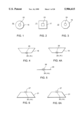
- FIG. 1 is a top schematic view, omitting certain details described below, of a first embodiment of an antenna structure in accordance with the invention
- FIG. 2 is a top schematic view, omitting certain details described below, of a second embodiment of an antenna structure in accordance with the invention
- FIG. 3 is a top schematic view, omitting certain details described below, of a third embodiment of an antenna structure in accordance with the invention.
- FIGS. 4, 5 and 6 are side sectional schematic views, omitting certain details described below, respectively showing embodiments of concave up, planar, and concave down ground planes, each of which can have any of the shapes in plan view shown in FIGS. 1-3;
- FIG. 4A and 6A are views similar to FIGS. 4 and 6, respectively, showing other embodiments of the invention.
- FIGS. 7-10 are top views, omitting certain details described below, of respective embodiments of the invention wherein the radiating element and the ground plane have dissimilar shapes;
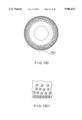
- FIG. 11 is a top view showing in more detail a preferred embodiment of an antenna structure in accordance with the invention.
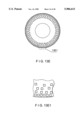
- FIG. 12A is a view similar to FIG. 11 showing a portion enlarged to reveal a first type of cutout employed in accordance with the invention;
- FIG. 12A1 shows a portion of FIG. 12A on an enlarged scale
- FIGS. 12B and 12B1 are views similar to FIGS. 12A and 12A1, respectively but showing another type of cutout;
- FIGS. 12C and 12C1 are views similar to FIGS. 12A and 12A1, respectively but showing another type of cutout;
- FIGS. 12D and 12E and 12E1 are views similar to FIGS. 12A and 12A1, respectively but showing other types of cutouts;
- FIGS. 12D-1 to 12D-4 show modifications of the structure of FIG. 12D;
- FIGS. 13A to 13F show modifications of the structure of FIG. 12E;
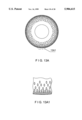
- FIG. 14 is a graph showing the resistive profile of a ground plane employed in a preferred embodiment of the invention.
- FIGS. 15-18 are plots illustrating an important advantage of the invention.
- FIGS. 1-3 are top schematic views of antenna structures 10-12 constructed in accordance with the invention
- FIGS. 4, 4A, 5, 6 and 6A respectively show other features that can be incorporated in antenna structures in accordance with the invention.
- the antenna structure 10 comprises a ground plane 16 and a radiating element 22. Both the ground plane 16 and the radiating element 22 are circular. In FIG. 2 both (17, 23) are square; and in FIG. 3 both (18, 24) are octagonal.
- the ground planes 16, 17, 18 are illustrated as planar, but, as FIGS. 4, 4A, 6 and 6A illustrate, they need not be.
- the ground plane 19 is frustoconical and concave up
- in FIG. 6 the ground plane 21 is frustoconical and concave down.
- the ground planes are frustopyramidal and concave respectively up and down.
- FIG. 4A and 6A the ground planes are frustopyramidal and concave respectively up and down.
- the ground plane 20 is planar.
- the ground plane can have any of the shapes illustrated in FIGS. 1-3--circular, square or octagonal--combined with any of the shapes illustrated in FIGS. 4, 4A, 5, 6 and 6A.
- Other shapes both in plan view and in side section are also within the scope of the invention, as those skilled in the art will readily understand.
- FIGS. 7-10 show embodiments of the invention wherein the radiating element and the ground plane have dissimilar shapes: respectively round/square in FIG. 7, square/round in FIG. 8, round/octagonal in FIG. 9, and square/octagonal in FIG. 10. Other combinations of dissimilar shapes will readily occur to those skilled in the art in light of this disclosure.
- each spiral arm is fed by a power divider with an integral phase shifter to give each arm a successive 90-degree shift (to 0°, 90°, 180°, and 270°).
- a conductive portion which can be formed of a metal such as aluminum or of a nonconductive material such as a woven cloth or a plastic disk impregnated with, or having a coating of, aluminum, another metal, or another conductive material.
- Aluminum plates 28-30 are illustrated in FIGS. 4, 4A, 5, 6 and 6A (an aluminum plate is of course highly conductive).
- the aluminum plate has an outer diameter of, say, 5 inches (about 13 cm).
- the ground plane has an outer diameter of, say, 13 inches (about 33 cm).
- Sheet resistivity is measured in ohms per square.
- the current that flows is independent of the size of the square. For example, if the size of the square is doubled, the current must flow through double the length of the material, thereby doubling the resistance offered by each longitudinal segment of the square (i.e., each segment extending from the high-potential side of the square to the low-potential side).
- doubling the size of the square in effect adds a second resistor in parallel to the first and identical to it, thereby reducing the resistance by half.
- the ground plane in the preferred embodiment of the invention has a sheet resistivity substantially in the range of 0 to 3 ohms per square measured from dead center to a position adjacent the periphery of the radiating element and a resistivity of substantially 500-800 ohms per square measured at the periphery of the ground plane.
- the resistivity of the peripheral region thus exceeds that in the central region by several orders of magnitude, whereby the ground plane, through physically small, simulates an infinite ground plane.
- the sheet resistivity of free space is 377 ohms per square.
- the sheet resistivity of the ground plane at the outer periphery is thus much higher than that of free space.
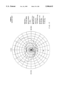
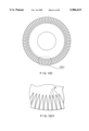
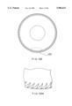
- FIG. 11 shows an antenna structure 40 in accordance with the invention.
- a radiating element as illustrated in any of the preceding figures is employed.
- FIG. 11 shows a ground plane 42 for the radiating element.
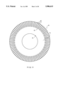
- the ground plane has a central region 44 closely spaced apart from the radiating element and a peripheral region 46 extending away from the central region 44.
- the peripheral 46 is formed with at least one cutout 48 having an area that increases as radial distance from the central region 44 increases.
- the peripheral region 46 can be formed with a plurality of cutouts.
- Each cutout can be, for example, U-shaped, as shown in FIG. 12A and FIG. 12A1, or V-shaped, as shown in FIG. 12B and FIG. 12B1.
- Each U or V has a narrow end 50 or 52 near the central region 44 and a wide end 54 or 56 remote from the central region.
- the cutouts can have edges 58 that form an exponential curve.
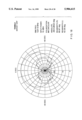
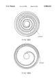
- FIG. 12D and FIG. 12D4 shows, the cutouts can also be spiral-shaped.
- the cutout may describe as spiral about a central point, the spiral subtending an arc of at least 360° as measured from the central point or an arc of a multiple of 360° (FIG. 12D-1).
- the spiral in that case can form loops that are closer together as radial distance from the central region increases (FIG. 12D-2) or that become wider (FIG. 12D-3).
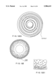
- the peripheral region can formed with a plurality of cutouts, each cutout being a closed figure and the cutouts collectively having an area that increases as radial distance from the central region increases.
- the cutouts can be elliptical (FIG. 13A and FIG. 13A1), circular (FIG. 13B and FIG. 13B1), polygonal (FIG. 13C and FIG. 13C1), rectangular (FIG. 13D and FIG. 13D1), square (FIG. 13E and FIG. 13E1), or have any other closed shape.
- the peripheral region prefferably has a first plurality of cutouts each extending from the central region to the periphery and a second plurality of cutouts interspersed with the first plurality of cutouts and each extending from a position spaced apart from the central region to the periphery (FIG. 13F).
- resistivity measured from the inner edge to the outer edge has a resistive profile varying in accordance with the following formula:
- the conductive center of the ground plane is 4.97 inches square (about 12.6 cm square) and approximately covers the "hole" in the ground plane. From another standpoint, the ground plane extends radially out approximately from the edges of the conductive center of the ground plane.
- a patch is employed as the radiating element, its dimensions will depend on the dielectric. If air is the dielectric, the patch can be, say, 2 inches (about 5 cm) on a side. If a material of higher dielectric constant is employed, the size of the patch can be reduced to, say, 1.5 inches (about 3.8 cm) on a side.
- FIG. 14 shows the resistivity profile of the ground plane for the preferred embodiment of the invention.
- equation (1) consider for example a position 2.4 inches measured radially outward from the inner edge of the ground plane.
- the resistivity is calculated from equation (1) as follows:
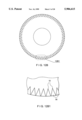
- FIGS. 15 and 16 show the antenna pattern without a ground plane (at the two GPS frequencies).
- FIGS. 17 and 18 show the antenna pattern in accordance with the invention at the two GPS frequencies. The important thing to notice is that the back lobes (the area under the curves on the bottom half of the plots) are reduced in FIGS. 17 and 18.
- the two lines on each plot represent the received signal strength of a right hand circular polarized (RHCP) signal and a left hand (LHCP) signal, corresponding to a GPS signal and a reflected signal.
- RHCP right hand circular polarized
- LHCP left hand
- the antenna structure described above reduces multipath signals caused by reflection from the earth.
- the ground plane though physically small, simulates an infinite ground plane because of its varying sheet resistivity. Signals reflected from the ground and impinging on the underside of the antenna structure are absorbed by the ground plane and dissipated as heat; they do not interact substantially with the antenna proper.
- the antenna is particularly adapted for use in a GPS receiver that receives and processes signals from navigation satellites. Because of its light weight, it is suitable for hand-held units of the type used by surveyors.
Abstract
Description
R=3+4.9881((exp 1.258×)-1) (1)
Claims (38)
Priority Applications (1)
| Application Number | Priority Date | Filing Date | Title |
|---|---|---|---|
| US08/934,146 US5986615A (en) | 1997-09-19 | 1997-09-19 | Antenna with ground plane having cutouts |
Applications Claiming Priority (1)
| Application Number | Priority Date | Filing Date | Title |
|---|---|---|---|
| US08/934,146 US5986615A (en) | 1997-09-19 | 1997-09-19 | Antenna with ground plane having cutouts |
Publications (1)
| Publication Number | Publication Date |
|---|---|
| US5986615A true US5986615A (en) | 1999-11-16 |
Family
ID=25465039
Family Applications (1)
| Application Number | Title | Priority Date | Filing Date |
|---|---|---|---|
| US08/934,146 Expired - Lifetime US5986615A (en) | 1997-09-19 | 1997-09-19 | Antenna with ground plane having cutouts |
Country Status (1)
| Country | Link |
|---|---|
| US (1) | US5986615A (en) |
Cited By (15)
| Publication number | Priority date | Publication date | Assignee | Title |
|---|---|---|---|---|
| US6100855A (en) * | 1999-02-26 | 2000-08-08 | Marconi Aerospace Defence Systems, Inc. | Ground plane for GPS patch antenna |
| US6255995B1 (en) * | 1998-12-24 | 2001-07-03 | International Business Machines Corporation | Patch antenna and electronic equipment using the same |
| US6836247B2 (en) | 2002-09-19 | 2004-12-28 | Topcon Gps Llc | Antenna structures for reducing the effects of multipath radio signals |
| EP1564841A1 (en) * | 2002-10-23 | 2005-08-17 | Sony Corporation | Unbalanced antenna |
| US7148850B2 (en) | 2000-01-19 | 2006-12-12 | Fractus, S.A. | Space-filling miniature antennas |
| WO2008132495A1 (en) * | 2007-04-27 | 2008-11-06 | Antenova Limited | Antenna device with crenellated groundplane |
| US20090096704A1 (en) * | 2007-09-17 | 2009-04-16 | Physical Sciences, Inc. | Non-Cutoff Frequency Selective Surface Ground Plane Antenna Assembly |
| US8009111B2 (en) | 1999-09-20 | 2011-08-30 | Fractus, S.A. | Multilevel antennae |
| US8738103B2 (en) | 2006-07-18 | 2014-05-27 | Fractus, S.A. | Multiple-body-configuration multimedia and smartphone multifunction wireless devices |
| US20150123868A1 (en) * | 2013-11-06 | 2015-05-07 | Motorola Solutions, Inc. | Compact, multi-port, mimo antenna with high port isolation and low pattern correlation and method of making same |
| US9048546B2 (en) | 2010-01-22 | 2015-06-02 | Topcon Positioning Systems, Inc. | Flat semi-transparent ground plane for reducing multipath reception and antenna system |
| US20150263434A1 (en) | 2013-03-15 | 2015-09-17 | SeeScan, Inc. | Dual antenna systems with variable polarization |
| US9917369B2 (en) | 2015-09-23 | 2018-03-13 | Topcon Positioning Systems, Inc. | Compact broadband antenna system with enhanced multipath rejection |
| US10158178B2 (en) | 2013-11-06 | 2018-12-18 | Symbol Technologies, Llc | Low profile, antenna array for an RFID reader and method of making same |
| US10608348B2 (en) | 2012-03-31 | 2020-03-31 | SeeScan, Inc. | Dual antenna systems with variable polarization |
Citations (13)
| Publication number | Priority date | Publication date | Assignee | Title |
|---|---|---|---|---|
| GB2057773A (en) * | 1979-09-06 | 1981-04-01 | Marconi Co Ltd | Aerial systems |
| US4529987A (en) * | 1982-05-13 | 1985-07-16 | Her Majesty The Queen In Right Of Canada, As Represented By The Minister Of National Defence Of Her Majesty's Canadian Government | Broadband microstrip antennas with varactor diodes |
| DE3738513A1 (en) * | 1987-11-13 | 1989-06-01 | Dornier System Gmbh | MICROSTRIP LADDER AERIAL |
| EP0318873A1 (en) * | 1987-11-28 | 1989-06-07 | Toppan Printing Co., Ltd. | Electromagnetic wave absorbing element |
| US4927251A (en) * | 1988-06-13 | 1990-05-22 | Schoen Neil C | Single pass phase conjugate aberration correcting imaging telescope |
| US4965603A (en) * | 1989-08-01 | 1990-10-23 | Rockwell International Corporation | Optical beamforming network for controlling an RF phased array |
| EP0394960A1 (en) * | 1989-04-26 | 1990-10-31 | Kokusai Denshin Denwa Co., Ltd | A microstrip antenna |
| US5132623A (en) * | 1990-11-20 | 1992-07-21 | Chevron Research And Technology Company | Method and apparatus for broadband measurement of dielectric properties |
| US5170175A (en) * | 1991-08-23 | 1992-12-08 | Motorola, Inc. | Thin film resistive loading for antennas |
| US5204685A (en) * | 1992-07-01 | 1993-04-20 | The United States Of America As Represented By The Secretary Of The Air Force | ARC range test facility |
| US5248980A (en) * | 1991-04-05 | 1993-09-28 | Alcatel Espace | Spacecraft payload architecture |
| DE4326117A1 (en) * | 1993-08-04 | 1995-02-09 | Philips Patentverwaltung | Two-way radio with an antenna |
| US5592174A (en) * | 1995-01-26 | 1997-01-07 | Lockheed Martin Corporation | GPS multi-path signal reception |
-
1997
- 1997-09-19 US US08/934,146 patent/US5986615A/en not_active Expired - Lifetime
Patent Citations (14)
| Publication number | Priority date | Publication date | Assignee | Title |
|---|---|---|---|---|
| GB2057773A (en) * | 1979-09-06 | 1981-04-01 | Marconi Co Ltd | Aerial systems |
| US4529987A (en) * | 1982-05-13 | 1985-07-16 | Her Majesty The Queen In Right Of Canada, As Represented By The Minister Of National Defence Of Her Majesty's Canadian Government | Broadband microstrip antennas with varactor diodes |
| DE3738513A1 (en) * | 1987-11-13 | 1989-06-01 | Dornier System Gmbh | MICROSTRIP LADDER AERIAL |
| US5061938A (en) * | 1987-11-13 | 1991-10-29 | Dornier System Gmbh | Microstrip antenna |
| EP0318873A1 (en) * | 1987-11-28 | 1989-06-07 | Toppan Printing Co., Ltd. | Electromagnetic wave absorbing element |
| US4927251A (en) * | 1988-06-13 | 1990-05-22 | Schoen Neil C | Single pass phase conjugate aberration correcting imaging telescope |
| EP0394960A1 (en) * | 1989-04-26 | 1990-10-31 | Kokusai Denshin Denwa Co., Ltd | A microstrip antenna |
| US4965603A (en) * | 1989-08-01 | 1990-10-23 | Rockwell International Corporation | Optical beamforming network for controlling an RF phased array |
| US5132623A (en) * | 1990-11-20 | 1992-07-21 | Chevron Research And Technology Company | Method and apparatus for broadband measurement of dielectric properties |
| US5248980A (en) * | 1991-04-05 | 1993-09-28 | Alcatel Espace | Spacecraft payload architecture |
| US5170175A (en) * | 1991-08-23 | 1992-12-08 | Motorola, Inc. | Thin film resistive loading for antennas |
| US5204685A (en) * | 1992-07-01 | 1993-04-20 | The United States Of America As Represented By The Secretary Of The Air Force | ARC range test facility |
| DE4326117A1 (en) * | 1993-08-04 | 1995-02-09 | Philips Patentverwaltung | Two-way radio with an antenna |
| US5592174A (en) * | 1995-01-26 | 1997-01-07 | Lockheed Martin Corporation | GPS multi-path signal reception |
Non-Patent Citations (4)
| Title |
|---|
| Analysis and Treatment of Edge Effects on the Radiation Pattern of a Microstrip Patch Antenna, 0 7803 2719 5/95/S4. 1995 IEEE, Michael F. Otero et al. * |
| Analysis and Treatment of Edge Effects on the Radiation Pattern of a Microstrip Patch Antenna, 0-7803-2719-5/95/S4. 1995 IEEE, Michael F. Otero et al. |
| Synsthesis of Tapered Resistive Ground Plane for a Microstrip Antenna, 0 7803 2719 5/95/S4. 1995 IEEE, R.G. Rojas et al. * |
| Synsthesis of Tapered Resistive Ground Plane for a Microstrip Antenna, 0-7803-2719-5/95/S4. 1995 IEEE, R.G. Rojas et al. |
Cited By (51)
| Publication number | Priority date | Publication date | Assignee | Title |
|---|---|---|---|---|
| US6255995B1 (en) * | 1998-12-24 | 2001-07-03 | International Business Machines Corporation | Patch antenna and electronic equipment using the same |
| US6100855A (en) * | 1999-02-26 | 2000-08-08 | Marconi Aerospace Defence Systems, Inc. | Ground plane for GPS patch antenna |
| US9054421B2 (en) | 1999-09-20 | 2015-06-09 | Fractus, S.A. | Multilevel antennae |
| US9761934B2 (en) | 1999-09-20 | 2017-09-12 | Fractus, S.A. | Multilevel antennae |
| US9362617B2 (en) | 1999-09-20 | 2016-06-07 | Fractus, S.A. | Multilevel antennae |
| US9240632B2 (en) | 1999-09-20 | 2016-01-19 | Fractus, S.A. | Multilevel antennae |
| US8009111B2 (en) | 1999-09-20 | 2011-08-30 | Fractus, S.A. | Multilevel antennae |
| US9000985B2 (en) | 1999-09-20 | 2015-04-07 | Fractus, S.A. | Multilevel antennae |
| US8976069B2 (en) | 1999-09-20 | 2015-03-10 | Fractus, S.A. | Multilevel antennae |
| US8941541B2 (en) | 1999-09-20 | 2015-01-27 | Fractus, S.A. | Multilevel antennae |
| US10056682B2 (en) | 1999-09-20 | 2018-08-21 | Fractus, S.A. | Multilevel antennae |
| US8330659B2 (en) | 1999-09-20 | 2012-12-11 | Fractus, S.A. | Multilevel antennae |
| US8154463B2 (en) | 1999-09-20 | 2012-04-10 | Fractus, S.A. | Multilevel antennae |
| US8154462B2 (en) | 1999-09-20 | 2012-04-10 | Fractus, S.A. | Multilevel antennae |
| US8558741B2 (en) | 2000-01-19 | 2013-10-15 | Fractus, S.A. | Space-filling miniature antennas |
| US7202822B2 (en) | 2000-01-19 | 2007-04-10 | Fractus, S.A. | Space-filling miniature antennas |
| US7554490B2 (en) | 2000-01-19 | 2009-06-30 | Fractus, S.A. | Space-filling miniature antennas |
| US10355346B2 (en) | 2000-01-19 | 2019-07-16 | Fractus, S.A. | Space-filling miniature antennas |
| US8207893B2 (en) | 2000-01-19 | 2012-06-26 | Fractus, S.A. | Space-filling miniature antennas |
| US8212726B2 (en) | 2000-01-19 | 2012-07-03 | Fractus, Sa | Space-filling miniature antennas |
| US9331382B2 (en) | 2000-01-19 | 2016-05-03 | Fractus, S.A. | Space-filling miniature antennas |
| US7148850B2 (en) | 2000-01-19 | 2006-12-12 | Fractus, S.A. | Space-filling miniature antennas |
| US8471772B2 (en) | 2000-01-19 | 2013-06-25 | Fractus, S.A. | Space-filling miniature antennas |
| US7164386B2 (en) | 2000-01-19 | 2007-01-16 | Fractus, S.A. | Space-filling miniature antennas |
| US8610627B2 (en) | 2000-01-19 | 2013-12-17 | Fractus, S.A. | Space-filling miniature antennas |
| US6836247B2 (en) | 2002-09-19 | 2004-12-28 | Topcon Gps Llc | Antenna structures for reducing the effects of multipath radio signals |
| US20070176828A1 (en) * | 2002-10-23 | 2007-08-02 | Sony Corporation | Unbalanced antenna |
| US20060214869A1 (en) * | 2002-10-23 | 2006-09-28 | Sony Corporation | Unbalanced antenna |
| US7180466B2 (en) | 2002-10-23 | 2007-02-20 | Sony Corporation | Unbalanced antenna |
| US7515114B2 (en) | 2002-10-23 | 2009-04-07 | Sony Corporation | Unbalanced antenna |
| EP1564841A1 (en) * | 2002-10-23 | 2005-08-17 | Sony Corporation | Unbalanced antenna |
| EP1564841A4 (en) * | 2002-10-23 | 2005-12-21 | Sony Corp | Unbalanced antenna |
| US11031677B2 (en) | 2006-07-18 | 2021-06-08 | Fractus, S.A. | Multiple-body-configuration multimedia and smartphone multifunction wireless devices |
| US9099773B2 (en) | 2006-07-18 | 2015-08-04 | Fractus, S.A. | Multiple-body-configuration multimedia and smartphone multifunction wireless devices |
| US11349200B2 (en) | 2006-07-18 | 2022-05-31 | Fractus, S.A. | Multiple-body-configuration multimedia and smartphone multifunction wireless devices |
| US11735810B2 (en) | 2006-07-18 | 2023-08-22 | Fractus, S.A. | Multiple-body-configuration multimedia and smartphone multifunction wireless devices |
| US8738103B2 (en) | 2006-07-18 | 2014-05-27 | Fractus, S.A. | Multiple-body-configuration multimedia and smartphone multifunction wireless devices |
| US9899727B2 (en) | 2006-07-18 | 2018-02-20 | Fractus, S.A. | Multiple-body-configuration multimedia and smartphone multifunction wireless devices |
| US10644380B2 (en) | 2006-07-18 | 2020-05-05 | Fractus, S.A. | Multiple-body-configuration multimedia and smartphone multifunction wireless devices |
| WO2008132495A1 (en) * | 2007-04-27 | 2008-11-06 | Antenova Limited | Antenna device with crenellated groundplane |
| US8451190B2 (en) | 2007-09-17 | 2013-05-28 | Physical Sciences, Inc. | Non-cutoff frequency selective surface ground plane antenna assembly |
| US8004474B2 (en) | 2007-09-17 | 2011-08-23 | Physical Sciences, Inc. | Non-cutoff frequency selective surface ground plane antenna assembly |
| US20090096704A1 (en) * | 2007-09-17 | 2009-04-16 | Physical Sciences, Inc. | Non-Cutoff Frequency Selective Surface Ground Plane Antenna Assembly |
| US9048546B2 (en) | 2010-01-22 | 2015-06-02 | Topcon Positioning Systems, Inc. | Flat semi-transparent ground plane for reducing multipath reception and antenna system |
| US10608348B2 (en) | 2012-03-31 | 2020-03-31 | SeeScan, Inc. | Dual antenna systems with variable polarization |
| US10490908B2 (en) | 2013-03-15 | 2019-11-26 | SeeScan, Inc. | Dual antenna systems with variable polarization |
| US20150263434A1 (en) | 2013-03-15 | 2015-09-17 | SeeScan, Inc. | Dual antenna systems with variable polarization |
| US10158178B2 (en) | 2013-11-06 | 2018-12-18 | Symbol Technologies, Llc | Low profile, antenna array for an RFID reader and method of making same |
| US9847571B2 (en) * | 2013-11-06 | 2017-12-19 | Symbol Technologies, Llc | Compact, multi-port, MIMO antenna with high port isolation and low pattern correlation and method of making same |
| US20150123868A1 (en) * | 2013-11-06 | 2015-05-07 | Motorola Solutions, Inc. | Compact, multi-port, mimo antenna with high port isolation and low pattern correlation and method of making same |
| US9917369B2 (en) | 2015-09-23 | 2018-03-13 | Topcon Positioning Systems, Inc. | Compact broadband antenna system with enhanced multipath rejection |
Similar Documents
| Publication | Publication Date | Title |
|---|---|---|
| US5694136A (en) | Antenna with R-card ground plane | |
| US5986615A (en) | Antenna with ground plane having cutouts | |
| US6014114A (en) | Antenna with stepped ground plane | |
| US6366254B1 (en) | Planar antenna with switched beam diversity for interference reduction in a mobile environment | |
| US6518931B1 (en) | Vivaldi cloverleaf antenna | |
| US6121931A (en) | Planar dual-frequency array antenna | |
| US5831582A (en) | Multiple beam antenna system for simultaneously receiving multiple satellite signals | |
| Sumantyo et al. | Dual-band circularly polarized equilateral triangular-patch array antenna for mobile satellite communications | |
| US7498989B1 (en) | Stacked-disk antenna element with wings, and array thereof | |
| US6100855A (en) | Ground plane for GPS patch antenna | |
| US20170187109A1 (en) | Final fabrication and calibration steps for hierarchically elaborated phased-array antenna and subarray manufacturing process | |
| US20070241984A1 (en) | Vertically polarized traveling wave antenna apparatus and method | |
| NO318278B1 (en) | Wide-angle antenna with circular polarization | |
| US20090027294A1 (en) | Omni-directional antenna for mobile satellite broadcasting applications | |
| US4081803A (en) | Multioctave turnstile antenna for direction finding and polarization determination | |
| EP3591760A1 (en) | Supplemental device for an antenna system | |
| SE511907C2 (en) | Integrated communication device | |
| US20030164805A1 (en) | Pentagonal helical antenna array | |
| US7170449B2 (en) | Antenna system for georadar | |
| US5945950A (en) | Stacked microstrip antenna for wireless communication | |
| US20120019425A1 (en) | Antenna For Increasing Beamwidth Of An Antenna Radiation Pattern | |
| EP0825676B1 (en) | Complementary bowtie antenna | |
| CA2064295C (en) | Microwave polarizing lens structure | |
| US10823812B2 (en) | eLORAN receiver with ferromagnetic body and related antennas and methods | |
| Jang et al. | Design of a 16‐element array antenna with a planar L‐shaped probe for a direction of arrival estimation of the unidentified broadband signal |
Legal Events
| Date | Code | Title | Description |
|---|---|---|---|
| AS | Assignment |
Owner name: TRIMBLE NAVIGATION LIMITED, CALIFORNIA Free format text: ASSIGNMENT OF ASSIGNORS INTEREST;ASSIGNORS:WESTFALL, BRIAN G.;STEPHENSON, KEVIN B.;REEL/FRAME:008822/0783 Effective date: 19970917 |
|
| STCF | Information on status: patent grant |
Free format text: PATENTED CASE |
|
| AS | Assignment |
Owner name: ABN AMRO BANK N.V., AS AGENT, ILLINOIS Free format text: SECURITY AGREEMENT;ASSIGNOR:TRIMBLE NAVIGATION LIMITED;REEL/FRAME:010996/0643 Effective date: 20000714 |
|
| FEPP | Fee payment procedure |
Free format text: PAYOR NUMBER ASSIGNED (ORIGINAL EVENT CODE: ASPN); ENTITY STATUS OF PATENT OWNER: LARGE ENTITY |
|
| FPAY | Fee payment |
Year of fee payment: 4 |
|
| AS | Assignment |
Owner name: TRIMBLE NAVIGATION LIMITED, CALIFORNIA Free format text: RELEASE OF SECURITY INTEREST;ASSIGNOR:ABN AMRO BANK N.V.;REEL/FRAME:016345/0177 Effective date: 20050620 |
|
| FPAY | Fee payment |
Year of fee payment: 8 |
|
| SULP | Surcharge for late payment |
Year of fee payment: 7 |
|
| FPAY | Fee payment |
Year of fee payment: 12 |