US5995285A - Multilevel optical diffraction device with antireflection film and exposure apparatus - Google Patents
Multilevel optical diffraction device with antireflection film and exposure apparatus Download PDFInfo
- Publication number
- US5995285A US5995285A US08/889,859 US88985997A US5995285A US 5995285 A US5995285 A US 5995285A US 88985997 A US88985997 A US 88985997A US 5995285 A US5995285 A US 5995285A
- Authority
- US
- United States
- Prior art keywords
- diffraction device
- optical diffraction
- antireflection film
- shaped elements
- substrate
- Prior art date
- Legal status (The legal status is an assumption and is not a legal conclusion. Google has not performed a legal analysis and makes no representation as to the accuracy of the status listed.)
- Expired - Lifetime
Links
Images


Classifications
-
- G—PHYSICS
- G03—PHOTOGRAPHY; CINEMATOGRAPHY; ANALOGOUS TECHNIQUES USING WAVES OTHER THAN OPTICAL WAVES; ELECTROGRAPHY; HOLOGRAPHY
- G03F—PHOTOMECHANICAL PRODUCTION OF TEXTURED OR PATTERNED SURFACES, e.g. FOR PRINTING, FOR PROCESSING OF SEMICONDUCTOR DEVICES; MATERIALS THEREFOR; ORIGINALS THEREFOR; APPARATUS SPECIALLY ADAPTED THEREFOR
- G03F7/00—Photomechanical, e.g. photolithographic, production of textured or patterned surfaces, e.g. printing surfaces; Materials therefor, e.g. comprising photoresists; Apparatus specially adapted therefor
- G03F7/70—Microphotolithographic exposure; Apparatus therefor
- G03F7/70058—Mask illumination systems
-
- G—PHYSICS
- G02—OPTICS
- G02B—OPTICAL ELEMENTS, SYSTEMS OR APPARATUS
- G02B5/00—Optical elements other than lenses
- G02B5/18—Diffraction gratings
- G02B5/1847—Manufacturing methods
- G02B5/1857—Manufacturing methods using exposure or etching means, e.g. holography, photolithography, exposure to electron or ion beams
-
- G—PHYSICS
- G02—OPTICS
- G02B—OPTICAL ELEMENTS, SYSTEMS OR APPARATUS
- G02B5/00—Optical elements other than lenses
- G02B5/18—Diffraction gratings
- G02B5/1876—Diffractive Fresnel lenses; Zone plates; Kinoforms
-
- G—PHYSICS
- G03—PHOTOGRAPHY; CINEMATOGRAPHY; ANALOGOUS TECHNIQUES USING WAVES OTHER THAN OPTICAL WAVES; ELECTROGRAPHY; HOLOGRAPHY
- G03F—PHOTOMECHANICAL PRODUCTION OF TEXTURED OR PATTERNED SURFACES, e.g. FOR PRINTING, FOR PROCESSING OF SEMICONDUCTOR DEVICES; MATERIALS THEREFOR; ORIGINALS THEREFOR; APPARATUS SPECIALLY ADAPTED THEREFOR
- G03F7/00—Photomechanical, e.g. photolithographic, production of textured or patterned surfaces, e.g. printing surfaces; Materials therefor, e.g. comprising photoresists; Apparatus specially adapted therefor
- G03F7/70—Microphotolithographic exposure; Apparatus therefor
- G03F7/70216—Mask projection systems
- G03F7/70241—Optical aspects of refractive lens systems, i.e. comprising only refractive elements
Definitions
- the present invention relates to an optical diffraction device, and more particularly to a binary-type optical diffraction device.
- the invention also relates to an optical system including a binary-type optical diffraction device and to an optical apparatus such as an exposure apparatus, including such an optical system.
- a binary device is regarded in the art as an important possible technique to realize a high-accuracy optical diffraction device.
- the binary device is a technique to produce an optical diffraction device having a step structure in cross section such as that shown in FIG. 1B, which is an approximation of the blazed cross-sectional structure of an optical diffraction device such as that shown in FIG. 1A.
- the optical device shown in FIGS. 1A and 1B is a diffraction-type Fresnel lens, which is also called a kinoform.
- a diffraction grating having a fine structure is formed on a transparent substrate 100 or 101. If the structure of the diffraction device is approximated by a step structure, the diffraction device can be easily produced with high precision using the semiconductor process technology which is widely used to produce an LSI or the like.
- FIGS. 2A-H illustrates the process of producing a 4-step optical diffraction device (binary device) using the semiconductor process technology.
- reference numeral 110 denotes a transparent substrate on which a diffraction grating is formed, 111 a resist coated on the substrate 110, and 112 a mask used to form a grating pattern.
- the resist 111 is exposed via the mask 112 to exposure light 113 so as to form a latent image corresponding to the mask pattern.
- the resist is developed so that the portions exposed to light (latent image) are removed (herein the resist is assumed to be of the positive type).
- the resist is assumed to be of the positive type.
- the substrate 110 is etched to a predetermined depth by means of the reactive ion etching technique. Then, the remaining resist is removed.
- a 2-step structure is obtained as shown in FIG. 2D.
- another resist 114 is coated on the surface of the substrate, and the resist 114 is exposed via a mask 114 having a grating pattern with a pitch half that of the pattern formed on the mask 112.
- the resist 114 is developed so that exposed portions of the resist are removed as in the previous development process, and the substrate 110 is etched using the remaining resist as a mask. After that, the remaining resist is removed.
- a 4-step structure is obtained as shown in FIG. 2H.
- the above processing steps are repeated using a mask having a pattern with a pitch half that of the pattern formed on the mask 115.
- the number of steps in the structure is limited to 2 n (n: integer)
- a desired step structure is formed by etching a substrate.
- FIG. 3 illustrates, in an enlarged fashion, a part of an optical diffraction device.
- the step structure will be discussed in further detail below.
- the refractive index of the substrate 120 is n s and the refractive index of the medium 121 on which light is incident is n i .
- the broken line 122 represents the ideal structure of the device while the solid line 123 represents the structure which approximates the ideal structure by steps.
- the height D of the ideal structure 122 should be
- the height of each step is given by the above equation.
- the height of each step may also be determined in another way.
- k may have an arbitrary value within the range 0 ⁇ k ⁇ 1.
- the surface of an optical device is generally covered with an antireflection film for suppressing the reflection of light at the surface.
- an antireflection film for suppressing the reflection of light at the surface.
- a dioptric lens since the surface is smooth, it is easy to form an antireflection film on the surface.
- binary devices a technique of forming an antireflection film on the device surface is disclosed in "Antireflection-coated diffractive optical devices fabricated by thin-film deposition", E. Pawlowski and B. Kuhlow, Opt. Eng. 33(11), 3537-3546 (1994). In this technique, as shown in FIG.
- a material 131 for forming an antireflection film is deposited from above at right angle onto the surface of a substrate 130 by means of ion beam sputtering thereby forming a thin film 132 on the step-structured surface of the substrate 130.
- FIG. 5 illustrates a multilayer antireflection film formed on the fine step-structured surface using the sputtering technique.
- the antireflection film 143 formed on substrate 141 using the conventional technique has ununiformity in thickness due to the steps, which causes a reduction in antireflection effect.
- an optical diffraction device including: a plurality of step-shaped elements; and an antireflection film having a flat surface, the plurality of step-shaped elements being entirely covered with the antireflection film.
- the antireflection film consists of a single transparent layer.
- the antireflection film may also consist of two transparent layers having different refractive indices wherein one layer is disposed on the other layer.
- an optical diffraction device including: a plurality of step-shaped elements; and a reflection enhancement film having a flat surface, the plurality of step-shaped elements being entirely covered with the reflection enhancement film.
- the reflection enhancement film consists of a single transparent layer.
- the reflection enhancement film may also consist of two transparent layers having different refractive indices wherein one layer is disposed on the other layer.
- an optical diffraction device including a plurality of step-shaped elements, wherein the plurality of step-shaped elements are formed so that interference among light rays reflected from the plurality of step-shaped elements causes the overall intensity of the reflected light rays to become substantially zero.
- Various optical systems and apparatuses using the above optical diffraction device, and a production method thereof, are also disclosed.
- the plurality of step-shaped elements are formed so that the following conditions are satisfied:
- ⁇ is the wavelength of the reflected light rays
- n s is the refractive index of each step-shaped element
- n i is the refractive index of a medium occupying the space in contact with the incidence side of the plurality of step-shaped elements
- L is the number of the step-shaped elements
- h is the height of each step-shaped element
- p is an integer equal to or greater than 2.
- the plurality of step-shaped elements are preferably formed so that the following conditions are satisfied:
- ⁇ is the wavelength of the reflected light rays
- n s is the refractive index of each step-shaped element
- n j is the refractive index of a medium occupying the space in contact with the light emerging side of the plurality of step-shaped elements
- L is the number of the step-shaped elements
- h is the height of each step-shaped element
- p is an integer equal to or greater than 2.
- FIGS. 1A and 1B are schematic diagrams illustrating cross sections of a conventional diffraction device and a binary-type diffraction device
- FIGS. 2A through 2H are schematic diagrams illustrating the processing steps of producing a binary-type diffraction device
- FIG. 3 is a schematic diagram illustrating the method of determining the height of steps of the binary device
- FIG. 4 is a schematic diagram illustrating a conventional method of producing an antireflection film
- FIG. 5 is a schematic diagram illustrating the structure of a conventional antireflection film
- FIG. 6 is a cross-sectional view of a first embodiment of a binary-type optical diffraction device according to the invention.
- FIG. 7 is a schematic diagram illustrating the function of a single-layer antireflection film
- FIG. 8 is an enlarged cross-sectional view illustrating a part of a binary-type optical device according to a first embodiment of the invention.
- FIGS. 9A through 9C are schematic diagrams illustrating a method of producing an antireflection film
- FIG. 10 is a schematic diagram illustrating the function of a two-layer antireflection film
- FIG. 11 is a cross-sectional view of a second embodiment of a binary-type optical diffraction device according to the invention.
- FIG. 12 is a cross-sectional view of a third embodiment of a binary-type optical diffraction device according to the invention.
- FIG. 13 is a schematic diagram illustrating a condition in which reflected light is eliminated
- FIG. 14 is a schematic diagram illustrating another condition in which reflected light is eliminated.
- FIG. 15 is a schematic diagram illustrating still another condition in which reflected light is eliminated.
- FIG. 16 is a schematic diagram illustrating another condition in which reflected light is eliminated.
- FIG. 17 is a schematic diagram illustrating still another condition in which reflected light is eliminated.
- FIG. 18 is a schematic diagram illustrating a combination of an antireflection film and a binary-type optical diffraction device
- FIG. 19 is a schematic diagram illustrating a projecting optical system
- FIG. 20 is a schematic diagram illustrating a projection exposure apparatus
- FIG. 21 is a flowchart illustrating the processing steps of producing a semiconductor device.
- FIG. 22 is a flowchart illustrating the details of the wafer process shown in FIG. 21.
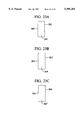
- FIGS. 23A through 23C are schematic diagrams each illustrating a transparent substrate with step-shaped elements on at least one surface.
- FIG. 6 illustrates a binary-type optical device (binary device) having an antireflection film formed over a plurality of steps located side by side on the surface of the device.
- This optical device is a Fresnel lens similar to that shown in FIG. 1.
- reference numeral 1 denotes a transparent substrate (with a refractive index of n s ) on the surface of which a plurality of steps are formed.
- the transparent substrate 1 may be made up of glass or plastic.
- Reference numeral 2 denotes a material (with a refractive index of n) forming the antireflection film.
- Light 3 is incident on the optical device from above.
- the medium on the light incidence side is the air (with a refractive index of 1).
- the feature of the present embodiment is that the recessed portions of the surface structure of the binary device are fully filled with the material of the antireflection film so that the steps are entirely covered with the thin film having a flat surface, wherein the height of each step and the refractive index n s of the material 2 of the antireflection film are determined so that the antireflection conditions are satisfied for each step.
- FIG. 7 illustrates a single-layer antireflection film which is the most fundamental structure of the antireflection film.
- the condition required to be satisfied to achieve antireflection at the boundary between the air and a transparent substrate 10 with a diffractive index of n s will be discussed below.
- a transparent single-layer film 11 with a thickness of d and a diffractive index of n is formed on the substrate 10, the following equations (3) and (4) should be met in order to achieve antireflection against light with a wavelength of ⁇ : ##EQU1##
- Equation (3) represents the phase condition
- equation (4) represents the amplitude condition.
- Equation (3) if various values are given to m, the phase condition of antireflection is satisfied for various values of d given by:
- the thickness of the antireflection film is determined in accordance with the height of each step of the binary device so that the conditions given by equations (3) and (4) are satisfied at any locations corresponding to the respective steps.
- the procedure of determining the thickness is described with reference to FIG. 8.
- the optimum thickness can be determined for the given height h as follows. From the antireflection equations described above, the thickness k 1 of the antireflection film at a location corresponding to the highest step is given as ⁇ /(4n), the thickness k 2 on the next highest step as 3 ⁇ /(4n), the thickness k 3 on the further next highest step as 5 ⁇ /(4n), and so on.
- FIG. 9A illustrates a transparent substrate 1 on which an antireflection film 2 has not been formed yet.
- FIG. 9B illustrates the structure which now includes an antireflection film 2 formed by depositing a proper material on the transparent substrate 1 using the ion beam sputtering technology or the like.
- the antireflection film 2 has a nonuniform surface due to the step structure on the substrate 1.
- the antireflection film is formed into a single layer structure.
- this single layer structure causes a slight amount of residual reflection.
- an antireflection film is formed into a two-layer structure which can prevent the reflection substantially perfectly.
- the structure of a two-layer antireflection film will be described below. Referring to FIG. 10, the antireflection conditions at the boundary between the air and a transparent substrate 50 with a refractive index of n s will be discussed below. If the first-layer transparent film 51 has a thickness d 1 and a refractive index n 1 , and the second-layer transparent film 52 has a thickness d 2 and a refractive index n 2 , wherein 1 ⁇ n 1 ⁇ n 2 >n s , then the phase condition is given by:
- the amplitude condition is given by: ##EQU2##
- the condition represented by equation (5) and (6) can be satisfied by properly selecting the film thickness.
- reference numeral 60 denotes a substrate on which a binary device having a plurality of steps is formed.
- an antireflection film consisting of films 61 and 62. If the refractive index and thickness of the film 61 are ni and r, respectively, then these two values should meet equation (5).
- the film 62 should meet the antireflection condition (6), therefore, if the refractive index of the film 62 is n 2 , then the thickness s1 of the antireflection film at a location corresponding to the highest step is given as ⁇ /4n 2 , the thickness s 2 on the next highest step as 3 ⁇ /4n 2 , the thickness s 3 on the further next highest step as 5 ⁇ /4n 2 , and so on. That is, the difference in thickness of the film between adjacent steps should be ⁇ /2n 2 .
- ⁇ is the wavelength of incident light. If the above difference in thickness of the film is equal to the height h of each step, then the antireflection conditions are satisfied for all the steps. If this is expressed by an equation, then
- the antireflection film in the form of a single-layer or a two-layer structure has been described above. It is known in the art that the multilayer antireflection film should include a sufficiently large number of layers to have an excellent antireflection effect for a wide range of wavelengths of the incident light and for a wide range of the incidence angles.
- the present invention may also be applied directly to such a multilayer antireflection film consisting of such a large number of layers. In this case, the number of steps of a binary device is determined taking into account the refractive index of the bottom layer (film) having a flat surface.
- the height of each step and the number of steps are optimized so as to minimize the reflection for light incident at a right angle on the surface of the binary device. Instead, it is also possible to determine the height of each step and the number of steps so that the reflection is minimized for light incident at a certain angle rather than at a right angle.
- Fresnel zone plate it is also known in the art to use an optical diffraction device called a Fresnel zone plate to make changes by an amount of ⁇ in the phase of transmission light.
- the structure of the Fresnel zone plate is exactly equivalent to the structure of a 2-step binary device, and therefore it is possible to directly apply the antireflection film technique of the present invention to it.
- the techniques of forming an antireflection film on a binary optical device of the transmission type have been described above.
- the present invention may also be used to form a reflection enhancement film on a binary device of the reflection type.
- the optical diffraction device having the antireflection film may be formed in various fashions. For example, it may be formed in such a manner that the optical diffraction device has a step-structured surface on one side of a transparent substrate and has a flat or spherical surface on the other side, or in such a manner that the optical diffraction device has a step-structured surface on one side of a transparent substrate and has an aspheric surface on the other side, or otherwise in such a manner that the optical diffraction device has a step-structured surface on both sides of a transparent substrate.
- FIG. 12 illustrates a part of a binary-type optical diffraction device (binary device) having the capability of suppressing reflection at its surface.
- This optical device is a Fresnel lens similar to that shown in FIG. 1.
- reference numeral 201 denotes a transparent substrate made up of glass or plastic (with a refractive index of n s ) on which a binary device is formed.
- Light is incident on the binary device through a medium 202 (with a refractive index of n i ).
- the broken line 203 represents the ideal structure of the device serving as a Fresnel lens.
- the solid line 204 represents the actual structure of the binary device which approximates the ideal structure 203 by steps.
- the steps include eight sections K 1 to K 8 having widths r 1 , r 2 , . . . , r 8 , respectively.
- Each step has an equal height h as shown in FIG. 12.
- I 1 , I 2 , . . . represent light rays incident on the sections K 1 , K 2 , . . . , respectively, and R 1 , R 2 , . . . , represent light rays reflected from the sections K 1 , K 2 , . . .
- the light rays I 5 to I 8 incident on the sections K 5 to K 8 and the light rays R 5 to R 8 reflected therefrom are not shown for simplicity.
- the incident light rays I 1 to I 8 are plane waves having the same phase. However, when the light rays are reflected at the surfaces of the respective sections, variations occur in phase and thus the reflected light rays R 1 to R 8 are plane waves having different phases.
- the overall intensity of the reflected light can be determined by summing R 1 to R 8 reflected from the steps of sections K 1 to K 8 taking the phase into account.
- the structure of the binary device shown in FIG. 12 is designed so that interference among the light rays reflected from the respective steps causes the overall intensity of the reflected light rays to become zero.
- a section 210 has a width of a 1 and a section 211 has a width of a 2 wherein a step with a height of d is formed between the sections 210 and 211.
- Plane waves J1 and J2 having the same phase are incident on the sections 210 and 211.
- the medium occupying the incidence space has a refractive index of n i .
- a difference in optical path occurs between the light ray S1 reflected from the section 210 and the light ray S2 reflected from the section 211 wherein the difference is given as 2n i d.
- the reflected light rays S1 and S2 cancel each other so that the overall intensity becomes zero, it is required that the reflected light rays S1 and S2 be equal in amplitude but opposite in phase (that is, different in phase by 180°). If the wavelength of the incident light in vacuum (hereinafter such the wavelength will be referred to simply as the wavelength) is ⁇ , the condition in terms of the phase is given by
- widths a 1 and a 2 should be equal to each other to satisfy the amplitude condition.
- FIG. 14 there are three sections 220, 221, and 222 having widths b 1 , b 2 , and b 3 , respectively, and there is a step at each boundary between adjacent sections wherein each step has an equal height d given by:
- Light rays J1 to J3 which are equal in phase are incident on the respective sections.
- the light rays J1 to J3 are reflected by the steps and the resultant reflected light rays S1 to S3 become different in phase.
- the steps have the above height, the reflected light rays S2 and S1 become opposite in phase to each other and similarly the reflected light rays S2 and S3 become opposite in phase to each other.
- each step has an equal height d given by:
- each step should have a height h given by
- the step is represented by the "width”.
- the practical binary device has a three-dimensional structure in which the "width" of each step corresponds to the "area" of the step.
- the structure is designed so that cancellation occurs within each periodic unit including sections K 1 to K 8 of the binary device.
- the structure may also be designed so that cancellation occurs in a wider range in which the incident light can maintain coherence thereby achieving the overall intensity of zero.
- each step is assumed to have a height given by
- the structure includes three sections 240, 241, and 242 wherein a step having a height of t is formed at each boundary between adjacent sections.
- Light rays E 1 to E 3 having an equal phase are incident on the respective sections and they are reflected from the respective sections as represented by G 1 to G 3 . If two light rays, which are equal in amplitude but different in phase by 180°, interfere with each other, the overall intensity becomes zero as described earlier.
- the overall intensity of zero can also be achieved if three light rays, which are equal in amplitude but different in phase 120°, interfere with one another. There is a difference of 2n i t in optical phase between the reflected light rays G 1 and G 2 and also between the reflected light rays G 2 and G 3 . Therefore, if
- the height t of each step should be equal to:
- FIG. 17 the condition in which the phase difference between adjacent reflected light rays is 90° will be discussed below.
- FIG. 17 there are four sections 250, 251, 252, and 253, and a step having a height u is formed at each boundary between adjacent sections.
- Light rays F 1 to F 4 which are equal in phase are incident on the respective sections, and they are reflected from the respective sections as represented by H 1 to H 4 .
- the overall intensity becomes zero if the reflected light rays are equal in amplitude but have changes in phase by amounts of 0°, 90°, 180°, and 270°, respectively, and thus there is a difference of 90° in phase between adjacent reflected light rays.
- the phase of the reflected light ray H 2 is delayed by an amount of 90° relative to the phase of the reflected light ray H 1
- the phase of the reflected light ray H 3 is delayed by an amount of 180° relative to the phase of the reflected light ray H 1
- the phase of the reflected light ray H 4 is delayed by an amount of 270° relative to the phase of the reflected light ray H 1 . Since there is a difference of 2n i u in optical path between adjacent reflected light rays, the phase difference between the adjacent reflected light rays becomes 90° if
- p is an integer equal to or greater than 2
- k is a real number in the range of 0 ⁇ k ⁇ 1.
- the height of each step and the number of steps are determined so that the reflection is minimized for the light rays incident at a right angle on the surface of a binary device.
- the height of each step and the number of steps may also be determined so that the reflection is minimized for the light rays incident at an certain angle other than the right angle on the surface of a binary device.
- a binary-type optical diffraction device (binary device) of the present invention may be combined with a conventional antireflection film.
- the height h of each step is determined in the same manner as in the embodiments described above so that the reflection is minimized for the light rays 261 incident at a right angle on the surface of the device 260.
- the incident angle of light is not limited to 90°, but the light incident on the device usually includes various components having various incident angles in a certain range.
- the incident light is assumed to include oblique light ray components 262 and 263.
- an antireflection film includes 10 or a similar large number of layers so that antireflection can be achieved not only for a light ray incident at a right angle but also for light rays incident at oblique angles.
- the binary device 260 has the capability of preventing the light ray 261 incident at a right angle from being reflected even when no additional antireflection film exists. If an antireflection film 264 is additionally formed so that the reflection of the oblique light rays 262 and 263 is prevented by the antireflection film 264, it is possible to achieve excellent antireflection against light rays incident at various angles with the antireflection film consisting of a small number of layers. In this case, since the antireflection film does not need to include a great number of layers, the antireflection film can be formed without encountering the problem described above with reference to FIG. 5.
- the height of each step and the number of steps of the binary device may also be selected in such a manner as to minimize the reflection of the light rays incident at oblique angles, and an antireflection film 264 may be formed on the binary device in such a manner that its reflectivity is minimized for the light ray 261 incident at a right angle.
- the optical diffraction device may be formed in various fashions.
- FIG. 23A it may be formed in such a manner that the optical diffraction device has a step-structured surface 300 on one side of a transparent substrate 301 and has a flat or spherical surface 302 on the other side, or as shown in FIG. 23B such a manner that the optical diffraction device has a step-structured surface 303 on one side of a transparent substrate 304 and has an aspheric surface 305 on the other side, or otherwise in such a manner as shown in FIG. 23C that the optical diffraction device has a step-structured surface 306 on both sides of a transparent substrate 307.
- FIG. 19 is a schematic diagram illustrating a projecting optical system including an optical diffraction device according to any of the above-described techniques of the invention.
- the projecting optical system consists of spherical or aspheric lenses 281 according to a conventional technique and also an optical diffraction device 282 according to the present invention.
- the optical diffraction device 282 serves to compensate for various aberrations (chromatic aberration, five Seidel aberrations) of the system in cooperation with the conventional lenses 281.
- the surfaces of the conventional lenses 281 are coated with an antireflection film.
- the projecting optical system according to the present technique may be used in a wide variety of applications including various types of cameras, an interchangeable lens attached to a single-lens reflex camera, business machines such as a copying machine, a projection exposure apparatus used to produce a liquid crystal display panel, and a projection exposure apparatus used to produce a semiconductor chip such as an IC or LSI.
- FIG. 20 is a schematic diagram of a projection exposure apparatus.
- the projection exposure apparatus includes an illumination optical system 291 for supplying an exposure light ray, a mask 292 illuminated by the illumination optical system, an projecting optical system 293 for projecting an image of device pattern formed on the mask 292, and a glass substrate or a silicon substrate 294 coated with a resist.
- the projecting optical system 293 includes an optical diffraction device according to the present invention.
- the illumination optical system also includes an optical diffraction device according to the present invention.
- the lenses in the illumination optical system 291 and the projecting optical system are coated with an antireflection film.
- FIG. 21 is a flowchart illustrating the processing steps of producing a semiconductor device (such as a semiconductor chip for example IC or LSI chip, liquid crystal display panel, CCD).
- a semiconductor device such as a semiconductor chip for example IC or LSI chip, liquid crystal display panel, CCD.
- step 1 circuit design
- step 2 mask production
- step 3 wafer production
- step 4 wafer process or often called a first half process
- an actual circuit is formed on the wafer by means of the lithography technique using the masks and the wafer produced in the previous steps.
- step 5 assembly or often called a second half process
- step 6 test
- step 6 test
- the semiconductor devices produced in the previous steps are tested to check whether they operate correctly.
- the reliability of the devices are also evaluated in step 6.
- the semiconductor devices which have been completed in these steps are shipped in step 7.
- FIG. 22 is a flowchart illustrating the details of the wafer process.
- step 11 oxidation
- step 12 CVD
- step 13 metalization
- step 14 ion implantation
- step 15 resist process
- step 16 exposure
- step 17 development
- the above wafer is developed.
- step 18 etching
- step 19 resist removal
- the present embodiment of the invention provides a method of producing a semiconductor device, capable of realizing a semiconductor device with a high integration density which cannot be achieved by the conventional techniques.
Abstract
A binary-type optical diffraction device having the excellent capability of antireflection includes a step structure by which lens elements of a Fresnel lens are approximated. The surface of the steps formed on a substrate is entirely covered with a thin film having a flat surface. The height of each step and the refractive index of the thin film are selected so that the antireflection conditions for the respective steps are satisfied and thus the intensity of the reflected light rays is minimized.
Description
1. Field of the Invention
The present invention relates to an optical diffraction device, and more particularly to a binary-type optical diffraction device. The invention also relates to an optical system including a binary-type optical diffraction device and to an optical apparatus such as an exposure apparatus, including such an optical system.
2. Description of the Related Art
A binary device is regarded in the art as an important possible technique to realize a high-accuracy optical diffraction device. The binary device is a technique to produce an optical diffraction device having a step structure in cross section such as that shown in FIG. 1B, which is an approximation of the blazed cross-sectional structure of an optical diffraction device such as that shown in FIG. 1A. The optical device shown in FIGS. 1A and 1B is a diffraction-type Fresnel lens, which is also called a kinoform. As shown in FIGS. 1A and 1B, a diffraction grating having a fine structure is formed on a transparent substrate 100 or 101. If the structure of the diffraction device is approximated by a step structure, the diffraction device can be easily produced with high precision using the semiconductor process technology which is widely used to produce an LSI or the like.
FIGS. 2A-H illustrates the process of producing a 4-step optical diffraction device (binary device) using the semiconductor process technology. In FIGS. 2A-2H, reference numeral 110 denotes a transparent substrate on which a diffraction grating is formed, 111 a resist coated on the substrate 110, and 112 a mask used to form a grating pattern. In the first processing step shown in FIG. 2A, the resist 111 is exposed via the mask 112 to exposure light 113 so as to form a latent image corresponding to the mask pattern. Then in the processing step shown in FIG. 2B, the resist is developed so that the portions exposed to light (latent image) are removed (herein the resist is assumed to be of the positive type). In the processing step shown in FIG. 2C, the substrate 110 is etched to a predetermined depth by means of the reactive ion etching technique. Then, the remaining resist is removed. At this processing stage, a 2-step structure is obtained as shown in FIG. 2D. In the following processing step shown in FIG. 2E, another resist 114 is coated on the surface of the substrate, and the resist 114 is exposed via a mask 114 having a grating pattern with a pitch half that of the pattern formed on the mask 112. In the processing steps shown in FIGS. 2F and 2G, the resist 114 is developed so that exposed portions of the resist are removed as in the previous development process, and the substrate 110 is etched using the remaining resist as a mask. After that, the remaining resist is removed. Thus, a 4-step structure is obtained as shown in FIG. 2H. When it is desired that the number of steps in the structure be increased, the above processing steps are repeated using a mask having a pattern with a pitch half that of the pattern formed on the mask 115. With this technique, although the number of steps in the structure is limited to 2n (n: integer), it is possible to form a desired number of steps by properly selecting the number of masks and the line width of the mask pattern.
In the above technique, a desired step structure is formed by etching a substrate. Instead, it is also known in the art to form a step structure by performing a process repeatedly to deposit a film having a thickness equal to one step on a substrate in such a manner that the film is formed at predetermined locations.
In the case where the diffraction grating structure is approximated by a step structure, although it is impossible to achieve 100% efficiency, high efficiency such as 95% for an 8-step structure and 99% for a 16-step structure can be achieved, which is good enough for practical applications.
FIG. 3 illustrates, in an enlarged fashion, a part of an optical diffraction device. With reference to this figure, the step structure will be discussed in further detail below. In this structure, it is assumed that the refractive index of the substrate 120 is ns and the refractive index of the medium 121 on which light is incident is ni. The broken line 122 represents the ideal structure of the device while the solid line 123 represents the structure which approximates the ideal structure by steps. In order for the incident light to encounter an abrupt phase change of 2π at each boundary (denoted by B in FIG. 3) between adjacent units of the periodic structure, the height D of the ideal structure 122 should be
D=λ/(n.sub.s -n.sub.i)
where λ is the wavelength of the light. If each step has a height h, and the number of steps is L (six steps are shown in FIG. 3 for convenience of explanation), the height E of the step-approximated structure 123 becomes E=(L-1)h. There is a difference, as denoted by α in FIG. 3, between the heights D and E, wherein α satisfies the following equation:
(L-1)h+α=λ/(n.sub.s -n.sub.i) (1)
Usually the structure is designed so that α=h. In this case, it is required to meet the following condition:
h=D/L and E=D·(L-1)/L
Thus, the height of each step is given by the above equation. However, the height of each step may also be determined in another way. In the above method, when the number L of steps is determined, the height h of each step is automatically determined, and it is impossible to modify h to optimize the characteristics of the device. From this point of view, it is rather desirable that α be allowed to have a value within the range 0<α≦h so that h may be set to an arbitrary desired value. In this case, if α is represented as α=k·h (0<k≦1), then the following equation should be met when the height h of each step and the number L of steps are determined.
(L-1+k)h=λ/(n.sub.s -n.sub.i) (2)
where k may have an arbitrary value within the range 0<k≦1.
The surface of an optical device is generally covered with an antireflection film for suppressing the reflection of light at the surface. In the case of a dioptric lens, since the surface is smooth, it is easy to form an antireflection film on the surface. As for binary devices, a technique of forming an antireflection film on the device surface is disclosed in "Antireflection-coated diffractive optical devices fabricated by thin-film deposition", E. Pawlowski and B. Kuhlow, Opt. Eng. 33(11), 3537-3546 (1994). In this technique, as shown in FIG. 4, a material 131 for forming an antireflection film is deposited from above at right angle onto the surface of a substrate 130 by means of ion beam sputtering thereby forming a thin film 132 on the step-structured surface of the substrate 130.
FIG. 5 illustrates a multilayer antireflection film formed on the fine step-structured surface using the sputtering technique. As can been seen from FIG. 5, the antireflection film 143 formed on substrate 141 using the conventional technique has ununiformity in thickness due to the steps, which causes a reduction in antireflection effect.
For a similar reason, a reduction in effect occurs when a reflection enhancement film is formed on a reflection type optical diffraction device.
It is an object of the present invention to provide an optical diffraction device having the excellent capability for antireflection or reflection enhancement.
It is another object of the present invention to provide an improved illumination optical system, projecting optical system, copying machine, camera, and exposure apparatus, using an optical diffraction device. It is a further object of the present invention to provide a method of producing a device using the optical diffraction device.
According to an aspect of the present invention, there is provided an optical diffraction device including: a plurality of step-shaped elements; and an antireflection film having a flat surface, the plurality of step-shaped elements being entirely covered with the antireflection film. Various optical systems and apparatus as using the above optical diffraction device and a production method thereof are also disclosed.
Preferably, the antireflection film consists of a single transparent layer. Alternatively, the antireflection film may also consist of two transparent layers having different refractive indices wherein one layer is disposed on the other layer.
According to another aspect of the present invention, there is provided an optical diffraction device including: a plurality of step-shaped elements; and a reflection enhancement film having a flat surface, the plurality of step-shaped elements being entirely covered with the reflection enhancement film. Various optical systems and apparatuses using the above optical diffraction device, and a production method thereof, are also disclosed.
Preferably, the reflection enhancement film consists of a single transparent layer. Alternatively, the reflection enhancement film may also consist of two transparent layers having different refractive indices wherein one layer is disposed on the other layer.
According to still another aspect of the invention, there is provide an optical diffraction device including a plurality of step-shaped elements, wherein the plurality of step-shaped elements are formed so that interference among light rays reflected from the plurality of step-shaped elements causes the overall intensity of the reflected light rays to become substantially zero. Various optical systems and apparatuses using the above optical diffraction device, and a production method thereof, are also disclosed.
Preferably, the plurality of step-shaped elements are formed so that the following conditions are satisfied:
L=1-k+λ/{(n.sub.s -n.sub.i)h},
h=λ/(2pn.sub.i), and
0<k≦1
where
λ is the wavelength of the reflected light rays, ns is the refractive index of each step-shaped element, ni is the refractive index of a medium occupying the space in contact with the incidence side of the plurality of step-shaped elements, L is the number of the step-shaped elements, h is the height of each step-shaped element, and p is an integer equal to or greater than 2.
Inversely, in the case of light rays emerge from the step-shaped element, the plurality of step-shaped elements are preferably formed so that the following conditions are satisfied:
L=1-k+λ/{(n.sub.s -n.sub.j)h},
h=λ/(2pn.sub.s), and
0<k≦1
where
λ is the wavelength of the reflected light rays, ns is the refractive index of each step-shaped element, nj is the refractive index of a medium occupying the space in contact with the light emerging side of the plurality of step-shaped elements, L is the number of the step-shaped elements, h is the height of each step-shaped element, and p is an integer equal to or greater than 2.
FIGS. 1A and 1B are schematic diagrams illustrating cross sections of a conventional diffraction device and a binary-type diffraction device;
FIGS. 2A through 2H are schematic diagrams illustrating the processing steps of producing a binary-type diffraction device;
FIG. 3 is a schematic diagram illustrating the method of determining the height of steps of the binary device;
FIG. 4 is a schematic diagram illustrating a conventional method of producing an antireflection film;
FIG. 5 is a schematic diagram illustrating the structure of a conventional antireflection film;
FIG. 6 is a cross-sectional view of a first embodiment of a binary-type optical diffraction device according to the invention;
FIG. 7 is a schematic diagram illustrating the function of a single-layer antireflection film;
FIG. 8 is an enlarged cross-sectional view illustrating a part of a binary-type optical device according to a first embodiment of the invention;
FIGS. 9A through 9C are schematic diagrams illustrating a method of producing an antireflection film;
FIG. 10 is a schematic diagram illustrating the function of a two-layer antireflection film;
FIG. 11 is a cross-sectional view of a second embodiment of a binary-type optical diffraction device according to the invention;
FIG. 12 is a cross-sectional view of a third embodiment of a binary-type optical diffraction device according to the invention;
FIG. 13 is a schematic diagram illustrating a condition in which reflected light is eliminated;
FIG. 14 is a schematic diagram illustrating another condition in which reflected light is eliminated;
FIG. 15 is a schematic diagram illustrating still another condition in which reflected light is eliminated;
FIG. 16 is a schematic diagram illustrating another condition in which reflected light is eliminated;
FIG. 17 is a schematic diagram illustrating still another condition in which reflected light is eliminated;
FIG. 18 is a schematic diagram illustrating a combination of an antireflection film and a binary-type optical diffraction device;
FIG. 19 is a schematic diagram illustrating a projecting optical system;
FIG. 20 is a schematic diagram illustrating a projection exposure apparatus;
FIG. 21 is a flowchart illustrating the processing steps of producing a semiconductor device; and
FIG. 22 is a flowchart illustrating the details of the wafer process shown in FIG. 21.
FIGS. 23A through 23C are schematic diagrams each illustrating a transparent substrate with step-shaped elements on at least one surface.
A first embodiment of the invention will be described below with reference to drawings. FIG. 6 illustrates a binary-type optical device (binary device) having an antireflection film formed over a plurality of steps located side by side on the surface of the device. This optical device is a Fresnel lens similar to that shown in FIG. 1. In FIG. 6, reference numeral 1 denotes a transparent substrate (with a refractive index of ns) on the surface of which a plurality of steps are formed. The transparent substrate 1 may be made up of glass or plastic. Reference numeral 2 denotes a material (with a refractive index of n) forming the antireflection film. Light 3 is incident on the optical device from above. The medium on the light incidence side is the air (with a refractive index of 1). The feature of the present embodiment is that the recessed portions of the surface structure of the binary device are fully filled with the material of the antireflection film so that the steps are entirely covered with the thin film having a flat surface, wherein the height of each step and the refractive index ns of the material 2 of the antireflection film are determined so that the antireflection conditions are satisfied for each step.
The principle of the antireflection film of the present embodiment will be described below. First, general conditions required to achieve antireflection will be discussed briefly. FIG. 7 illustrates a single-layer antireflection film which is the most fundamental structure of the antireflection film. The condition required to be satisfied to achieve antireflection at the boundary between the air and a transparent substrate 10 with a diffractive index of ns will be discussed below. When a transparent single-layer film 11 with a thickness of d and a diffractive index of n is formed on the substrate 10, the following equations (3) and (4) should be met in order to achieve antireflection against light with a wavelength of λ: ##EQU1## Equation (3) represents the phase condition and equation (4) represents the amplitude condition. In equation (3), if various values are given to m, the phase condition of antireflection is satisfied for various values of d given by:
λ/4n, 3λ/4n, 5λ/4n, 7λ/4n, 9λ/4n, . . .
In equation (4), on the other hand, if it is assumed that the refractive index of the substrate is equal to a typical value of that of common glass (for example ns =1.52), then n becomes n=1.23. However, there is no practical material having such a refractive index. One of practical materials is MgF2. Although MgF2 has a greater refractive index (n=1.38) than the ideal value, the residual reflection due to the difference in the refractive index is small enough.
In the present embodiment, the thickness of the antireflection film is determined in accordance with the height of each step of the binary device so that the conditions given by equations (3) and (4) are satisfied at any locations corresponding to the respective steps. The procedure of determining the thickness is described with reference to FIG. 8. When the height h of each step is given, the optimum thickness can be determined for the given height h as follows. From the antireflection equations described above, the thickness k1 of the antireflection film at a location corresponding to the highest step is given as λ/(4n), the thickness k2 on the next highest step as 3λ/(4n), the thickness k3 on the further next highest step as 5λ/(4n), and so on. This means that the difference in thickness of the film between adjacent steps should be λ/(2n). If the above difference in thickness of the film is equal to the height h of each step, then the antireflection conditions are satisfied for all the steps. Substituting ni =n into equation (2) yields
L-1+k=2n/(n.sub.s -n)(0<k≦1)
Furthermore, if actual values ns =1.52 and n=1.38 are substituted into the above equation, then L=20 is concluded. That is, if the binary structure is formed in such a manner as to have 20 steps, antireflection is achieved.
Referring now to FIGS. 9A-9C, a method of producing the antireflection film shown in FIG. 6 is described below. FIG. 9A illustrates a transparent substrate 1 on which an antireflection film 2 has not been formed yet. FIG. 9B illustrates the structure which now includes an antireflection film 2 formed by depositing a proper material on the transparent substrate 1 using the ion beam sputtering technology or the like. At the processing step shown in FIG. 9B, the antireflection film 2 has a nonuniform surface due to the step structure on the substrate 1. The surface of the antireflection film 2 is lapped so that the film thickness at a location corresponding the highest step becomes d=λ/(4n) as shown in FIG. 9C and thus the antireflection film is formed into the final shape having the flat surface.
In the first embodiment described above, the antireflection film is formed into a single layer structure. However, this single layer structure causes a slight amount of residual reflection. In the second embodiment described below, an antireflection film is formed into a two-layer structure which can prevent the reflection substantially perfectly.
First, the structure of a two-layer antireflection film will be described below. Referring to FIG. 10, the antireflection conditions at the boundary between the air and a transparent substrate 50 with a refractive index of ns will be discussed below. If the first-layer transparent film 51 has a thickness d1 and a refractive index n1, and the second-layer transparent film 52 has a thickness d2 and a refractive index n2, wherein 1<n1 <n2 >ns, then the phase condition is given by:
n.sub.1 d.sub.1 =(1/4+m.sub.1 /2)λ(m.sub.1 =0, 1, 2, . . . )(5)
n.sub.2 d.sub.2 =(1/4+m.sub.2 /2)λ(m.sub.2 =0, 1, 2, . . . )(6)
Furthermore, the amplitude condition is given by: ##EQU2## The condition represented by equation (5) and (6) can be satisfied by properly selecting the film thickness. On the other hand, the condition represented by equation (7) can be approximately satisfied if MgF2 (with n=1.38) is employed as the practical material for the first layer and Al2 O3 (with n=1.62) is employed for the second layer.
Now referring to FIG. 11, the application of the above two-layer film to the present invention is discussed below. In FIG. 11, reference numeral 60 denotes a substrate on which a binary device having a plurality of steps is formed. On the substrate 60, there is disposed an antireflection film consisting of films 61 and 62. If the refractive index and thickness of the film 61 are ni and r, respectively, then these two values should meet equation (5). On the other hand, the film 62 should meet the antireflection condition (6), therefore, if the refractive index of the film 62 is n2, then the thickness s1 of the antireflection film at a location corresponding to the highest step is given as λ/4n2, the thickness s2 on the next highest step as 3λ/4n2, the thickness s3 on the further next highest step as 5λ/4n2, and so on. That is, the difference in thickness of the film between adjacent steps should be λ/2n2. In the above description, λ is the wavelength of incident light. If the above difference in thickness of the film is equal to the height h of each step, then the antireflection conditions are satisfied for all the steps. If this is expressed by an equation, then
L-1+k=2n.sub.2 /|n.sub.s -n.sub.2 |
where L and k denote similar parameters to those in the first embodiment described above. Furthermore, if actual values ns =1.52 and n2 =1.62 are substituted into the above equation, then L=33 is concluded. That is, if the binary structure is formed in such a manner as to have 33 steps, antireflection is achieved. Thus, if the second-layer film 62 is formed according to the method described above with reference to FIG. 9 and the first-layer film 61 is then formed thereon according to a widely-used technique, the antireflection film according to the present embodiment is formed.
The antireflection film in the form of a single-layer or a two-layer structure has been described above. It is known in the art that the multilayer antireflection film should include a sufficiently large number of layers to have an excellent antireflection effect for a wide range of wavelengths of the incident light and for a wide range of the incidence angles. The present invention may also be applied directly to such a multilayer antireflection film consisting of such a large number of layers. In this case, the number of steps of a binary device is determined taking into account the refractive index of the bottom layer (film) having a flat surface.
In the above embodiments, the height of each step and the number of steps are optimized so as to minimize the reflection for light incident at a right angle on the surface of the binary device. Instead, it is also possible to determine the height of each step and the number of steps so that the reflection is minimized for light incident at a certain angle rather than at a right angle.
It is also known in the art to use an optical diffraction device called a Fresnel zone plate to make changes by an amount of π in the phase of transmission light. The structure of the Fresnel zone plate is exactly equivalent to the structure of a 2-step binary device, and therefore it is possible to directly apply the antireflection film technique of the present invention to it.
The techniques of forming an antireflection film on a binary optical device of the transmission type have been described above. The present invention may also be used to form a reflection enhancement film on a binary device of the reflection type.
In this embodiment, the optical diffraction device having the antireflection film may be formed in various fashions. For example, it may be formed in such a manner that the optical diffraction device has a step-structured surface on one side of a transparent substrate and has a flat or spherical surface on the other side, or in such a manner that the optical diffraction device has a step-structured surface on one side of a transparent substrate and has an aspheric surface on the other side, or otherwise in such a manner that the optical diffraction device has a step-structured surface on both sides of a transparent substrate.
A third embodiment of the invention will be described below with reference to some drawings. FIG. 12 illustrates a part of a binary-type optical diffraction device (binary device) having the capability of suppressing reflection at its surface. This optical device is a Fresnel lens similar to that shown in FIG. 1. In FIG. 12, reference numeral 201 denotes a transparent substrate made up of glass or plastic (with a refractive index of ns) on which a binary device is formed. Light is incident on the binary device through a medium 202 (with a refractive index of ni). The broken line 203 represents the ideal structure of the device serving as a Fresnel lens. The solid line 204 represents the actual structure of the binary device which approximates the ideal structure 203 by steps. The steps include eight sections K1 to K8 having widths r1, r2, . . . , r8, respectively. Each step has an equal height h as shown in FIG. 12. I1, I2, . . . , represent light rays incident on the sections K1, K2, . . . , respectively, and R1, R2, . . . , represent light rays reflected from the sections K1, K2, . . . In FIG. 12, the light rays I5 to I8 incident on the sections K5 to K8 and the light rays R5 to R8 reflected therefrom are not shown for simplicity. The incident light rays I1 to I8 are plane waves having the same phase. However, when the light rays are reflected at the surfaces of the respective sections, variations occur in phase and thus the reflected light rays R1 to R8 are plane waves having different phases. The overall intensity of the reflected light can be determined by summing R1 to R8 reflected from the steps of sections K1 to K8 taking the phase into account. The structure of the binary device shown in FIG. 12 is designed so that interference among the light rays reflected from the respective steps causes the overall intensity of the reflected light rays to become zero.
The condition for the overall intensity of the reflected light to become zero as a result of interference is discussed below. In FIG. 13, a section 210 has a width of a1 and a section 211 has a width of a2 wherein a step with a height of d is formed between the sections 210 and 211. Plane waves J1 and J2 having the same phase are incident on the sections 210 and 211. The medium occupying the incidence space has a refractive index of ni. A difference in optical path occurs between the light ray S1 reflected from the section 210 and the light ray S2 reflected from the section 211 wherein the difference is given as 2ni d. In order that the reflected light rays S1 and S2 cancel each other so that the overall intensity becomes zero, it is required that the reflected light rays S1 and S2 be equal in amplitude but opposite in phase (that is, different in phase by 180°). If the wavelength of the incident light in vacuum (hereinafter such the wavelength will be referred to simply as the wavelength) is λ, the condition in terms of the phase is given by
2n.sub.i d=λ/2(or d=λ/4n.sub.i)
Furthermore, the widths a1 and a2 should be equal to each other to satisfy the amplitude condition.
In the above discussion, the structure is assumed to have two steps. The phase and amplitude conditions of the reflected light will be described below for other structures having different numbers of steps with reference to FIGS. 14 and 15.
In FIG. 14, there are three sections 220, 221, and 222 having widths b1, b2, and b3, respectively, and there is a step at each boundary between adjacent sections wherein each step has an equal height d given by:
d=λ/4n.sub.i
Light rays J1 to J3 which are equal in phase are incident on the respective sections. The light rays J1 to J3 are reflected by the steps and the resultant reflected light rays S1 to S3 become different in phase. If the steps have the above height, the reflected light rays S2 and S1 become opposite in phase to each other and similarly the reflected light rays S2 and S3 become opposite in phase to each other. As a result, the reflected light rays S1 and S3 become equal in phase. Therefore, if the sections are formed in such a manner that their widths satisfy the condition b2 =b1 +b3, then interference occurs among the reflected light rays which causes the overall intensity to become zero.
In the case of FIG. 15, there are four sections 230, 231, 232, and 233 having widths c1, C2, C3, and C4, respectively, and there is a step at each boundary between adjacent sections wherein each step has an equal height d given by:
d=λ/4n.sub.i
Light rays J1 to J4 which are equal in phase are incident on the respective sections. The light rays J1 to J4 are reflected by the steps and the resultant reflected light rays S1 to S4 become different in phase. If the steps have the above height, the phases of the reflected light rays S1 and S3 become opposite to that of the reflected light ray S2, while the reflected light rays S4 and S2 become equal in phase. Therefore, if the widths of the respective sections satisfy the condition c1 +c3 =c2 +c4, interference occurs among the reflected light rays such that the overall intensity becomes zero. Similarly, when structures have 5, 6, 7, or more steps, if a step having a height d is formed at each boundary between adjacent sections so that each step has a height d given by:
d=λ/4n.sub.i
then antireflection is also achieved.
Now, the above discussion can be applied to the binary device shown in FIG. 12. In order that interference occur among the reflected light rays R1 to R8 such that the overall intensity becomes zero, each step should have a height h given by
h=λ/4n.sub.i
As described earlier, it is required that the steps of the binary-type optical diffraction device should be formed so that their height meets the condition represented by equation (2). Thus, if
h=λ/4n.sub.i
is substituted into equation (2) and the result is rearranged, then
L-1+k=4n.sub.i /(n.sub.s -n.sub.i) (8)
If practical values are given such that the refractive index of the substrate on which the binary device is formed is ns =1.52 and the medium of the incidence space is assumed to be the air (with ni =1.0), then L=8 and k=0.69 are concluded. Since k can take any value in the range of 0<k≦1 as described above, it is possible to achieve cancellation among the reflected light rays in the 8-step structure shown in FIG. 12. In order to actually obtain the intensity of zero in the reflected light, it is required that the sum of amplitudes of a set of light rays (R1, R3, R5, R7) which are equal in phase should be equal to the sum of amplitudes of the other set of light rays (R2, R4, R6, R8) which are equal in phase. Thus, in the specific example shown in FIG. 12, the widths r1 to r8 of the respective sections are selected so that r1 +r3 +r5 +r7 =r2 +r4 +r6 +r8 is satisfied. In FIG. 12, since the cross section of the binary device is represented in a two-dimensional space, the step is represented by the "width". However, the practical binary device has a three-dimensional structure in which the "width" of each step corresponds to the "area" of the step.
In the example shown in FIG. 12, the structure is designed so that cancellation occurs within each periodic unit including sections K1 to K8 of the binary device. However, the structure may also be designed so that cancellation occurs in a wider range in which the incident light can maintain coherence thereby achieving the overall intensity of zero.
The condition of eliminating the reflection of light incident on a binary device via the air has been discussed above. Now, the condition which should be met to achieve antireflection for light emerging from a binary device into the air will be discussed below. It is assumed herein that a binary device is formed on a substrate with a refractive index of ns and that light is emitted into a medium with a refractive index of nj. If the height of each step has a value given by
h'=λ/4n.sub.s
then an equation corresponding to equation (2) described is given by
(L-1+k)h'=λ/(n.sub.s -n.sub.i) (9)
If
h'=λ/4n.sub.s
is substituted into equation (9), then
L-1+k=4n.sub.s /(n.sub.s -n.sub.j)
Thus, if ns =1.52 and nj =1.0 are assumed, then L=12 and k=0.69 are obtained. This means that, antireflection can be achieved by forming the structure so that it has twelve steps.
In the third embodiment described above, each step is assumed to have a height given by
h=λ/4n.sub.i
and antireflection is achieved by forming the structure such that the light rays reflected from adjacent steps become opposite in phase (that is, different in phase by 180°). Instead, the structure may also be formed such that light rays reflected from adjacent steps have a phase difference of 120° as described below. In FIG. 16, the structure includes three sections 240, 241, and 242 wherein a step having a height of t is formed at each boundary between adjacent sections. Light rays E1 to E3 having an equal phase are incident on the respective sections and they are reflected from the respective sections as represented by G1 to G3. If two light rays, which are equal in amplitude but different in phase by 180°, interfere with each other, the overall intensity becomes zero as described earlier. The overall intensity of zero can also be achieved if three light rays, which are equal in amplitude but different in phase 120°, interfere with one another. There is a difference of 2ni t in optical phase between the reflected light rays G1 and G2 and also between the reflected light rays G2 and G3. Therefore, if
2n.sub.i t=λ/3
then the phase difference becomes 120°. Thus, the height t of each step should be equal to:
t=λ/6n.sub.i
If h in equation (2) is replaced by the above value for t, and furthermore ns =1.52 and ni =1.0 are substituted into equation (2), then L=12 is obtained. Thus, if twelve steps each having a height given by
λ/6n.sub.i
are formed, then antireflection is achieved in the binary device.
Now referring to FIG. 17, the condition in which the phase difference between adjacent reflected light rays is 90° will be discussed below. In FIG. 17, there are four sections 250, 251, 252, and 253, and a step having a height u is formed at each boundary between adjacent sections. Light rays F1 to F4 which are equal in phase are incident on the respective sections, and they are reflected from the respective sections as represented by H1 to H4. In this case, the overall intensity becomes zero if the reflected light rays are equal in amplitude but have changes in phase by amounts of 0°, 90°, 180°, and 270°, respectively, and thus there is a difference of 90° in phase between adjacent reflected light rays. More specifically, the phase of the reflected light ray H2 is delayed by an amount of 90° relative to the phase of the reflected light ray H1, the phase of the reflected light ray H3 is delayed by an amount of 180° relative to the phase of the reflected light ray H1, and the phase of the reflected light ray H4 is delayed by an amount of 270° relative to the phase of the reflected light ray H1. Since there is a difference of 2ni u in optical path between adjacent reflected light rays, the phase difference between the adjacent reflected light rays becomes 90° if
2n.sub.i u=λ/4
Thus, the height u of each step is given by
u=λ/8n.sub.i
If h in equation (2) is replaced by the above value for u, and furthermore ns =1.52 and ni =1.0 are substituted into equation (2), then L=16 is concluded. Thus, if sixteen steps each having a height given by
λ/8n.sub.i
are formed, then antireflection is achieved in the binary device.
The above discussion can be expanded to a general condition to achieve antireflection. That is, if each step has a height given by
λ/2pn.sub.i
(p is an integer equal to or greater than 2) then antireflection is achieved.
In conclusion, the reflected light rays are eliminated when the following conditions are satisfied:
(1) When light rays are incident on a binary device (with a refractive index of n2) via a medium with a refractive index of ni,
height of each step: h=λ/2pni
number of steps: L=1-k+λ/{(ns -ni)h}
(2) When light rays emerge from a binary device (with a refractive index of ns) into a medium with a refractive index of nj,
height of each step: h'=λ/2pns
number of steps: L=1-k+λ/{(ns -nj)h'}
where, in each case, p is an integer equal to or greater than 2, and k is a real number in the range of 0<k≦1.
In the above embodiments, the height of each step and the number of steps are determined so that the reflection is minimized for the light rays incident at a right angle on the surface of a binary device. However, in the present invention, the height of each step and the number of steps may also be determined so that the reflection is minimized for the light rays incident at an certain angle other than the right angle on the surface of a binary device.
As shown in FIG. 18, a binary-type optical diffraction device (binary device) of the present invention may be combined with a conventional antireflection film. In the binary device 260 according to the invention shown in FIG. 18, the height h of each step is determined in the same manner as in the embodiments described above so that the reflection is minimized for the light rays 261 incident at a right angle on the surface of the device 260. When an optical device is used in an optical system, the incident angle of light is not limited to 90°, but the light incident on the device usually includes various components having various incident angles in a certain range. In FIG. 18, the incident light is assumed to include oblique light ray components 262 and 263. According to a conventional technique, an antireflection film includes 10 or a similar large number of layers so that antireflection can be achieved not only for a light ray incident at a right angle but also for light rays incident at oblique angles. On the other hand, the binary device 260 according to the present invention has the capability of preventing the light ray 261 incident at a right angle from being reflected even when no additional antireflection film exists. If an antireflection film 264 is additionally formed so that the reflection of the oblique light rays 262 and 263 is prevented by the antireflection film 264, it is possible to achieve excellent antireflection against light rays incident at various angles with the antireflection film consisting of a small number of layers. In this case, since the antireflection film does not need to include a great number of layers, the antireflection film can be formed without encountering the problem described above with reference to FIG. 5.
Alternatively, the height of each step and the number of steps of the binary device may also be selected in such a manner as to minimize the reflection of the light rays incident at oblique angles, and an antireflection film 264 may be formed on the binary device in such a manner that its reflectivity is minimized for the light ray 261 incident at a right angle.
In this embodiment, the optical diffraction device may be formed in various fashions. For example, as shown in FIG. 23A it may be formed in such a manner that the optical diffraction device has a step-structured surface 300 on one side of a transparent substrate 301 and has a flat or spherical surface 302 on the other side, or as shown in FIG. 23B such a manner that the optical diffraction device has a step-structured surface 303 on one side of a transparent substrate 304 and has an aspheric surface 305 on the other side, or otherwise in such a manner as shown in FIG. 23C that the optical diffraction device has a step-structured surface 306 on both sides of a transparent substrate 307.
FIG. 19 is a schematic diagram illustrating a projecting optical system including an optical diffraction device according to any of the above-described techniques of the invention. In FIG. 19, the projecting optical system consists of spherical or aspheric lenses 281 according to a conventional technique and also an optical diffraction device 282 according to the present invention. The optical diffraction device 282 serves to compensate for various aberrations (chromatic aberration, five Seidel aberrations) of the system in cooperation with the conventional lenses 281. The surfaces of the conventional lenses 281 are coated with an antireflection film.
The projecting optical system according to the present technique may be used in a wide variety of applications including various types of cameras, an interchangeable lens attached to a single-lens reflex camera, business machines such as a copying machine, a projection exposure apparatus used to produce a liquid crystal display panel, and a projection exposure apparatus used to produce a semiconductor chip such as an IC or LSI.
FIG. 20 is a schematic diagram of a projection exposure apparatus. As shown in FIG. 20, the projection exposure apparatus includes an illumination optical system 291 for supplying an exposure light ray, a mask 292 illuminated by the illumination optical system, an projecting optical system 293 for projecting an image of device pattern formed on the mask 292, and a glass substrate or a silicon substrate 294 coated with a resist. The projecting optical system 293 includes an optical diffraction device according to the present invention. Furthermore, the illumination optical system also includes an optical diffraction device according to the present invention. The lenses in the illumination optical system 291 and the projecting optical system are coated with an antireflection film.
Now a method of producing a semiconductor device using the projection exposure apparatus according to the present invention will be described below. FIG. 21 is a flowchart illustrating the processing steps of producing a semiconductor device (such as a semiconductor chip for example IC or LSI chip, liquid crystal display panel, CCD). In step 1 (circuit design), a semiconductor device circuit is designed. In step 2 (mask production), masks having circuit patterns corresponding to the circuit designed in step 1 are produced. In step 3 (wafer production), a wafer is produced using a semiconductor material such as silicon. In step 4 (wafer process or often called a first half process), an actual circuit is formed on the wafer by means of the lithography technique using the masks and the wafer produced in the previous steps. In step 5 (assembly or often called a second half process), the wafer on which circuits are formed in step 4 are divided into chips. This step includes the sub steps of assembly (dicing and bonding) and packaging (chip encapsulation). In step 6 (test), the semiconductor devices produced in the previous steps are tested to check whether they operate correctly. The reliability of the devices are also evaluated in step 6. The semiconductor devices which have been completed in these steps are shipped in step 7.
FIG. 22 is a flowchart illustrating the details of the wafer process. In step 11 (oxidation), the surface of the wafer is oxidized. In step 12 (CVD), an insulating film is formed on the surface of the wafer. In step 13 (metalization), electrodes are formed on the surface of the wafer by means of evaporation. In step 14 (ion implantation), ions are implanted into the wafer. In step 15 (resist process), a photosensitive material is coated on the wafer. In step 16 (exposure), the circuit pattern formed on the mask is transferred onto the wafer using the exposure apparatus described above. In step 17 (development), the above wafer is developed. In step 18 (etching), the surface of the wafer is partially removed except the portions covered by the resist pattern developed in the previous step. In step 19 (resist removal), the resist which is no longer necessary after the etching process is removed. The above process is performed repeatedly thereby forming a multilevel circuit pattern on the wafer.
Thus the present embodiment of the invention provides a method of producing a semiconductor device, capable of realizing a semiconductor device with a high integration density which cannot be achieved by the conventional techniques.
Claims (18)
1. An optical diffraction device comprising:
a plurality of step-shaped elements; and
an antireflection film having a transparent layer, said transparent layer having a flat surface, said plurality of step-shaped elements being entirely covered with said transparent layer, and said plurality of step-shaped elements being formed so as to satisfy:
L-1+k=2n/|n.sub.s -n|0<k≦1
where L is a number of said plurality of steps, n is a refractive index of said transparent layer, and ns is a refractive index of a material of which said plurality of step-shaped elements are formed.
2. An optical diffraction device according to claim 1, wherein said antireflection film consists of said transparent layer.
3. An optical diffraction device according to claim 1, wherein said antireflection film comprises another transparent layer with a refractive index that is different from that of said transparent layer, said another transparent layer being disposed on said transparent layer.
4. An optical diffraction device according to claim 1, said plurality of step-shaped elements forming a Fresnel lens.
5. An optical diffraction device according to claim 1, said plurality of step-shaped elements being formed on both surfaces of a transparent substrate.
6. An optical diffraction device according to claim 1, said plurality of step-shaped elements being formed on one surface of a transparent substrate, and another surface of said substrate being is formed into an aspheric shape.
7. An optical diffraction device according to claim 1, said plurality of step-shaped elements being formed on one surface of a transparent substrate, and the another surface of said substrate being formed into a spherical shape.
8. An optical diffraction device according to claim 1, said plurality of step-shaped elements being made up of plastic.
9. An optical diffraction device according to claim 1, said plurality of step-shaped elements being made of glass.
10. An optical diffraction device according to claim 1, said plurality of step-shaped elements forming a Fresnel zone plate.
11. An illuminating optical system comprising an optical diffraction device according to any of claims 1 to 10.
12. An exposure apparatus comprising an illuminating optical system according to claim 11, said illuminating optical system serving to illuminate a mask.
13. A method of producing a device, comprising a step of transferring a device pattern formed on a mask onto a substrate using an exposure apparatus according to claim 12.
14. A projecting optical system comprising an optical diffraction device according to any of claims 1 to 10.
15. An exposure apparatus comprising a projecting optical system according to claim 14, said projecting optical system being used to transfer a pattern formed on a mask onto a substrate.
16. A method of producing a device, comprising a step of transferring a device pattern formed on a mask onto a substrate using an exposure apparatus according to claim 15.
17. A copying apparatus comprising a projecting optical system according to claim 14.
18. A camera comprising a projecting optical system according to claim 14.
Priority Applications (1)
| Application Number | Priority Date | Filing Date | Title |
|---|---|---|---|
| US09/359,044 US6327086B1 (en) | 1996-07-09 | 1999-07-23 | Optical diffraction device and exposure apparatus |
Applications Claiming Priority (4)
| Application Number | Priority Date | Filing Date | Title |
|---|---|---|---|
| JP8-179077 | 1996-07-09 | ||
| JP17907796A JPH1020106A (en) | 1996-07-09 | 1996-07-09 | Diffraction optical grating, projection optical system illumination optical system, optical aperture, exposure device and production of device |
| JP8-179082 | 1996-07-09 | ||
| JP8179082A JPH1020107A (en) | 1996-07-09 | 1996-07-09 | Diffraction optical element, projection optical system. illumination optical system, optical apparatus, exposure device and production of device |
Related Child Applications (1)
| Application Number | Title | Priority Date | Filing Date |
|---|---|---|---|
| US09/359,044 Division US6327086B1 (en) | 1996-07-09 | 1999-07-23 | Optical diffraction device and exposure apparatus |
Publications (1)
| Publication Number | Publication Date |
|---|---|
| US5995285A true US5995285A (en) | 1999-11-30 |
Family
ID=26499045
Family Applications (2)
| Application Number | Title | Priority Date | Filing Date |
|---|---|---|---|
| US08/889,859 Expired - Lifetime US5995285A (en) | 1996-07-09 | 1997-07-08 | Multilevel optical diffraction device with antireflection film and exposure apparatus |
| US09/359,044 Expired - Lifetime US6327086B1 (en) | 1996-07-09 | 1999-07-23 | Optical diffraction device and exposure apparatus |
Family Applications After (1)
| Application Number | Title | Priority Date | Filing Date |
|---|---|---|---|
| US09/359,044 Expired - Lifetime US6327086B1 (en) | 1996-07-09 | 1999-07-23 | Optical diffraction device and exposure apparatus |
Country Status (1)
| Country | Link |
|---|---|
| US (2) | US5995285A (en) |
Cited By (21)
| Publication number | Priority date | Publication date | Assignee | Title |
|---|---|---|---|---|
| US6301001B1 (en) | 1996-10-03 | 2001-10-09 | Canon Kabushiki Kaisha | Optical element manufacturing system, an illumination system, and an exposure apparatus |
| US6475704B1 (en) * | 1997-09-12 | 2002-11-05 | Canon Kabushiki Kaisha | Method for forming fine structure |
| US6529321B2 (en) * | 1997-09-29 | 2003-03-04 | Cymer, Inc. | Protective overcoat for replicated diffraction gratings |
| US20030064295A1 (en) * | 1998-10-29 | 2003-04-03 | Unno Yasuyuki | Method for making element |
| US6569608B2 (en) | 1998-09-18 | 2003-05-27 | Canon Kabushiki Kaisha | Method of manufacturing an element with multiple-level surface |
| US20040197527A1 (en) * | 2003-03-31 | 2004-10-07 | Maula Jarmo Ilmari | Conformal coatings for micro-optical elements |
| US20040263981A1 (en) * | 2003-06-27 | 2004-12-30 | Coleman Christopher L. | Diffractive optical element with anti-reflection coating |
| US20050088744A1 (en) * | 2003-01-06 | 2005-04-28 | Polychromix Corporation | Diffraction grating having high throughput efficiency |
| US6992824B1 (en) * | 2003-12-27 | 2006-01-31 | Motamedi Manouchehr E | Efficient wave propagation for terahertz imaging and sensing |
| US7027226B2 (en) * | 2001-09-17 | 2006-04-11 | Euv Llc | Diffractive optical element for extreme ultraviolet wavefront control |
| US20060134905A1 (en) * | 2004-11-23 | 2006-06-22 | Tymon Barwicz | Multilevel fabrication processing by functional regrouping of material deposition, lithography, and etching |
| US20060256412A1 (en) * | 2000-05-30 | 2006-11-16 | Dai Nippon Printing Co., Ltd. | Computer-generated hologram and its fabrication process, reflector using a computer-generated hologram, and reflective liquid crystal display |
| US20090232452A1 (en) * | 2005-06-15 | 2009-09-17 | Yukihiro Ozeki | Bi-directional optical module |
| US20110042587A1 (en) * | 2009-08-20 | 2011-02-24 | Samsung Electronics Co., Ltd. | EUV projection lens and optic system having the same |
| US20110070742A1 (en) * | 2009-09-18 | 2011-03-24 | Siargo, Ltd. | Method of forming metal interconnection on thick polyimide film |
| US20110310220A1 (en) * | 2010-06-16 | 2011-12-22 | Microsoft Corporation | Depth camera illuminator with superluminescent light-emitting diode |
| US10241244B2 (en) | 2016-07-29 | 2019-03-26 | Lumentum Operations Llc | Thin film total internal reflection diffraction grating for single polarization or dual polarization |
| US10768347B2 (en) | 2016-07-22 | 2020-09-08 | Dai Nippon Printing Co., Ltd. | Diffractive optical element and light irradiation device |
| US20210194144A1 (en) * | 2019-12-20 | 2021-06-24 | Hamamatsu Photonics K.K. | Terahertz wave lens and method for producing terahertz wave lens |
| US11366256B2 (en) * | 2017-03-17 | 2022-06-21 | Dai Nippon Printing Co., Ltd. | Diffractive optical element |
| TWI772387B (en) * | 2017-03-17 | 2022-08-01 | 日商大日本印刷股份有限公司 | Diffractive Optical Elements |
Families Citing this family (14)
| Publication number | Priority date | Publication date | Assignee | Title |
|---|---|---|---|---|
| JP4197100B2 (en) * | 2002-02-20 | 2008-12-17 | 大日本印刷株式会社 | Anti-reflective article |
| WO2005101067A1 (en) * | 2004-04-13 | 2005-10-27 | Matsushita Electric Industrial Co., Ltd. | Condensing element and solid state imaging device |
| US7465075B2 (en) * | 2005-03-21 | 2008-12-16 | Visteon Global Technologies, Inc. | Lens assembly for an automobile light assembly having LED light source |
| JP4821192B2 (en) * | 2005-07-06 | 2011-11-24 | 大日本印刷株式会社 | Computer generated hologram optical element |
| US7401948B2 (en) | 2005-10-17 | 2008-07-22 | Visteon Global Technologies, Inc. | Near field lens having reduced size |
| US7160010B1 (en) | 2005-11-15 | 2007-01-09 | Visteon Global Technologies, Inc. | Light manifold for automotive light module |
| US7489453B2 (en) | 2005-11-15 | 2009-02-10 | Visteon Global Technologies, Inc. | Side emitting near field lens |
| US7564070B2 (en) | 2005-11-23 | 2009-07-21 | Visteon Global Technologies, Inc. | Light emitting diode device having a shield and/or filter |
| US7438454B2 (en) | 2005-11-29 | 2008-10-21 | Visteon Global Technologies, Inc. | Light assembly for automotive lighting applications |
| US7554742B2 (en) | 2007-04-17 | 2009-06-30 | Visteon Global Technologies, Inc. | Lens assembly |
| US10802117B2 (en) | 2018-01-24 | 2020-10-13 | Facebook Technologies, Llc | Systems and methods for optical demodulation in a depth-sensing device |
| US10805594B2 (en) | 2018-02-08 | 2020-10-13 | Facebook Technologies, Llc | Systems and methods for enhanced depth sensor devices |
| US10735640B2 (en) * | 2018-02-08 | 2020-08-04 | Facebook Technologies, Llc | Systems and methods for enhanced optical sensor devices |
| US11487058B2 (en) * | 2020-08-13 | 2022-11-01 | Applied Materials, Inc. | Method for manufacturing optical device structures |
Citations (9)
| Publication number | Priority date | Publication date | Assignee | Title |
|---|---|---|---|---|
| JPS58174906A (en) * | 1982-04-07 | 1983-10-14 | Ricoh Co Ltd | Method for preventing surface reflection of optical element |
| US4936665A (en) * | 1987-10-25 | 1990-06-26 | Whitney Theodore R | High resolution imagery systems and methods |
| US5119231A (en) * | 1990-06-15 | 1992-06-02 | Honeywell Inc. | Hybrid diffractive optical filter |
| US5472811A (en) * | 1993-01-21 | 1995-12-05 | Sematech, Inc. | Phase shifting mask structure with multilayer optical coating for improved transmission |
| US5543966A (en) * | 1993-12-29 | 1996-08-06 | Eastman Kodak Company | Hybrid refractive/diffractive achromatic camera lens |
| US5629804A (en) * | 1993-01-18 | 1997-05-13 | Canon Kabushiki Kaisha | Diffraction grating |
| US5629799A (en) * | 1992-07-16 | 1997-05-13 | Asahi Kogaku Kogyo Kabushiki Kaisha | Chromatic aberration correcting element and its application |
| US5734502A (en) * | 1996-02-07 | 1998-03-31 | Lexitek, Inc. | Achromatic diffractive optic |
| US5754340A (en) * | 1994-06-30 | 1998-05-19 | Nikon Corporation | Projection optical system and projection exposure apparatus using the same |
Family Cites Families (13)
| Publication number | Priority date | Publication date | Assignee | Title |
|---|---|---|---|---|
| JPS62237401A (en) * | 1986-04-08 | 1987-10-17 | Tdk Corp | Antireflection film |
| US5007708A (en) * | 1988-07-26 | 1991-04-16 | Georgia Tech Research Corporation | Technique for producing antireflection grating surfaces on dielectrics, semiconductors and metals |
| US5085496A (en) * | 1989-03-31 | 1992-02-04 | Sharp Kabushiki Kaisha | Optical element and optical pickup device comprising it |
| KR960703469A (en) * | 1994-05-02 | 1996-08-17 | 프레데릭 얀 스미트 | Optical transmissive component with anti-reflection gratings |
| US5629074A (en) * | 1994-08-12 | 1997-05-13 | Texas Instruments Incorporated | Durable polymeric optical systems |
| US5496616A (en) * | 1994-12-27 | 1996-03-05 | Xerox Corporation | Optical element for correcting non-uniform diffraction efficiency in a binary diffractive optical element |
| DE19502727A1 (en) * | 1995-01-28 | 1996-08-01 | Heidenhain Gmbh Dr Johannes | Phase grating |
| IT1281359B1 (en) * | 1995-09-26 | 1998-02-18 | Fiat Ricerche | ANTI-REFLECTIVE SURFACE WITH PREDETERMINED ROUGHNESS, ESPECIALLY FOR VEHICLE DASHBOARDS |
| IT1280475B1 (en) * | 1995-11-09 | 1998-01-20 | Fiat Ricerche | COLOR AND IMAGE SELECTIVE MICROFILTER DEVICES. |
| US5774278A (en) * | 1995-11-30 | 1998-06-30 | Eastman Kodak Company | Spectral filter |
| IT1285039B1 (en) * | 1996-03-27 | 1998-06-03 | Fiat Ricerche | MICROFILTER DEVICES FOR THE SELECTION OF COLORS AND IMAGES. |
| US5726805A (en) * | 1996-06-25 | 1998-03-10 | Sandia Corporation | Optical filter including a sub-wavelength periodic structure and method of making |
| US5973827A (en) * | 1997-03-27 | 1999-10-26 | Raytheon Company | Refractive/diffractive infrared imager and optics |
-
1997
- 1997-07-08 US US08/889,859 patent/US5995285A/en not_active Expired - Lifetime
-
1999
- 1999-07-23 US US09/359,044 patent/US6327086B1/en not_active Expired - Lifetime
Patent Citations (9)
| Publication number | Priority date | Publication date | Assignee | Title |
|---|---|---|---|---|
| JPS58174906A (en) * | 1982-04-07 | 1983-10-14 | Ricoh Co Ltd | Method for preventing surface reflection of optical element |
| US4936665A (en) * | 1987-10-25 | 1990-06-26 | Whitney Theodore R | High resolution imagery systems and methods |
| US5119231A (en) * | 1990-06-15 | 1992-06-02 | Honeywell Inc. | Hybrid diffractive optical filter |
| US5629799A (en) * | 1992-07-16 | 1997-05-13 | Asahi Kogaku Kogyo Kabushiki Kaisha | Chromatic aberration correcting element and its application |
| US5629804A (en) * | 1993-01-18 | 1997-05-13 | Canon Kabushiki Kaisha | Diffraction grating |
| US5472811A (en) * | 1993-01-21 | 1995-12-05 | Sematech, Inc. | Phase shifting mask structure with multilayer optical coating for improved transmission |
| US5543966A (en) * | 1993-12-29 | 1996-08-06 | Eastman Kodak Company | Hybrid refractive/diffractive achromatic camera lens |
| US5754340A (en) * | 1994-06-30 | 1998-05-19 | Nikon Corporation | Projection optical system and projection exposure apparatus using the same |
| US5734502A (en) * | 1996-02-07 | 1998-03-31 | Lexitek, Inc. | Achromatic diffractive optic |
Non-Patent Citations (8)
| Title |
|---|
| Farn, M.W., et al., Chapter 8: "Binary Optics" in Handbook of Optics, Second Edition, vol. II, pp. 8.1-8.19 (1995). |
| Farn, M.W., et al., Chapter 8: Binary Optics in Handbook of Optics, Second Edition, vol. II, pp. 8.1 8.19 (1995). * |
| Pawlowski, E, et al., "Antireflection-Coated Diffractive Optical Elements Fabricated By Thin-Film Deposition", Optical Engineering, vol. 33, No. 11, pp. 3537-3646 (Nov. 1994). |
| Pawlowski, E, et al., Antireflection Coated Diffractive Optical Elements Fabricated By Thin Film Deposition , Optical Engineering, vol. 33, No. 11, pp. 3537 3646 (Nov. 1994). * |
| Swanson, G.J., "Binary Optics Technology: The theory and Design of Multi-Level Diffractive Optical Elements", Massachusetts Institute of Technology Lincoln Laboratory Technical Report 854, pp. 1-44 (Aug. 1889). |
| Swanson, G.J., "Binary Optics Technology: Theoretical Limits in the Diffraction Efficiency of Multilevel Diffractive Optical Elements", Massachusetts Institute of Technology Lincoln Laboratory Technical Report 914, pp. 1-27 (Mar. 1991). |
| Swanson, G.J., Binary Optics Technology: The theory and Design of Multi Level Diffractive Optical Elements , Massachusetts Institute of Technology Lincoln Laboratory Technical Report 854, pp. 1 44 (Aug. 1889). * |
| Swanson, G.J., Binary Optics Technology: Theoretical Limits in the Diffraction Efficiency of Multilevel Diffractive Optical Elements , Massachusetts Institute of Technology Lincoln Laboratory Technical Report 914, pp. 1 27 (Mar. 1991). * |
Cited By (36)
| Publication number | Priority date | Publication date | Assignee | Title |
|---|---|---|---|---|
| US6301001B1 (en) | 1996-10-03 | 2001-10-09 | Canon Kabushiki Kaisha | Optical element manufacturing system, an illumination system, and an exposure apparatus |
| US6475704B1 (en) * | 1997-09-12 | 2002-11-05 | Canon Kabushiki Kaisha | Method for forming fine structure |
| US20030008245A1 (en) * | 1997-09-12 | 2003-01-09 | Yuichi Iwasaki | Fine structure and devices employing it |
| US7018783B2 (en) | 1997-09-12 | 2006-03-28 | Canon Kabushiki Kaisha | Fine structure and devices employing it |
| US6529321B2 (en) * | 1997-09-29 | 2003-03-04 | Cymer, Inc. | Protective overcoat for replicated diffraction gratings |
| US6569608B2 (en) | 1998-09-18 | 2003-05-27 | Canon Kabushiki Kaisha | Method of manufacturing an element with multiple-level surface |
| US6641985B2 (en) * | 1998-10-29 | 2003-11-04 | Canon Kabushiki Kaisha | Method for making element |
| US20030064295A1 (en) * | 1998-10-29 | 2003-04-03 | Unno Yasuyuki | Method for making element |
| US7675680B2 (en) | 2000-05-30 | 2010-03-09 | Dai Nippon Printing Co., Ltd. | Computer-generated hologram and its fabrication process, reflector using a computer-generated hologram, and reflective liquid crystal display |
| US20080049279A1 (en) * | 2000-05-30 | 2008-02-28 | Dai Nippon Printing Co., Ltd. | Computer-generated hologram and its fabrication process, reflector using a computer-generated hologram, and reflective liquid crystal display |
| US7271957B2 (en) * | 2000-05-30 | 2007-09-18 | Dai Nippon Printing Co., Ltd. | Computer-generated hologram and its fabrication process, reflector using a computer-generated hologram, and reflective liquid crystal display |
| US20060256412A1 (en) * | 2000-05-30 | 2006-11-16 | Dai Nippon Printing Co., Ltd. | Computer-generated hologram and its fabrication process, reflector using a computer-generated hologram, and reflective liquid crystal display |
| US7027226B2 (en) * | 2001-09-17 | 2006-04-11 | Euv Llc | Diffractive optical element for extreme ultraviolet wavefront control |
| US20050088744A1 (en) * | 2003-01-06 | 2005-04-28 | Polychromix Corporation | Diffraction grating having high throughput efficiency |
| US7139128B2 (en) | 2003-01-06 | 2006-11-21 | Polychromix Corporation | Diffraction grating having high throughput efficiency |
| US7294360B2 (en) | 2003-03-31 | 2007-11-13 | Planar Systems, Inc. | Conformal coatings for micro-optical elements, and method for making the same |
| US20040197527A1 (en) * | 2003-03-31 | 2004-10-07 | Maula Jarmo Ilmari | Conformal coatings for micro-optical elements |
| US20040263981A1 (en) * | 2003-06-27 | 2004-12-30 | Coleman Christopher L. | Diffractive optical element with anti-reflection coating |
| US6992824B1 (en) * | 2003-12-27 | 2006-01-31 | Motamedi Manouchehr E | Efficient wave propagation for terahertz imaging and sensing |
| US7482277B2 (en) * | 2004-11-23 | 2009-01-27 | Massachusetts Institute Of Technology | Multilevel fabrication processing by functional regrouping of material deposition, lithography, and etching |
| US20060134905A1 (en) * | 2004-11-23 | 2006-06-22 | Tymon Barwicz | Multilevel fabrication processing by functional regrouping of material deposition, lithography, and etching |
| US20090232452A1 (en) * | 2005-06-15 | 2009-09-17 | Yukihiro Ozeki | Bi-directional optical module |
| US7708471B2 (en) | 2005-06-15 | 2010-05-04 | Konica Minolta Holdings, Inc. | Bi-directional optical module |
| US8637840B2 (en) * | 2009-08-20 | 2014-01-28 | Samsung Electronics Co., Ltd. | EUV projection lens and optic system having the same |
| US20110042587A1 (en) * | 2009-08-20 | 2011-02-24 | Samsung Electronics Co., Ltd. | EUV projection lens and optic system having the same |
| US20110070742A1 (en) * | 2009-09-18 | 2011-03-24 | Siargo, Ltd. | Method of forming metal interconnection on thick polyimide film |
| US8242024B2 (en) * | 2009-09-18 | 2012-08-14 | Siargo Ltd. | Method of forming metal interconnection on thick polyimide film |
| US20110310220A1 (en) * | 2010-06-16 | 2011-12-22 | Microsoft Corporation | Depth camera illuminator with superluminescent light-emitting diode |
| US8670029B2 (en) * | 2010-06-16 | 2014-03-11 | Microsoft Corporation | Depth camera illuminator with superluminescent light-emitting diode |
| US10768347B2 (en) | 2016-07-22 | 2020-09-08 | Dai Nippon Printing Co., Ltd. | Diffractive optical element and light irradiation device |
| TWI724211B (en) * | 2016-07-22 | 2021-04-11 | 日商大日本印刷股份有限公司 | Diffraction optical element, light irradiation device |
| US10241244B2 (en) | 2016-07-29 | 2019-03-26 | Lumentum Operations Llc | Thin film total internal reflection diffraction grating for single polarization or dual polarization |
| US10802183B2 (en) | 2016-07-29 | 2020-10-13 | Lumentum Operations Llc | Thin film total internal reflection diffraction grating for single polarization or dual polarization |
| US11366256B2 (en) * | 2017-03-17 | 2022-06-21 | Dai Nippon Printing Co., Ltd. | Diffractive optical element |
| TWI772387B (en) * | 2017-03-17 | 2022-08-01 | 日商大日本印刷股份有限公司 | Diffractive Optical Elements |
| US20210194144A1 (en) * | 2019-12-20 | 2021-06-24 | Hamamatsu Photonics K.K. | Terahertz wave lens and method for producing terahertz wave lens |
Also Published As
| Publication number | Publication date |
|---|---|
| US6327086B1 (en) | 2001-12-04 |
Similar Documents
| Publication | Publication Date | Title |
|---|---|---|
| US5995285A (en) | Multilevel optical diffraction device with antireflection film and exposure apparatus | |
| US5328784A (en) | Reflection mask, method of producing mask and method of forming pattern using the mask | |
| US6008942A (en) | Diffractive optical element and optical instrument having the same | |
| US5686209A (en) | Phase shifting mask and method of forming a pattern using the same | |
| US6004702A (en) | Phase-shifting mask structure and method of fabricating the same | |
| EP0341385A2 (en) | Thin film beamsplitter structure | |
| US5190836A (en) | Reflection type photomask with phase shifter | |
| JP2000199813A (en) | Manufacture of optical element | |
| US5262257A (en) | Mask for lithography | |
| US5725971A (en) | Method of manufacturing phase shift masks and a method of manufacturing semiconductor integrated circuit devices | |
| US6462875B1 (en) | Diffractive optical element | |
| US5840447A (en) | Multi-phase photo mask using sub-wavelength structures | |
| EP0189435B1 (en) | Mask-to-wafer alignment utilizing zone plates | |
| JPH0684746A (en) | Projection aligner and formation of pattern | |
| US5538818A (en) | Reflection Photomask | |
| EP0863440B1 (en) | Projection exposure apparatus and device manufacturing method | |
| US5985491A (en) | Reflectors for photolithographic projection and related systems and methods | |
| JPH1020106A (en) | Diffraction optical grating, projection optical system illumination optical system, optical aperture, exposure device and production of device | |
| US5384218A (en) | Photomask and pattern transfer method for transferring a pattern onto a substrate having different levels | |
| JP2002134385A (en) | Multilayer film reflector and projection aligner | |
| JPS63113501A (en) | Reflection preventing film | |
| JPH1020107A (en) | Diffraction optical element, projection optical system. illumination optical system, optical apparatus, exposure device and production of device | |
| JP2647022B2 (en) | Pattern formation method | |
| JP3110245B2 (en) | Reflective exposure mask and pattern forming method | |
| JP2006059889A (en) | Thin film, optical element having the same and film-forming method |
Legal Events
| Date | Code | Title | Description |
|---|---|---|---|
| AS | Assignment |
Owner name: CANON KABUSHIKI KAISHA, JAPAN Free format text: ASSIGNMENT OF ASSIGNORS INTEREST;ASSIGNOR:UNNO, YASUYUKI;REEL/FRAME:008857/0782 Effective date: 19970903 |
|
| STCF | Information on status: patent grant |
Free format text: PATENTED CASE |
|
| CC | Certificate of correction | ||
| FEPP | Fee payment procedure |
Free format text: PAYOR NUMBER ASSIGNED (ORIGINAL EVENT CODE: ASPN); ENTITY STATUS OF PATENT OWNER: LARGE ENTITY |
|
| FPAY | Fee payment |
Year of fee payment: 4 |
|
| FPAY | Fee payment |
Year of fee payment: 8 |
|
| FPAY | Fee payment |
Year of fee payment: 12 |