US5997379A - Method of manufacturing plasma addressed liquid crystal display - Google Patents
Method of manufacturing plasma addressed liquid crystal display Download PDFInfo
- Publication number
- US5997379A US5997379A US09/252,156 US25215699A US5997379A US 5997379 A US5997379 A US 5997379A US 25215699 A US25215699 A US 25215699A US 5997379 A US5997379 A US 5997379A
- Authority
- US
- United States
- Prior art keywords
- liquid crystal
- substrate
- gap
- intermediate substrate
- plasma
- Prior art date
- Legal status (The legal status is an assumption and is not a legal conclusion. Google has not performed a legal analysis and makes no representation as to the accuracy of the status listed.)
- Expired - Fee Related
Links
Images


Classifications
-
- G—PHYSICS
- G02—OPTICS
- G02F—OPTICAL DEVICES OR ARRANGEMENTS FOR THE CONTROL OF LIGHT BY MODIFICATION OF THE OPTICAL PROPERTIES OF THE MEDIA OF THE ELEMENTS INVOLVED THEREIN; NON-LINEAR OPTICS; FREQUENCY-CHANGING OF LIGHT; OPTICAL LOGIC ELEMENTS; OPTICAL ANALOGUE/DIGITAL CONVERTERS
- G02F1/00—Devices or arrangements for the control of the intensity, colour, phase, polarisation or direction of light arriving from an independent light source, e.g. switching, gating or modulating; Non-linear optics
- G02F1/01—Devices or arrangements for the control of the intensity, colour, phase, polarisation or direction of light arriving from an independent light source, e.g. switching, gating or modulating; Non-linear optics for the control of the intensity, phase, polarisation or colour
- G02F1/13—Devices or arrangements for the control of the intensity, colour, phase, polarisation or direction of light arriving from an independent light source, e.g. switching, gating or modulating; Non-linear optics for the control of the intensity, phase, polarisation or colour based on liquid crystals, e.g. single liquid crystal display cells
- G02F1/133—Constructional arrangements; Operation of liquid crystal cells; Circuit arrangements
- G02F1/1333—Constructional arrangements; Manufacturing methods
- G02F1/13334—Plasma addressed liquid crystal cells [PALC]
-
- H—ELECTRICITY
- H01—ELECTRIC ELEMENTS
- H01J—ELECTRIC DISCHARGE TUBES OR DISCHARGE LAMPS
- H01J17/00—Gas-filled discharge tubes with solid cathode
- H01J17/38—Cold-cathode tubes
- H01J17/48—Cold-cathode tubes with more than one cathode or anode, e.g. sequence-discharge tube, counting tube, dekatron
- H01J17/485—Plasma addressed liquid crystal displays [PALC]
-
- G—PHYSICS
- G02—OPTICS
- G02F—OPTICAL DEVICES OR ARRANGEMENTS FOR THE CONTROL OF LIGHT BY MODIFICATION OF THE OPTICAL PROPERTIES OF THE MEDIA OF THE ELEMENTS INVOLVED THEREIN; NON-LINEAR OPTICS; FREQUENCY-CHANGING OF LIGHT; OPTICAL LOGIC ELEMENTS; OPTICAL ANALOGUE/DIGITAL CONVERTERS
- G02F1/00—Devices or arrangements for the control of the intensity, colour, phase, polarisation or direction of light arriving from an independent light source, e.g. switching, gating or modulating; Non-linear optics
- G02F1/01—Devices or arrangements for the control of the intensity, colour, phase, polarisation or direction of light arriving from an independent light source, e.g. switching, gating or modulating; Non-linear optics for the control of the intensity, phase, polarisation or colour
- G02F1/13—Devices or arrangements for the control of the intensity, colour, phase, polarisation or direction of light arriving from an independent light source, e.g. switching, gating or modulating; Non-linear optics for the control of the intensity, phase, polarisation or colour based on liquid crystals, e.g. single liquid crystal display cells
- G02F1/133—Constructional arrangements; Operation of liquid crystal cells; Circuit arrangements
- G02F1/1333—Constructional arrangements; Manufacturing methods
- G02F1/133374—Constructional arrangements; Manufacturing methods for displaying permanent signs or marks
-
- H—ELECTRICITY
- H01—ELECTRIC ELEMENTS
- H01J—ELECTRIC DISCHARGE TUBES OR DISCHARGE LAMPS
- H01J2217/00—Gas-filled discharge tubes
- H01J2217/38—Cold-cathode tubes
- H01J2217/40—Gas discharge switches
- H01J2217/402—Multiple switches
- H01J2217/4025—Multiple switches for addressing electro-optical devices, i.e. LCD's
Definitions
- the present invention relates to a plasma addressed liquid crystal display device having a flat panel structure where a liquid crystal cell is superposed on a plasma cell, and more particularly to the shape of an intermediate substrate (microsheet) disposed between a liquid crystal cell and a plasma cell for separating them from each other. Further the invention relates also to a processing technique adopted in assembling a liquid crystal cell on a plasma cell.
- the above plasma addressed display device has a flat panel structure comprising a liquid crystal cell 101, a plasma cell 102 and a common intermediate substrate 103 interposed therebetween.
- the intermediate substrate 103 is composed of an extremely thin glass sheet or the like and is termed a microsheet.
- the plasma cell 102 consists of a rear substrate 104 joined to the intermediate substrate 103, and an ionizable gas is contained hermetically in a space defined therebetween.
- Striped discharge electrodes 105 are formed on an inner surface of the rear substrate 104. Since the discharge electrodes 105 can be produced through print baking on the flat rear substrate 104 by a screen printing process or the like, it is possible to attain superior productivity and workability with another advantage of adequacy for miniaturization.
- Barrier ribs 106 are formed on the discharge electrodes 105 to divide the space where the ionizable gas is hermetically contained, thereby constituting discharge channels 107.
- the barrier ribs 106 can also be baked by a screen printing process, and the respective tops thereof abut on one surface of the intermediate substrate 103.
- the striped discharge electrodes 105 function as anodes A and cathodes K alternately to generate plasma discharge therebetween.
- the intermediate substrate 103 and the rear substrate 104 are joined to each other by the use of glass frit 108 or the like.
- the liquid crystal cell 101 is composed of a transparent front substrate 109.
- the front substrate 109 is bonded to the other surface of the intermediate substrate 103 with a predetermined gap retained therebetween by the use of a sealant 110 or the like, and the gap is filled with a liquid crystal 111.
- Data electrodes 112 are formed on the inner surface of the front substrate 109 in a manner to be orthogonal to the striped discharge electrodes 105. And matrix pixels are prescribed at the intersections of the data electrodes 112 and the discharge channels 107.
- display driving is performed by line-sequentially switching and scanning the row discharge channels 107 where plasma discharges are generated and simultaneously applying, in synchronism with the scanning, picture signals to the column data electrodes 112 on the side of the liquid crystal cell 101.
- the inside is turned to the anode potential substantially uniformly, and the pixels are selected per row. That is, each discharge channel functions as a sampling switch.
- the sampled pixel can be turn on or off under control. And even after the plasma sampling switch is turned to its non-conducting state, the picture signal is still held in the related pixel.
- the intermediate substrate 103 which physically separates the liquid crystal cell 101 and the plasma cell 102 from each other, has an extremely small thickness of 50 ⁇ m or so for electrically coupling the two cells. Therefore the intermediate substrate 103 is termed a microsheet.
- the front substrate 109 is bonded onto such microsheet through the sealant 110 with a gap retained therebetween, and the gap is filled with the liquid crystal 111 hermetically to constitute the liquid crystal cell 101.
- This gap has a further smaller dimension of 5 ⁇ m or so.
- it is requisite to achieve uniform dimensional control of the gap over the entire display area. However, it has been difficult heretofore to realize satisfactory uniform control of the gap dimension.
- Another object of the present invention resides in preventing breakage of the intermediate substrate in view of the conventional disadvantage that, since the intermediate substrate is composed of an extremely thin glass microsheet, it is frequently prone to be cracked or broken in a step of assembling the liquid crystal cell.
- a plasma addressed liquid crystal display device having a flat panel structure where a liquid crystal cell is superposed on a plasma cell.
- the liquid crystal cell comprises a front substrate with data electrodes arranged in columns, an intermediate substrate bonded to the front substrate via a predetermined gap, and a liquid crystal filled in the gap.
- the plasma cell comprises a rear substrate joined to the intermediate substrate via a predetermined space, and discharge channels formed in the space and arranged in rows.
- the requisites of the invention reside in that the area of the intermediate substrate is dimensionally so set that the overlapping planar region of the front substrate and the rear substrate of mutually different external shapes is included in the intermediate substrate.
- spacer particles for prescribing the gap dimension in the liquid crystal cell are existent between the intermediate and front substrates over the planar region. Further a plurality of barrier ribs for prescribing the space dimensions in the plasma cell are existent between the intermediate and rear substrates over the planar region.
- a method of manufacturing a plasma addressed liquid crystal display device having the above construction comprises a first step of assembling a plasma cell by joining a rear substrate, where row discharge electrodes and barrier ribs are previously formed, to one surface of an intermediate substrate having a predetermined area; a second step of assembling a flat panel structure by disposing a front substrate, where column data electrodes are previously formed, opposite to the other surface of the intermediate substrate, and superposing the mutually opposite substrates with spacer particles and a sealant interposed therebetween; a third step of inserting the flat panel structure into a gastight enclosure, then vacuuming the enclosure and, while applying an atmospheric pressure uniformly to the flat panel structure from above and below, hardening the sealant in this state to thereby bond the front substrate and the intermediate substrate to each other; and a fourth step of producing a liquid crystal cell by injecting a liquid crystal into the gap prescribed by the spacer particles between the front and intermediate substrates.
- the screen of the plasma addressed liquid crystal display device is composed of the overlapping planar region of the front substrate and the rear substrate having mutually different shapes.
- the area of the intermediate substrate disposed between the front and rear substrates is dimensionally so set as to include the planar region.
- the area of the intermediate substrate is dimensionally so set as to match to the planar region substantially.
- the spacer particles are existent between the intermediate and front substrates over the planar region, and also the barrier ribs are existent between the intermediate and rear substrates over the planar region. Due to the above structure, it becomes possible to attain uniform dimensional control of the gap between the intermediate and front substrates over the entire effective screen of the display device.
- the flat panel structure is inserted into a gastight enclosure and, after evacuation thereof, the atmospheric pressure is applied thereto uniformly from above and below, and the sealant is hardened by irradiation of ultraviolet rays or the like. Consequently, uniform application of the pressure from the ambience to the front and rear substrates can be achieved to thereby prevent breakage of the intermediate substrate while rendering the gap dimension uniform.
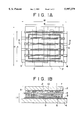
- FIGS. 1A and 1B are a plan view and a sectional view, respectively, of an embodiment representing the plasma addressed liquid crystal display device of the present invention
- FIG. 2 is a process diagram illustrating an essential step in a method for manufacture of the plasma addressed liquid crystal display device of the present invention
- FIG. 3 is a partial sectional view showing a reference example of a plasma addressed liquid crystal display device.
- FIG. 4 is a sectional view showing a general construction of a conventional plasma addressed liquid crystal display device in the prior art.
- FIGS. 1A and 1B are a plan view and a sectional view each showing an exemplary construction of the plasma addressed liquid crystal display device of the present invention.
- This display device has a flat panel structure where a liquid crystal cell is superposed on a plasma cell.
- the liquid crystal cell consists of a front substrate 2 of glass or the like where data electrodes 1 are arranged in columns.
- the front substrate 2 is bonded to an intermediate substrate with a predetermined gap retained therebetween.
- the intermediate substrate is composed of an extremely thin glass sheet or the like. And the gap defined between the front substrate 2 and the intermediate substrate is filled with a liquid crystal.
- the data electrodes 1 are extended alternately up to both ends of the front substrate 2 so as to be electrically connected to external circuits.
- the plasma cell consists of a rear substrate 4 where discharge electrodes 3 are arranged in rows.
- the rear substrate 4 is also composed of a glass sheet or the like.
- the discharge electrodes 3 are extended alternately up to both left and right ends of the rear substrate 4 so as to be electrically connected to external circuits.
- Barrier ribs 5 are formed in a manner to match to the discharge electrodes 3 respectively.
- the rear substrate 4 is joined to the intermediate substrate via a predetermined space by the use of glass frit 6. In this case, the respective top portions of the barrier ribs 5 abut on the rear surface of the intermediate substrate, so that the space is divided into stripes to thereby prescribe discharge channels. And at both left and right ends of each barrier rib 5, notches are formed as regions to be coated with the glass frits 6.
- the data electrodes 1 and the discharge electrodes 3 be exposed from the ends of the relevant substrates respectively, and therefore the front substrate 2 and the rear substrate 4 are shaped to be different from each other to meet the above requirement.
- One of the requisites of the present invention is that the area of the intermediate substrate is dimensionally so set as to include the overlapping planar region of the front substrate 2 and the rear substrate 4 which are mutually different in shape.
- the area of the intermediate substrate is excessively large, there may arise some impediment to connection of the electrodes to external circuits. It is therefore preferred that the area be matched substantially to the overlapping planar region.
- the plasma addressed liquid crystal display device has a height (H) of 250 mm and a width (W) of 300 mm, while the overlapping planar region of the front substrate 2 and the rear substrate 4 has a height (h) of 230 mm and a width (w) of 270 mm.
- FIG. 1B is a sectional view showing the structure of the plasma addressed liquid crystal display device taken along the line B--B in FIG. 1A.
- the front substrate 2 is bonded onto the upper surface of the intermediate substrate 8 via a sealant 7 to thereby constitute the aforementioned liquid crystal cell 9.
- spacer particles 10 for dimensionally prescribing the gap in the liquid cell 9 are existent over the planar region described above.
- the rear substrate 4 is joined to the lower surface of the intermediate substrate 8 via the glass frit 6 to thereby constitute the aforementioned plasma cell 11.
- a plurality of barrier ribs 5 for dimensionally prescribing the space in the plasma cell 11 are existent over the planar region, so that the intermediate substrate 8 is supported uniformly by the spacer particles 10 and the barrier ribs 5 from above and below. Since the gap in the liquid cell 9 is dimensionally determined merely by the size of the spacer particles 10, a uniform thickness of the liquid crystal cell can be ensured over the entire planar region by hardening the sealant 7 while applying a uniform load in this state.
- the sealant 7 may be composed of ultraviolet-setting resin for example.
- Exemplary dimensions of the individual component members are such that each of the spacer particles 10 has a diameter of 5.0 ⁇ m, the intermediate substrate 8 of a thin glass sheet has a thickness of 50 ⁇ m, each of the barrier ribs 5 has a height of 200 ⁇ m or so, and the front substrate 2 has a thickness of 1.1 mm.
- a plasma cell 11 is assembled by joining a rear substrate 4, where row discharge electrodes 3 and barrier ribs 5 are formed previously, to one surface of an intermediate substrate 8 having a predetermined area. Glass frit 6 is used for joining the two substrates to each other. Thereafter a front substrate 2, where column data electrodes 1 are formed previously, is disposed opposite to the other surface of the intermediate substrate 8, and a flat panel structure is assembled by superposing these two substrates mutually in a state where spacer particles 10 and an ultraviolet-setting sealant 7 are interposed therebetween.
- the flat panel structure is inserted into a gastight enclosure and, by evacuation of such enclosure, a uniform atmospheric pressure is applied to the flat panel structure from above and below. Then ultraviolet rays are irradiated in this state to harden the sealant 7 to thereby bond the front substrate 2 and the intermediate substrate 8 to each other. And finally a liquid crystal 12 is injected into the gap prescribed by the spacer particles 10 between the front substrate 2 and the intermediate substrate 8 to consequently produce a liquid crystal cell.
- FIG. 2 typically illustrates a liquid crystal assembling step which is essential in the manufacturing method of the present invention.
- a flat panel 13 is inserted into a gastight enclosure 14, which is then evacuated so that a uniform load is applied to the flat panel from above and below.
- ultraviolet rays (UV) are irradiated to harden the sealant 7, thereby bonding the front substrate 2 and the intermediate substrate 8 to each other.
- the thickness of the liquid crystal cell including the periphery of the panel 13 was rendered uniform as 5.0 ⁇ 0.1 ⁇ m. It is generally necessary for the characteristics of a liquid crystal cell to ensure a precision of ⁇ 0.1 ⁇ m, and the manufacturing method of the invention is capable of completely achieving the desired precision.
- the gastight enclosure 14 may be composed of a film or the like, and a preferred material thereof is polyethylene for example. Since polyethylene is sufficiently adequate for transmitting ultraviolet rays therethrough, it becomes possible to execute the process of hardening the sealant 7 while keeping the flat panel 13 inserted in the gastight enclosure 14.
- the vacuum pressure means adopted in the present invention is free from causing any crack or the like in the glass material of the substrate, since the flat panel 13 is inserted in the flexible gastight enclosure 14 and a uniform atmospheric pressure is applied thereto from an ambience.
- FIG. 3 is a partial sectional view typically showing a reference example of a plasma addressed liquid crystal display device.
- any component elements corresponding to those in the plasma addressed liquid crystal display device of the present invention shown in FIG. 1B are denoted by like reference numerals.
- the area of an intermediate substrate 8 is dimensionally smaller than an overlapping planar region of a front substrate 2 and a rear substrate 4.
- a pressure is applied to an end portion of the front substrate 2 to consequently cause deformation of the end portion.
- the gap dimension is varied considerably in a range of 5.0 ⁇ 1.0 ⁇ m or so.
- the intermediate substrate 8 is positioned inside the end portion of the front substrate 2, the end portion of the front substrate 2 is not supported uniformly by dummy barrier ribs 5a positioned in the outermost portion of the rear substrate 4, so that the deformation and strain mentioned are left there.
- the area of an intermediate substrate is dimensionally so set as to include an overlapping planar region of a front substrate and a rear substrate which are different in shape from each other. Spacer particles are existent between the intermediate substrate and the front substrate over the planar region, and barrier ribs are existent between the intermediate substrate and the rear substrate similarly over the planar region. Due to such a structure, the gap dimension in the liquid crystal cell can be controlled uniformly without inducing breakage of the intermediate substrate. Further according to the present invention, a flat panel is inserted into a gastight enclosure, and a sealant is hardened after evacuation of the gastight enclosure and application of a uniform atmospheric pressure to the flat panel from above and below. Consequently, it becomes possible to ensure a uniform gap dimension in the liquid crystal cell while preventing breakage of the intermediate substrate.
Abstract
A plasma addressed liquid crystal display device having a flat panel structure where a liquid crystal cell is superposed on a plasma cell. The liquid crystal cell comprises a front substrate with data electrodes arranged in columns, an intermediate substrate bonded to the front substrate via a predetermined gap, and a liquid crystal filled in the gap. The plasma cell comprises a rear substrate joined to the intermediate substrate via a predeter- mined space, and discharge channels formed in the space and arranged in rows. The intermediate substrate is dimensionally so set as to include an overlapping planar region of the front substrate and the rear substrate which are different in shape from each other. And spacer particles for prescribing the gap dimension in the liquid crystal cell are existent between the intermediate and front substrates over the planar region. Further a plurality of barrier ribs for prescribing the space dimension in the plasma cell are existent between the intermediate and rear substrates over the planar region. In this display device, the gap in the liquid crystal cell is rendered dimensionally uniform, and breakage of the intermediate substrate is preventable.
Description
This is a divisional of application Ser. No. 08/932,340 filed Sep. 17, 1997, now U.S. Pat. No. 5,886,467, which is a continuation of Ser. No. 08/566,173, filed Dec. 1, 1995, now abandoned.
1. Field of the Invention
The present invention relates to a plasma addressed liquid crystal display device having a flat panel structure where a liquid crystal cell is superposed on a plasma cell, and more particularly to the shape of an intermediate substrate (microsheet) disposed between a liquid crystal cell and a plasma cell for separating them from each other. Further the invention relates also to a processing technique adopted in assembling a liquid crystal cell on a plasma cell.
2. Description of the Related Art
There is known a plasma addressed display device where a plasma cell is utilized for addressing a liquid crystal cell, as disclosed for example in Japanese Patent Laid-open No. Hei 4-265931 which corresponds to U.S. patent application Ser. No. 07/837,961 for an Electro Optical Device, filed by Shigeki Miyazaki on Feb. 20, 1992. As shown in FIG. 4, the above plasma addressed display device has a flat panel structure comprising a liquid crystal cell 101, a plasma cell 102 and a common intermediate substrate 103 interposed therebetween. The intermediate substrate 103 is composed of an extremely thin glass sheet or the like and is termed a microsheet. The plasma cell 102 consists of a rear substrate 104 joined to the intermediate substrate 103, and an ionizable gas is contained hermetically in a space defined therebetween. Striped discharge electrodes 105 are formed on an inner surface of the rear substrate 104. Since the discharge electrodes 105 can be produced through print baking on the flat rear substrate 104 by a screen printing process or the like, it is possible to attain superior productivity and workability with another advantage of adequacy for miniaturization. Barrier ribs 106 are formed on the discharge electrodes 105 to divide the space where the ionizable gas is hermetically contained, thereby constituting discharge channels 107. The barrier ribs 106 can also be baked by a screen printing process, and the respective tops thereof abut on one surface of the intermediate substrate 103. The striped discharge electrodes 105 function as anodes A and cathodes K alternately to generate plasma discharge therebetween. The intermediate substrate 103 and the rear substrate 104 are joined to each other by the use of glass frit 108 or the like.
Meanwhile the liquid crystal cell 101 is composed of a transparent front substrate 109. The front substrate 109 is bonded to the other surface of the intermediate substrate 103 with a predetermined gap retained therebetween by the use of a sealant 110 or the like, and the gap is filled with a liquid crystal 111. Data electrodes 112 are formed on the inner surface of the front substrate 109 in a manner to be orthogonal to the striped discharge electrodes 105. And matrix pixels are prescribed at the intersections of the data electrodes 112 and the discharge channels 107.
In the plasma addressed display device of the structure mentioned above, display driving is performed by line-sequentially switching and scanning the row discharge channels 107 where plasma discharges are generated and simultaneously applying, in synchronism with the scanning, picture signals to the column data electrodes 112 on the side of the liquid crystal cell 101. Upon generation of plasma discharges in the discharge channels 107, the inside is turned to the anode potential substantially uniformly, and the pixels are selected per row. That is, each discharge channel functions as a sampling switch. When a picture signal is applied to each pixel in a conducting state of the plasma sampling switch, the sampled pixel can be turn on or off under control. And even after the plasma sampling switch is turned to its non-conducting state, the picture signal is still held in the related pixel.
The intermediate substrate 103, which physically separates the liquid crystal cell 101 and the plasma cell 102 from each other, has an extremely small thickness of 50 μm or so for electrically coupling the two cells. Therefore the intermediate substrate 103 is termed a microsheet. The front substrate 109 is bonded onto such microsheet through the sealant 110 with a gap retained therebetween, and the gap is filled with the liquid crystal 111 hermetically to constitute the liquid crystal cell 101. This gap has a further smaller dimension of 5 μm or so. And for the purpose of ensuring a stable superior picture quality on the display, it is requisite to achieve uniform dimensional control of the gap over the entire display area. However, it has been difficult heretofore to realize satisfactory uniform control of the gap dimension.
It is an object of the present invention to provide an improved plasma addressed liquid crystal display device wherein the gap dimension in a liquid crystal cell is rendered uniform by modifying the shape of an intermediate substrate.
And another object of the present invention resides in preventing breakage of the intermediate substrate in view of the conventional disadvantage that, since the intermediate substrate is composed of an extremely thin glass microsheet, it is frequently prone to be cracked or broken in a step of assembling the liquid crystal cell.
According to one aspect of the present invention, there is provided a plasma addressed liquid crystal display device having a flat panel structure where a liquid crystal cell is superposed on a plasma cell. The liquid crystal cell comprises a front substrate with data electrodes arranged in columns, an intermediate substrate bonded to the front substrate via a predetermined gap, and a liquid crystal filled in the gap. The plasma cell comprises a rear substrate joined to the intermediate substrate via a predetermined space, and discharge channels formed in the space and arranged in rows. The requisites of the invention reside in that the area of the intermediate substrate is dimensionally so set that the overlapping planar region of the front substrate and the rear substrate of mutually different external shapes is included in the intermediate substrate. And spacer particles for prescribing the gap dimension in the liquid crystal cell are existent between the intermediate and front substrates over the planar region. Further a plurality of barrier ribs for prescribing the space dimensions in the plasma cell are existent between the intermediate and rear substrates over the planar region.
According to another aspect of the present invention, there is provided a method of manufacturing a plasma addressed liquid crystal display device having the above construction. The method comprises a first step of assembling a plasma cell by joining a rear substrate, where row discharge electrodes and barrier ribs are previously formed, to one surface of an intermediate substrate having a predetermined area; a second step of assembling a flat panel structure by disposing a front substrate, where column data electrodes are previously formed, opposite to the other surface of the intermediate substrate, and superposing the mutually opposite substrates with spacer particles and a sealant interposed therebetween; a third step of inserting the flat panel structure into a gastight enclosure, then vacuuming the enclosure and, while applying an atmospheric pressure uniformly to the flat panel structure from above and below, hardening the sealant in this state to thereby bond the front substrate and the intermediate substrate to each other; and a fourth step of producing a liquid crystal cell by injecting a liquid crystal into the gap prescribed by the spacer particles between the front and intermediate substrates.
In the present invention, the screen of the plasma addressed liquid crystal display device is composed of the overlapping planar region of the front substrate and the rear substrate having mutually different shapes. The area of the intermediate substrate disposed between the front and rear substrates is dimensionally so set as to include the planar region. Preferably, the area of the intermediate substrate is dimensionally so set as to match to the planar region substantially. And the spacer particles are existent between the intermediate and front substrates over the planar region, and also the barrier ribs are existent between the intermediate and rear substrates over the planar region. Due to the above structure, it becomes possible to attain uniform dimensional control of the gap between the intermediate and front substrates over the entire effective screen of the display device. Furthermore, in the step of assembling the liquid crystal cell by bonding the front substrate to the intermediate substrate, the flat panel structure is inserted into a gastight enclosure and, after evacuation thereof, the atmospheric pressure is applied thereto uniformly from above and below, and the sealant is hardened by irradiation of ultraviolet rays or the like. Consequently, uniform application of the pressure from the ambience to the front and rear substrates can be achieved to thereby prevent breakage of the intermediate substrate while rendering the gap dimension uniform.
The above and other features and advantages of the present invention will become apparent from the following description which will be given with reference to the illustrative accompanying drawings.
FIGS. 1A and 1B are a plan view and a sectional view, respectively, of an embodiment representing the plasma addressed liquid crystal display device of the present invention;
FIG. 2 is a process diagram illustrating an essential step in a method for manufacture of the plasma addressed liquid crystal display device of the present invention;
FIG. 3 is a partial sectional view showing a reference example of a plasma addressed liquid crystal display device; and
FIG. 4 is a sectional view showing a general construction of a conventional plasma addressed liquid crystal display device in the prior art.
Hereinafter preferred embodiments of the present invention will be described in detail with reference to the accompanying drawings. FIGS. 1A and 1B are a plan view and a sectional view each showing an exemplary construction of the plasma addressed liquid crystal display device of the present invention. This display device has a flat panel structure where a liquid crystal cell is superposed on a plasma cell. As shown in FIG. 1A, the liquid crystal cell consists of a front substrate 2 of glass or the like where data electrodes 1 are arranged in columns. The front substrate 2 is bonded to an intermediate substrate with a predetermined gap retained therebetween. The intermediate substrate is composed of an extremely thin glass sheet or the like. And the gap defined between the front substrate 2 and the intermediate substrate is filled with a liquid crystal. The data electrodes 1 are extended alternately up to both ends of the front substrate 2 so as to be electrically connected to external circuits. Meanwhile the plasma cell consists of a rear substrate 4 where discharge electrodes 3 are arranged in rows. The rear substrate 4 is also composed of a glass sheet or the like. And similarly the discharge electrodes 3 are extended alternately up to both left and right ends of the rear substrate 4 so as to be electrically connected to external circuits. Barrier ribs 5 are formed in a manner to match to the discharge electrodes 3 respectively. The rear substrate 4 is joined to the intermediate substrate via a predetermined space by the use of glass frit 6. In this case, the respective top portions of the barrier ribs 5 abut on the rear surface of the intermediate substrate, so that the space is divided into stripes to thereby prescribe discharge channels. And at both left and right ends of each barrier rib 5, notches are formed as regions to be coated with the glass frits 6.
For the purpose of connection to external circuits, it is necessary that the data electrodes 1 and the discharge electrodes 3 be exposed from the ends of the relevant substrates respectively, and therefore the front substrate 2 and the rear substrate 4 are shaped to be different from each other to meet the above requirement. One of the requisites of the present invention is that the area of the intermediate substrate is dimensionally so set as to include the overlapping planar region of the front substrate 2 and the rear substrate 4 which are mutually different in shape. However, if the area of the intermediate substrate is excessively large, there may arise some impediment to connection of the electrodes to external circuits. It is therefore preferred that the area be matched substantially to the overlapping planar region. In a concrete example, specific dimensions are so set that the plasma addressed liquid crystal display device has a height (H) of 250 mm and a width (W) of 300 mm, while the overlapping planar region of the front substrate 2 and the rear substrate 4 has a height (h) of 230 mm and a width (w) of 270 mm.
FIG. 1B is a sectional view showing the structure of the plasma addressed liquid crystal display device taken along the line B--B in FIG. 1A. As shown, the front substrate 2 is bonded onto the upper surface of the intermediate substrate 8 via a sealant 7 to thereby constitute the aforementioned liquid crystal cell 9. Between the intermediate substrate 8 and the front substrate 2, spacer particles 10 for dimensionally prescribing the gap in the liquid cell 9 are existent over the planar region described above. Meanwhile the rear substrate 4 is joined to the lower surface of the intermediate substrate 8 via the glass frit 6 to thereby constitute the aforementioned plasma cell 11. Between the intermediate substrate 8 and the rear substrate 4, a plurality of barrier ribs 5 for dimensionally prescribing the space in the plasma cell 11 are existent over the planar region, so that the intermediate substrate 8 is supported uniformly by the spacer particles 10 and the barrier ribs 5 from above and below. Since the gap in the liquid cell 9 is dimensionally determined merely by the size of the spacer particles 10, a uniform thickness of the liquid crystal cell can be ensured over the entire planar region by hardening the sealant 7 while applying a uniform load in this state. The sealant 7 may be composed of ultraviolet-setting resin for example. Exemplary dimensions of the individual component members are such that each of the spacer particles 10 has a diameter of 5.0 μm, the intermediate substrate 8 of a thin glass sheet has a thickness of 50 μm, each of the barrier ribs 5 has a height of 200 μm or so, and the front substrate 2 has a thickness of 1.1 mm.
Referring now to FIG. 1B continuously, a detailed description will be given on a method for manufacture of the plasma addressed liquid crystal display device of the invention. First a plasma cell 11 is assembled by joining a rear substrate 4, where row discharge electrodes 3 and barrier ribs 5 are formed previously, to one surface of an intermediate substrate 8 having a predetermined area. Glass frit 6 is used for joining the two substrates to each other. Thereafter a front substrate 2, where column data electrodes 1 are formed previously, is disposed opposite to the other surface of the intermediate substrate 8, and a flat panel structure is assembled by superposing these two substrates mutually in a state where spacer particles 10 and an ultraviolet-setting sealant 7 are interposed therebetween. Subsequently the flat panel structure is inserted into a gastight enclosure and, by evacuation of such enclosure, a uniform atmospheric pressure is applied to the flat panel structure from above and below. Then ultraviolet rays are irradiated in this state to harden the sealant 7 to thereby bond the front substrate 2 and the intermediate substrate 8 to each other. And finally a liquid crystal 12 is injected into the gap prescribed by the spacer particles 10 between the front substrate 2 and the intermediate substrate 8 to consequently produce a liquid crystal cell.
FIG. 2 typically illustrates a liquid crystal assembling step which is essential in the manufacturing method of the present invention. As illustrated, a flat panel 13 is inserted into a gastight enclosure 14, which is then evacuated so that a uniform load is applied to the flat panel from above and below. In this state, ultraviolet rays (UV) are irradiated to harden the sealant 7, thereby bonding the front substrate 2 and the intermediate substrate 8 to each other. According to the experimental result, the thickness of the liquid crystal cell including the periphery of the panel 13 was rendered uniform as 5.0±0.1 μm. It is generally necessary for the characteristics of a liquid crystal cell to ensure a precision of ±0.1 μm, and the manufacturing method of the invention is capable of completely achieving the desired precision. The gastight enclosure 14 may be composed of a film or the like, and a preferred material thereof is polyethylene for example. Since polyethylene is sufficiently adequate for transmitting ultraviolet rays therethrough, it becomes possible to execute the process of hardening the sealant 7 while keeping the flat panel 13 inserted in the gastight enclosure 14.
Instead of the above-described vacuum pressure means using a gastight enclosure, there may be contrived another means which positions a flat panel 13 on a surface table and applies pressure thereto by placing a weight from above to join the front substrate 2 to the intermediate substrate 8. However, in the case of a plasma addressed liquid crystal display device where discharge electrodes and barrier ribs 5 are baked previously on the rear substrate 4 by a screen printing process, some warps and undulations are caused on the rear substrate 4 during the baking process by the difference between the thermal expansion coefficients and so forth. Consequently, if a weight is placed from above in the state where the flat panel is positioned on a surface table, there may occur a fault that many cracks or flaws are induced in the glass. In contrast therewith, the vacuum pressure means adopted in the present invention is free from causing any crack or the like in the glass material of the substrate, since the flat panel 13 is inserted in the flexible gastight enclosure 14 and a uniform atmospheric pressure is applied thereto from an ambience.
FIG. 3 is a partial sectional view typically showing a reference example of a plasma addressed liquid crystal display device. For the purpose of making this example better understood, any component elements corresponding to those in the plasma addressed liquid crystal display device of the present invention shown in FIG. 1B are denoted by like reference numerals. In this example, the area of an intermediate substrate 8 is dimensionally smaller than an overlapping planar region of a front substrate 2 and a rear substrate 4. In this construction, there is a disadvantage that when the front substrate 2 is bonded to the intermediate substrate 8, a pressure is applied to an end portion of the front substrate 2 to consequently cause deformation of the end portion. And if a sealant 7 is hardened in this state, some strain is left as illustrated to eventually fail in attaining a dimensionally uniform gap in a liquid crystal cell 9. In this reference example, the gap dimension is varied considerably in a range of 5.0±1.0 μm or so. In case the intermediate substrate 8 is positioned inside the end portion of the front substrate 2, the end portion of the front substrate 2 is not supported uniformly by dummy barrier ribs 5a positioned in the outermost portion of the rear substrate 4, so that the deformation and strain mentioned are left there.
According to the present invention, as described hereinabove, the area of an intermediate substrate is dimensionally so set as to include an overlapping planar region of a front substrate and a rear substrate which are different in shape from each other. Spacer particles are existent between the intermediate substrate and the front substrate over the planar region, and barrier ribs are existent between the intermediate substrate and the rear substrate similarly over the planar region. Due to such a structure, the gap dimension in the liquid crystal cell can be controlled uniformly without inducing breakage of the intermediate substrate. Further according to the present invention, a flat panel is inserted into a gastight enclosure, and a sealant is hardened after evacuation of the gastight enclosure and application of a uniform atmospheric pressure to the flat panel from above and below. Consequently, it becomes possible to ensure a uniform gap dimension in the liquid crystal cell while preventing breakage of the intermediate substrate.
Although the present invention has been explained with reference to the preferred embodiments thereof, it is to be understood that the invention is not limited to such embodiments alone, and a variety of other modifications and variations will be apparent to those skilled in the art without departing from the spirit of the invention.
The scope of the invention, therefore, is to be determined solely by the appended claims.
Claims (1)
1. A method of manufacturing a plasma addressed liquid crystal display device, comprising the steps of:
providing an intermediate substrate on a rear substrate having a plurality of discharge electrodes arranged in parallel to each other;
disposing a front substrate opposite to said intermediate substrate with a gap retained therebetween, said front substrate comprising a plurality of data electrodes arranged in parallel to each other and perpendicular to the discharge electrodes;
constructing said front, intermediate and rear substrates integrally by sealing up said gap;
providing a plurality of particles of gap spacer between said front and intermediate substrates;
inserting a display panel into a gastight enclosure composed of a film or the like;
vacuuming said gastight enclosure where said display panel is inserted; and
providing a liquid crystal between said front and intermediate substrates.
Priority Applications (1)
| Application Number | Priority Date | Filing Date | Title |
|---|---|---|---|
| US09/252,156 US5997379A (en) | 1994-12-02 | 1999-02-18 | Method of manufacturing plasma addressed liquid crystal display |
Applications Claiming Priority (5)
| Application Number | Priority Date | Filing Date | Title |
|---|---|---|---|
| JPP06-329446 | 1994-12-02 | ||
| JP6329446A JPH08160401A (en) | 1994-12-02 | 1994-12-02 | Plasma address display element and its production |
| US56617395A | 1995-12-01 | 1995-12-01 | |
| US08/932,340 US5886467A (en) | 1994-12-02 | 1997-09-17 | Plasma addressed liquid crystal display device |
| US09/252,156 US5997379A (en) | 1994-12-02 | 1999-02-18 | Method of manufacturing plasma addressed liquid crystal display |
Related Parent Applications (1)
| Application Number | Title | Priority Date | Filing Date |
|---|---|---|---|
| US08/932,340 Division US5886467A (en) | 1994-12-02 | 1997-09-17 | Plasma addressed liquid crystal display device |
Publications (1)
| Publication Number | Publication Date |
|---|---|
| US5997379A true US5997379A (en) | 1999-12-07 |
Family
ID=18221471
Family Applications (2)
| Application Number | Title | Priority Date | Filing Date |
|---|---|---|---|
| US08/932,340 Expired - Fee Related US5886467A (en) | 1994-12-02 | 1997-09-17 | Plasma addressed liquid crystal display device |
| US09/252,156 Expired - Fee Related US5997379A (en) | 1994-12-02 | 1999-02-18 | Method of manufacturing plasma addressed liquid crystal display |
Family Applications Before (1)
| Application Number | Title | Priority Date | Filing Date |
|---|---|---|---|
| US08/932,340 Expired - Fee Related US5886467A (en) | 1994-12-02 | 1997-09-17 | Plasma addressed liquid crystal display device |
Country Status (4)
| Country | Link |
|---|---|
| US (2) | US5886467A (en) |
| JP (1) | JPH08160401A (en) |
| KR (1) | KR960024544A (en) |
| CN (1) | CN1150656A (en) |
Cited By (6)
| Publication number | Priority date | Publication date | Assignee | Title |
|---|---|---|---|---|
| US6247985B1 (en) * | 2000-08-28 | 2001-06-19 | Larry A. Block | Surfboard box cover |
| US6330049B1 (en) * | 1998-03-25 | 2001-12-11 | Sharp Kabushiki Kaisha | Liquid crystal display device, and method for producing the same |
| US6590332B1 (en) * | 1999-08-06 | 2003-07-08 | Samsung Sdi Co., Ltd. | Plasma display panel including front and rear substrate assemblies |
| US20040158977A1 (en) * | 2000-11-10 | 2004-08-19 | Seiko Epson Corporation | Optical device and method of manufacture thereof, and electronic instrument |
| US20040177498A1 (en) * | 2000-12-18 | 2004-09-16 | Tdk Corporation | Electronic device and manufacturing same |
| US6827623B2 (en) * | 1998-06-29 | 2004-12-07 | Fujitsu Limited | Manufacturing method of plasma display panels |
Families Citing this family (8)
| Publication number | Priority date | Publication date | Assignee | Title |
|---|---|---|---|---|
| US6137550A (en) * | 1996-09-30 | 2000-10-24 | Tektronix, Inc. | Structure for a PALC display panel having a helium filling doped with hydrogen |
| JP3849735B2 (en) * | 1997-04-10 | 2006-11-22 | 株式会社日立プラズマパテントライセンシング | Plasma display panel and manufacturing method thereof |
| JP3481843B2 (en) * | 1997-12-26 | 2003-12-22 | シャープ株式会社 | Liquid crystal display |
| JP3569458B2 (en) * | 1999-03-26 | 2004-09-22 | パイオニア株式会社 | Plasma display panel |
| KR100522686B1 (en) * | 2002-11-05 | 2005-10-19 | 삼성에스디아이 주식회사 | Plasma display panel |
| FR2847996B1 (en) * | 2002-11-28 | 2005-10-07 | Thales Sa | DEDICATED DISPLAY DEVICE WITH PROXIMITY DETECTION |
| KR100868413B1 (en) * | 2002-12-27 | 2008-11-11 | 오리온피디피주식회사 | Multi plasma display panel |
| JP4482637B2 (en) * | 2004-04-26 | 2010-06-16 | Nec液晶テクノロジー株式会社 | Liquid crystal display |
Citations (10)
| Publication number | Priority date | Publication date | Assignee | Title |
|---|---|---|---|---|
| US4139250A (en) * | 1975-10-27 | 1979-02-13 | U.S. Philips Corporation | Gas discharge display panel and method of manufacturing the same |
| US4526818A (en) * | 1982-12-23 | 1985-07-02 | Epson Corporation | Liquid crystal display panel and process for the production thereof |
| DE4223304A1 (en) * | 1991-10-26 | 1993-04-29 | Samsung Electronic Devices | PLASMA ADDRESSED LIQUID CRYSTAL DISPLAY |
| US5207607A (en) * | 1990-04-11 | 1993-05-04 | Mitsubishi Denki Kabushiki Kaisha | Plasma display panel and a process for producing the same |
| DE4211258A1 (en) * | 1991-10-29 | 1993-05-06 | Samsung Electron Devices Co., Ltd., Kyonggi, Kr | PLASMA-ADDRESSED LIQUID CRYSTAL DISPLAY AND PRODUCTION METHOD FOR THE SAME |
| DE4306305A1 (en) * | 1992-04-30 | 1993-11-04 | Samsung Electronic Devices | A LIQUID CRYSTAL DISPLAY USING PLASMA ADDRESSING AND CONTROL METHOD FOR THE SAME |
| DE4239149A1 (en) * | 1992-05-26 | 1993-12-02 | Samsung Electronic Devices | Plasma addressed liquid crystal display panel e.g for HDTV - has front phase and back plate enclosing liquid crystal section with plasma space filled with discharge gas. |
| EP0597432A1 (en) * | 1992-11-09 | 1994-05-18 | Sony Corporation | Plasma addressed liquid crystal display device |
| US5351144A (en) * | 1992-02-04 | 1994-09-27 | Sony Corporation | Plasma addressed electro-optical device with non-continuous barrier ribs |
| US5428263A (en) * | 1992-01-07 | 1995-06-27 | Mitsubishi Denki Kabushiki Kaisha | Discharge cathode device with stress relieving layer and method for manufacturing the same |
-
1994
- 1994-12-02 JP JP6329446A patent/JPH08160401A/en active Pending
-
1995
- 1995-12-01 KR KR19950045997A patent/KR960024544A/ko not_active Application Discontinuation
- 1995-12-01 CN CN95120032A patent/CN1150656A/en active Pending
-
1997
- 1997-09-17 US US08/932,340 patent/US5886467A/en not_active Expired - Fee Related
-
1999
- 1999-02-18 US US09/252,156 patent/US5997379A/en not_active Expired - Fee Related
Patent Citations (10)
| Publication number | Priority date | Publication date | Assignee | Title |
|---|---|---|---|---|
| US4139250A (en) * | 1975-10-27 | 1979-02-13 | U.S. Philips Corporation | Gas discharge display panel and method of manufacturing the same |
| US4526818A (en) * | 1982-12-23 | 1985-07-02 | Epson Corporation | Liquid crystal display panel and process for the production thereof |
| US5207607A (en) * | 1990-04-11 | 1993-05-04 | Mitsubishi Denki Kabushiki Kaisha | Plasma display panel and a process for producing the same |
| DE4223304A1 (en) * | 1991-10-26 | 1993-04-29 | Samsung Electronic Devices | PLASMA ADDRESSED LIQUID CRYSTAL DISPLAY |
| DE4211258A1 (en) * | 1991-10-29 | 1993-05-06 | Samsung Electron Devices Co., Ltd., Kyonggi, Kr | PLASMA-ADDRESSED LIQUID CRYSTAL DISPLAY AND PRODUCTION METHOD FOR THE SAME |
| US5428263A (en) * | 1992-01-07 | 1995-06-27 | Mitsubishi Denki Kabushiki Kaisha | Discharge cathode device with stress relieving layer and method for manufacturing the same |
| US5351144A (en) * | 1992-02-04 | 1994-09-27 | Sony Corporation | Plasma addressed electro-optical device with non-continuous barrier ribs |
| DE4306305A1 (en) * | 1992-04-30 | 1993-11-04 | Samsung Electronic Devices | A LIQUID CRYSTAL DISPLAY USING PLASMA ADDRESSING AND CONTROL METHOD FOR THE SAME |
| DE4239149A1 (en) * | 1992-05-26 | 1993-12-02 | Samsung Electronic Devices | Plasma addressed liquid crystal display panel e.g for HDTV - has front phase and back plate enclosing liquid crystal section with plasma space filled with discharge gas. |
| EP0597432A1 (en) * | 1992-11-09 | 1994-05-18 | Sony Corporation | Plasma addressed liquid crystal display device |
Cited By (8)
| Publication number | Priority date | Publication date | Assignee | Title |
|---|---|---|---|---|
| US6330049B1 (en) * | 1998-03-25 | 2001-12-11 | Sharp Kabushiki Kaisha | Liquid crystal display device, and method for producing the same |
| US6827623B2 (en) * | 1998-06-29 | 2004-12-07 | Fujitsu Limited | Manufacturing method of plasma display panels |
| US6590332B1 (en) * | 1999-08-06 | 2003-07-08 | Samsung Sdi Co., Ltd. | Plasma display panel including front and rear substrate assemblies |
| US6247985B1 (en) * | 2000-08-28 | 2001-06-19 | Larry A. Block | Surfboard box cover |
| US20040158977A1 (en) * | 2000-11-10 | 2004-08-19 | Seiko Epson Corporation | Optical device and method of manufacture thereof, and electronic instrument |
| US7096579B2 (en) * | 2000-11-10 | 2006-08-29 | Seiko Epson Corporation | Method of manufacturing an optical device |
| US20040177498A1 (en) * | 2000-12-18 | 2004-09-16 | Tdk Corporation | Electronic device and manufacturing same |
| US7134196B2 (en) * | 2000-12-18 | 2006-11-14 | Tdk Corporation | Electronic device and manufacturing same |
Also Published As
| Publication number | Publication date |
|---|---|
| US5886467A (en) | 1999-03-23 |
| JPH08160401A (en) | 1996-06-21 |
| KR960024544A (en) | 1996-07-20 |
| CN1150656A (en) | 1997-05-28 |
Similar Documents
| Publication | Publication Date | Title |
|---|---|---|
| US5997379A (en) | Method of manufacturing plasma addressed liquid crystal display | |
| JPH05134242A (en) | Plasma-address type liquid crystal display element and manufacture thereof | |
| US6166711A (en) | Plasma addressed electro-optical display | |
| US5772486A (en) | Method for manufacturing a plasma-addressed display device | |
| US6545410B1 (en) | Flat panel display of a sealing channel | |
| JPH08313887A (en) | Plasma address display panel and its production | |
| US5670843A (en) | Plasma addressed display device | |
| US5844639A (en) | Plasma addressed liquid crystal display device | |
| US5914562A (en) | Anodic bonded plasma addressed liquid crystal displays | |
| US5684362A (en) | Plasma addressed electro-optical device having a plasma discharge chamber | |
| KR100229246B1 (en) | Plasma address liquid crystal display | |
| JP3366026B2 (en) | Plasma address electro-optical device | |
| US5923389A (en) | Plasma addressed electro-optical display | |
| US6257945B1 (en) | Method for sealing a gas within a picture display device | |
| US5886463A (en) | Thin-type display device with one-piece rear wall | |
| JPH05297810A (en) | Manufacture of plasma address electrooptic device | |
| KR100399299B1 (en) | Manufacturing Method of Plasma Address Display Device | |
| JP3430666B2 (en) | Plasma address display device and method of manufacturing the same | |
| JPH0668801A (en) | Plasma discharge panel | |
| JPH05216416A (en) | Plasma address electrooptical device | |
| JPH11237613A (en) | Plasma address display device | |
| JPH08313889A (en) | Display panel | |
| JPH08304790A (en) | Production of plasma address display device | |
| JPH10133192A (en) | Display device | |
| JPH11218741A (en) | Frit seal structure for plasma address liquid crystal display element |
Legal Events
| Date | Code | Title | Description |
|---|---|---|---|
| REMI | Maintenance fee reminder mailed | ||
| LAPS | Lapse for failure to pay maintenance fees | ||
| FP | Lapsed due to failure to pay maintenance fee |
Effective date: 20031207 |
|
| STCH | Information on status: patent discontinuation |
Free format text: PATENT EXPIRED DUE TO NONPAYMENT OF MAINTENANCE FEES UNDER 37 CFR 1.362 |