US6005443A - Phase locked loop frequency synthesizer for multi-band application - Google Patents
Phase locked loop frequency synthesizer for multi-band application Download PDFInfo
- Publication number
- US6005443A US6005443A US09/044,281 US4428198A US6005443A US 6005443 A US6005443 A US 6005443A US 4428198 A US4428198 A US 4428198A US 6005443 A US6005443 A US 6005443A
- Authority
- US
- United States
- Prior art keywords
- output
- frequency
- vco
- phase detector
- value
- Prior art date
- Legal status (The legal status is an assumption and is not a legal conclusion. Google has not performed a legal analysis and makes no representation as to the accuracy of the status listed.)
- Expired - Lifetime
Links
Images


Classifications
-
- H—ELECTRICITY
- H04—ELECTRIC COMMUNICATION TECHNIQUE
- H04B—TRANSMISSION
- H04B1/00—Details of transmission systems, not covered by a single one of groups H04B3/00 - H04B13/00; Details of transmission systems not characterised by the medium used for transmission
- H04B1/005—Details of transmission systems, not covered by a single one of groups H04B3/00 - H04B13/00; Details of transmission systems not characterised by the medium used for transmission adapting radio receivers, transmitters andtransceivers for operation on two or more bands, i.e. frequency ranges
-
- H—ELECTRICITY
- H03—ELECTRONIC CIRCUITRY
- H03J—TUNING RESONANT CIRCUITS; SELECTING RESONANT CIRCUITS
- H03J5/00—Discontinuous tuning; Selecting predetermined frequencies; Selecting frequency bands with or without continuous tuning in one or more of the bands, e.g. push-button tuning, turret tuner
- H03J5/24—Discontinuous tuning; Selecting predetermined frequencies; Selecting frequency bands with or without continuous tuning in one or more of the bands, e.g. push-button tuning, turret tuner with a number of separate pretuned tuning circuits or separate tuning elements selectively brought into circuit, e.g. for waveband selection or for television channel selection
- H03J5/242—Discontinuous tuning; Selecting predetermined frequencies; Selecting frequency bands with or without continuous tuning in one or more of the bands, e.g. push-button tuning, turret tuner with a number of separate pretuned tuning circuits or separate tuning elements selectively brought into circuit, e.g. for waveband selection or for television channel selection used exclusively for band selection
- H03J5/244—Discontinuous tuning; Selecting predetermined frequencies; Selecting frequency bands with or without continuous tuning in one or more of the bands, e.g. push-button tuning, turret tuner with a number of separate pretuned tuning circuits or separate tuning elements selectively brought into circuit, e.g. for waveband selection or for television channel selection used exclusively for band selection using electronic means
-
- H—ELECTRICITY
- H03—ELECTRONIC CIRCUITRY
- H03L—AUTOMATIC CONTROL, STARTING, SYNCHRONISATION, OR STABILISATION OF GENERATORS OF ELECTRONIC OSCILLATIONS OR PULSES
- H03L7/00—Automatic control of frequency or phase; Synchronisation
- H03L7/06—Automatic control of frequency or phase; Synchronisation using a reference signal applied to a frequency- or phase-locked loop
- H03L7/08—Details of the phase-locked loop
- H03L7/085—Details of the phase-locked loop concerning mainly the frequency- or phase-detection arrangement including the filtering or amplification of its output signal
- H03L7/093—Details of the phase-locked loop concerning mainly the frequency- or phase-detection arrangement including the filtering or amplification of its output signal using special filtering or amplification characteristics in the loop
-
- H—ELECTRICITY
- H03—ELECTRONIC CIRCUITRY
- H03L—AUTOMATIC CONTROL, STARTING, SYNCHRONISATION, OR STABILISATION OF GENERATORS OF ELECTRONIC OSCILLATIONS OR PULSES
- H03L7/00—Automatic control of frequency or phase; Synchronisation
- H03L7/06—Automatic control of frequency or phase; Synchronisation using a reference signal applied to a frequency- or phase-locked loop
- H03L7/16—Indirect frequency synthesis, i.e. generating a desired one of a number of predetermined frequencies using a frequency- or phase-locked loop
- H03L7/18—Indirect frequency synthesis, i.e. generating a desired one of a number of predetermined frequencies using a frequency- or phase-locked loop using a frequency divider or counter in the loop
- H03L7/183—Indirect frequency synthesis, i.e. generating a desired one of a number of predetermined frequencies using a frequency- or phase-locked loop using a frequency divider or counter in the loop a time difference being used for locking the loop, the counter counting between fixed numbers or the frequency divider dividing by a fixed number
- H03L7/185—Indirect frequency synthesis, i.e. generating a desired one of a number of predetermined frequencies using a frequency- or phase-locked loop using a frequency divider or counter in the loop a time difference being used for locking the loop, the counter counting between fixed numbers or the frequency divider dividing by a fixed number using a mixer in the loop
-
- H—ELECTRICITY
- H04—ELECTRIC COMMUNICATION TECHNIQUE
- H04B—TRANSMISSION
- H04B1/00—Details of transmission systems, not covered by a single one of groups H04B3/00 - H04B13/00; Details of transmission systems not characterised by the medium used for transmission
- H04B1/38—Transceivers, i.e. devices in which transmitter and receiver form a structural unit and in which at least one part is used for functions of transmitting and receiving
- H04B1/40—Circuits
- H04B1/403—Circuits using the same oscillator for generating both the transmitter frequency and the receiver local oscillator frequency
- H04B1/406—Circuits using the same oscillator for generating both the transmitter frequency and the receiver local oscillator frequency with more than one transmission mode, e.g. analog and digital modes
-
- H—ELECTRICITY
- H03—ELECTRONIC CIRCUITRY
- H03L—AUTOMATIC CONTROL, STARTING, SYNCHRONISATION, OR STABILISATION OF GENERATORS OF ELECTRONIC OSCILLATIONS OR PULSES
- H03L2207/00—Indexing scheme relating to automatic control of frequency or phase and to synchronisation
- H03L2207/10—Indirect frequency synthesis using a frequency multiplier in the phase-locked loop or in the reference signal path
Definitions
- the present invention relates to a Phase Locked Loop (PLL) frequency synthesizer for multi-band applications and, more specifically, to a circuit that uses only one voltage-controlled oscillator (VCO), but generates two or more output frequency ranges.
- PLL Phase Locked Loop
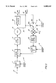
- FIG. 1 illustrates a standard Phase-Locked Loop (PLL) block diagram.
- the basic PLL has an input frequency f in 2 which is divided by a divider 4, wherein the divider 4 divides the input frequency f in 2 by a value N.
- the output of the divider 4 is then input into a phase detector 6.
- the phase detector 6 outputs a voltage that is proportional to a phase difference between two input frequencies.
- This phase detector output voltage is then input into a loop filter 8.
- the loop filter 8 smoothes the phase detector output voltage and determines the loop performance based upon selected loop filter values.
- the output of the loop filter 8 adjusts the voltage-controlled oscillator (VCO) 10 and determines the output frequency of the VCO 10.
- the output of the of the VCO 10 is then fed back as an input to the phase detector 6 via a feedback loop 14.
- the output voltage of the phase detector 6 will vary according to any change in the phase difference between the output frequency of the VCO 10 and the input frequency f in 2.
- the feedback loop 14 thus provides a means of "locking" the phase of the output frequency f out 12 in accordance with the phase of the input frequency f in 2. If the input frequency f in 2 is a highly stable reference frequency, the PLL circuit produces a highly stable output frequency f in 12. The PLL circuit produces an output frequency f out 12, equal to the value [f in / N], wherein the phase of the VCO output frequency f out 12 follows the phase of the input frequency f in 2.
- a divider 16 may be used in the feedback loop 14 in order to change the output frequency f out 12.
- the output frequency f out 12 from the VCO 10 is equal to the value [(f in * M)/N]. If the divider 16 is implemented using a programmable counter, the value of M can be changed. Thus, the output frequency f out 12 can be adjusted to a desired value by varying the value of "M.”
- a phase modulated intermediate input frequency (IF) 18 is input to the first divider 4 of the PLL circuit.
- the feedback loop 14 contains two additional blocks, however.
- a mixer 22 mixes a local oscillator signal RF LO 26 with the RF OUT signal 20 and the output of the mixer 22 is input into a bandpass (BP) filter 24.
- the output of the mixer may be referred to as the "feedback frequency.”
- the feedback frequency can be selected from one of the numerous frequencies produced by the harmonic mixing. In general, the output of the mixer is equal to [ ⁇ n*RF OUT ⁇ m*RF LO ].
- n and m are "1," then the selected outputs of the mixer are either RF out --RF LO or RF LO --RF OUT (assuming frequency down-conversion).
- the bandpass filter 24 removes any unwanted mixing products produced by the mixer 22 and determines which frequency is fed-back through the M divider 16. The operation of the remaining blocks operate as described in the previous figures.
- the PLL circuit translates i.e., moves) the frequency of the input IF 18 frequency to the VCO frequency with the same phase.
- a desired output frequency RF out 20 can be produced for a given intermediate frequency (IF) 18.
- f fb is the feedback frequency output by the mixer
- f VCO is the VCO frequency
- f in is the input frequency.
- the variables "n” and "m” are integer multipliers introuced by the harmonic mixing.
- a second PLL circuit For applications that require two different RF out frequency bands, such as a dual-band cellular telephone, a second PLL circuit would normally be required.
- the transmit frequency bands are 890 -915 MHz for the GSM band and 1710 -1785 MHz for the DCS 1800 band. This would require using two separate VCOs, which adds complexity and expense to the over-all system design.
- a frequency multiplier (or divider) is connected to the output of the VCO in a standard PLL circuit.
- the output of the VCO and the output of the frequency multiplier are selectably fed-back, depending upon which output frequency is desired.
- An output frequency may be taken directly from the VCO or the frequency multiplier.
- the output of the frequency multiplier is fed back and a control signal adjusts the gain of the phase detector and/or the loop filter in order to compensate for the loop gain caused by the frequency multiplier.
- Additional frequency multipliers or dividers may be added to provide for multi-band operation. However, the phase detector and/or loop filter gain must be adjusted accordingly to compensate for the loop gain of the circuit.
- the values of the N and M dividers are adjusted.
- a frequency multiplier (or divider) block is connected to the output of the VCO.
- the frequency multiplier multiplies the output of the VCO by a multiplier value "H.”
- the output of the multiplier is not fed-back, however. Additional multipliers can be added as desired, and a desired output selected via a control signal.
- the N divider value is adjusted by a control signal, such that when the output frequency is taken from the output of the frequency multiplier, the ratio N/M is set equal to the value "H.” This architecture keeps the modulation index equal at the input and the output of the loop.
- the M value, the N value, the phase detector gain and the loop filter gain may all be adjusted, in order to keep the N/M ratio equal to the multiplier "H" and to compensate for the loop gain caused by changing the value of M.
- the fourth embodiment is advantageous for design situations in which the third embodiment is inadequate to cover the desired frequency ranges.
- the N and M dividers can be made programmable to allow for easy adjustment of the N/M ratio and to allow for multi-band operation.
- FIG. 1 is a block diagram showing a basic Phase-Locked Loop (PLL);
- PLL Phase-Locked Loop
- FIG. 2 is a block diagram of a PLL frequency synthesizer utilizing a program counter in the feedback loop
- FIG. 3 is a block diagram of a PLL wherein the feedback loop contains a mixer
- FIG. 4 is a block diagram of a PLL according to a first embodiment of the present invention, wherein a frequency doubler and a band-switch are used to provide two different output frequency ranges;
- FIG. 5 is a block diagram of a PLL according to a second embodiment of the present invention:
- FIG. 6 is a block diagram of a PLL according to a third embodiment of the present invention, wherein multiplier blocks and a selector are incorporated outside of the feedback loop.
- FIG. 7 is a block diagram of a PLL according to a fourth embodiment of the present invention.
- VCO voltage-controlled oscillator
- the present invention will now be described with reference to FIG. 4.
- the PLL block diagram operates generally as described in FIG. 3.
- the present invention adds two additional components to the basic circuit, a frequency doubler 28 and a band-switch 38.
- the band-switch 38 is connected directly to the output of the VCO 10 (i.e. the band-switch 38 is in position "38a")
- the circuit operates as described above with reference to FIG. 3. That is, ##EQU2##
- the operation of the PLL circuit is quite different, however.
- the output of the frequency doubler 28 is fed back.
- the frequency doubler 28 doubles the input frequency supplied by the VCO 10 and outputs a frequency signal RF OUT1 30.
- the frequency doubler 28 could actually divide the VCO output frequency by 2, or could triple the frequency supplied by the VCO 10.
- the term "multiplier" as used herein encompasses a divider, since multiplying by 1/2 is equivalent to dividing by 2.
- the loop gain of the PLL circuit doubles, assuming that the M divider 16 value is kept constant. If the value of M was changed to compensate for the loop gain, the phase relationship between the input and output frequencies would also change. Thus, there is a need to compensate for the loop gain of the circuit when the band-switch 38 is connected to the frequency doubler 28 output.
- This problem may be solved by either having a loop filter 8 with a selectable gain, a phase detector 6 with a selectable gain, or by having both a loop filter 8 and a phase detector 6 with a selectable gain.
- a control signal line 40 is input to the band-switch 36, the phase detector 6 and/or the loop filter 8.
- the gain of the phase detector 6 and/or the loop filter 8 are set to the required values for taking the output directly from the VCO 10.
- the band-switch 38 is set to position "38b" by the control signal on the control signal line 40, the gain of the phase detector 6 and/or the loop filter 8 is set to the required value for taking the output from the frequency doubler 28.
- the VCO can be designed to output the frequency range 855-915 MHz. Taking the output frequency directly from the VCO provides the necessary frequency range for the GSM transmit band (890-915 MHz). Switching the band-switch 38 to position "38b" doubles the output frequency, and provides the frequencies of 1710-1785 MHz required for the DCS 1800 transmit band.
- FIG. 5 illustrates a second embodiment of the present invention.
- the M value is kept constant. However, the value of M may be adjusted in order to compensate for the loop gain. If M is adjusted, though, the value of N also must also be adjusted in order to output the desired frequency.
- a control signal on the control signal line 41 adjusts the values of N and M, as required. Additionally, the gain of the phase detector and/or loop filter may also be adjusted if necessary (not shown).
- a Phase Locked Loop (PLL) circuit has a modulated IF signal input as the reference input to the phase detector 6.
- PLL Phase Locked Loop
- a modulated signal can be generated which is equal to H * f c , wherein f c is the output frequency of the VCO.
- the N/M ratio must be equal to the multiplication factor "H” applied to the VCO output frequency. This design requirement keeps the modulation index (and the modulation bandwidth) equal at the input and output of the loop.
- the divider ratio N/M must equal H in order to preserve the modulation index.
- FIG. 6 a third embodiment of the present invention is shown.
- the output of the VCO 10 is fed back to the mixer 22, and loop operates as described with reference to FIG. 3.
- the output of the VCO 10 is also input to two multiplier blocks 46, 48, however.
- the multiplier blocks 46, 48 multiply the output of the VCO 10 by the values "H 1 ,” and "H 2 ".
- H 1 can be set equal to "1" and H 2 equal to "2”.
- the output is taken from the H 1 46 block, the GSM band (890-915 MHz) can be covered.
- the DCS1800 band (1710-1785 MHz) can be covered.
- a control signal line 54 controls an output selector 50 in order to output the desired frequency.
- the control signal line 54 also adjusts the value of N, according to which output frequency is selected, in order to keep the N/M ratio equal to the multiplier H. Notice that it is desirable to keep the M value constant, in order not to change the loop gain of the circuit. Therefore, it is preferable to adjust only the N value. However, it is not always possible to adjust only the N value and still cover the desired frequency ranges.
- FIG. 7 illustrates a fourth embodiment of the present invention. This embodiment is similar to the embodiment of FIG. 6, except that the value of M is adjustable, as well as the value of N. This allows for greater flexibility in designing the circuit to cover desired output frequency ranges. If the value of M is adjusted, however, the loop gain changes. Therefore, in order to compensate for the loop gain, the gain of the phase detector 6 and/or the loop filter 8 are also adjusted.
- the main advantage of this architecture over the prior art is that only one VCO is required in order to cover two (or more) frequency bands. Also, the mixer in the loop always has the same input frequency range, allowing the mixer to be optimized for a given application.
- the N and M dividers can be made programmable to allow for easy adjustment of the N/M ratio, and to allow for multi-band operation.
Abstract
Description
Claims (19)
Priority Applications (4)
| Application Number | Priority Date | Filing Date | Title |
|---|---|---|---|
| US09/044,281 US6005443A (en) | 1998-03-19 | 1998-03-19 | Phase locked loop frequency synthesizer for multi-band application |
| US09/163,798 US6150890A (en) | 1998-03-19 | 1998-09-30 | Dual band transmitter for a cellular phone comprising a PLL |
| EP99301888A EP0944172A3 (en) | 1998-03-19 | 1999-03-12 | Phase-locked loop for generating an output signal in two or more frequency ranges |
| CN99103026.5A CN1237042A (en) | 1998-03-19 | 1999-03-19 | Modulation technique for multi-band applications |
Applications Claiming Priority (1)
| Application Number | Priority Date | Filing Date | Title |
|---|---|---|---|
| US09/044,281 US6005443A (en) | 1998-03-19 | 1998-03-19 | Phase locked loop frequency synthesizer for multi-band application |
Related Child Applications (1)
| Application Number | Title | Priority Date | Filing Date |
|---|---|---|---|
| US09/163,798 Continuation-In-Part US6150890A (en) | 1998-03-19 | 1998-09-30 | Dual band transmitter for a cellular phone comprising a PLL |
Publications (1)
| Publication Number | Publication Date |
|---|---|
| US6005443A true US6005443A (en) | 1999-12-21 |
Family
ID=21931493
Family Applications (1)
| Application Number | Title | Priority Date | Filing Date |
|---|---|---|---|
| US09/044,281 Expired - Lifetime US6005443A (en) | 1998-03-19 | 1998-03-19 | Phase locked loop frequency synthesizer for multi-band application |
Country Status (3)
| Country | Link |
|---|---|
| US (1) | US6005443A (en) |
| EP (1) | EP0944172A3 (en) |
| CN (1) | CN1237042A (en) |
Cited By (25)
| Publication number | Priority date | Publication date | Assignee | Title |
|---|---|---|---|---|
| US6150890A (en) * | 1998-03-19 | 2000-11-21 | Conexant Systems, Inc. | Dual band transmitter for a cellular phone comprising a PLL |
| US6255912B1 (en) * | 1999-09-27 | 2001-07-03 | Conexant Systems, Inc. | Phase lock loop used as up converter and for reducing phase noise of an output signal |
| US6333679B1 (en) * | 1999-06-11 | 2001-12-25 | Telefonaktiebolaget Lm Ericsson (Publ) | Phase locked loop arrangement in which VCO frequency is a fraction of reference frequency |
| US6348823B1 (en) * | 1999-06-29 | 2002-02-19 | Industrial Technology Research Institute | Digital controlled oscillating circuit of digital phase lock loops |
| US20020090917A1 (en) * | 2001-01-10 | 2002-07-11 | Matsushita Electric Industrial Co., Ltd | Frequency synthesizer and method of generating frequency-divided signal |
| US6516184B1 (en) * | 1999-08-31 | 2003-02-04 | Skyworks Solutions, Inc. | Multi-band transceiver having multi-slot capability |
| US6636086B2 (en) * | 2000-12-08 | 2003-10-21 | Agilent Technologies, Inc. | High performance microwave synthesizer using multiple-modulator fractional-N divider |
| US7003274B1 (en) | 2003-03-05 | 2006-02-21 | Cisco Systems Wireless Networking (Australia) Pty Limited | Frequency synthesizer and synthesis method for generating a multiband local oscillator signal |
| US20060057992A1 (en) * | 2004-09-13 | 2006-03-16 | Broadcom Corporation | Frequency allocation using a single VCO |
| US20070155024A1 (en) * | 2003-02-28 | 2007-07-05 | Peter Miethe | Method and device for selectively detecting ferromagnetic or superparamagnetic particles. |
| US7356111B1 (en) * | 2003-01-14 | 2008-04-08 | Advanced Micro Devices, Inc. | Apparatus and method for fractional frequency division using multi-phase output VCO |
| US20090066425A1 (en) * | 2007-09-11 | 2009-03-12 | Samsung Electro-Mechnics Co., Ltd. | Frequency synthesizer having multi-band voltage controlled oscillator |
| US7696797B1 (en) * | 2005-03-31 | 2010-04-13 | Schnaitter William N | Signal generator with output frequency greater than the oscillator frequency |
| US20110102090A1 (en) * | 2009-10-30 | 2011-05-05 | MStar Semiconductor , Inc. | Phase Locked Loop and Method Thereof |
| US8014477B1 (en) * | 2006-03-08 | 2011-09-06 | Marvell International Ltd. | Receiver employing selectable A/D sample clock frequency |
| CN102324929A (en) * | 2011-04-22 | 2012-01-18 | 中国科学院上海微系统与信息技术研究所 | Hopping frequency synthesizer for front end of millimeter wave holographic imaging system |
| CN104702273A (en) * | 2015-03-25 | 2015-06-10 | 西安华芯半导体有限公司 | Delay phase locked loop for preventing error locking and phase locking method thereof |
| CN104702272A (en) * | 2015-03-25 | 2015-06-10 | 西安华芯半导体有限公司 | Delay phase-locked circuit and method for automatically adjusting initial delay of delay phase-locked loop |
| CN104702277A (en) * | 2013-12-10 | 2015-06-10 | 展讯通信(上海)有限公司 | Phase-locked loop circuit |
| US20150303929A1 (en) * | 2012-11-29 | 2015-10-22 | Nanowave Technologies Inc. | Low spurious synthesizer circuit and method |
| US9553596B1 (en) | 2015-12-24 | 2017-01-24 | Industrial Technology Research Institute | Frequency synthesizer and method for frequency synthesis |
| CN109521834A (en) * | 2018-10-31 | 2019-03-26 | 武汉精立电子技术有限公司 | A kind of DP signal generation device and method |
| CN110460330A (en) * | 2019-08-20 | 2019-11-15 | 四川九洲电器集团有限责任公司 | A kind of packaging technology and frequency source of frequency source |
| US10566982B1 (en) * | 2016-11-14 | 2020-02-18 | Marvell International Ltd. | Systems and methods for suppressing oscillator-induced spurs in frequency synthesizers |
| US20220239301A1 (en) * | 2021-01-28 | 2022-07-28 | Anritsu Company | Frequency synthesizers having low phase noise |
Families Citing this family (15)
| Publication number | Priority date | Publication date | Assignee | Title |
|---|---|---|---|---|
| KR100785003B1 (en) * | 2002-09-06 | 2007-12-11 | 삼성전자주식회사 | Multiband transceiver using control voltage of phase locked loop, and method therefor |
| KR100471156B1 (en) * | 2002-12-03 | 2005-03-10 | 삼성전기주식회사 | Device for generating wide tunable frequency using frequency division |
| JP2007515083A (en) * | 2003-09-05 | 2007-06-07 | フレクストロニクス デザイン フィンランド オサケ ユキチュア | Method for steering an oscillator and oscillator |
| DE102004023220A1 (en) * | 2004-03-11 | 2005-10-06 | Siemens Ag | Method and apparatus for generating a variable frequency vibration |
| US7821350B2 (en) * | 2007-01-19 | 2010-10-26 | Qualcomm Incorporated | Methods and apparatus for dynamic frequency scaling of phase locked loops for microprocessors |
| US7948290B2 (en) * | 2007-07-23 | 2011-05-24 | Panasonic Corporation | Digital PLL device |
| WO2011149657A1 (en) * | 2010-05-28 | 2011-12-01 | Marvell World Trade Ltd. | Method and apparatus for drift compensation in pll |
| DE102011110781A1 (en) * | 2010-08-22 | 2012-03-08 | Krohne Messtechnik Gmbh | Circuit arrangement for generating high-frequency output signals forming a broadband frequency ramp |
| FR2992073B1 (en) * | 2012-06-19 | 2014-07-11 | Commissariat Energie Atomique | DEVICE FOR SUPPLYING AN ELECTRONIC CIRCUIT |
| US9276622B2 (en) * | 2013-03-14 | 2016-03-01 | Qualcomm Incorporated | Local oscillator (LO) generator with multi-phase divider and phase locked loop |
| CN103236841B (en) * | 2013-04-15 | 2016-06-15 | 北京大学 | Based on period ratio compared with switching regulator phase frequency detector and digital phase-locked loop |
| US9467156B2 (en) * | 2014-12-02 | 2016-10-11 | Mediatek Inc. | Frequency synthesizing module and related frequency gain determining method |
| CN105306080B (en) * | 2015-11-30 | 2017-08-25 | 上海航天测控通信研究所 | A kind of spaceborne phase-locked receive of X frequency ranges |
| CN105897298A (en) * | 2016-06-03 | 2016-08-24 | 北京航空航天大学 | Multi-stage modular wireless transceiver experimental platform |
| CN110729996B (en) * | 2019-11-12 | 2023-05-26 | 中电科思仪科技股份有限公司 | Miniaturized phase-locked loop circuit and method for twice phase locking |
Citations (2)
| Publication number | Priority date | Publication date | Assignee | Title |
|---|---|---|---|---|
| US3854102A (en) * | 1973-08-09 | 1974-12-10 | Itt | Multiple frequency band frequency synthesizer |
| US3882424A (en) * | 1972-12-29 | 1975-05-06 | Int Standard Electric Corp | Phase locked loop transmitter |
Family Cites Families (4)
| Publication number | Priority date | Publication date | Assignee | Title |
|---|---|---|---|---|
| GB1314462A (en) * | 1970-04-28 | 1973-04-26 | Sperry Rand Corp | Signal generators |
| JPS5344110A (en) * | 1976-10-05 | 1978-04-20 | Saibanetsuto Kougiyou Kk | System for synchronizing and synthesizing frequency of radio transmitter*receiver |
| FI112133B (en) * | 1996-03-29 | 2003-10-31 | Nokia Corp | Method of forming the frequencies of a direct conversion transmitter / receiver operating in two different frequency ranges and a direct conversion transmitter / receiver of a radio communication system operating in two different frequency ranges and using the foregoing in a mobile telephone |
| SE519263C2 (en) * | 1996-12-02 | 2003-02-04 | Ericsson Telefon Ab L M | Device for transmitting at multiple frequencies in a radio communication system |
-
1998
- 1998-03-19 US US09/044,281 patent/US6005443A/en not_active Expired - Lifetime
-
1999
- 1999-03-12 EP EP99301888A patent/EP0944172A3/en not_active Withdrawn
- 1999-03-19 CN CN99103026.5A patent/CN1237042A/en active Pending
Patent Citations (2)
| Publication number | Priority date | Publication date | Assignee | Title |
|---|---|---|---|---|
| US3882424A (en) * | 1972-12-29 | 1975-05-06 | Int Standard Electric Corp | Phase locked loop transmitter |
| US3854102A (en) * | 1973-08-09 | 1974-12-10 | Itt | Multiple frequency band frequency synthesizer |
Cited By (40)
| Publication number | Priority date | Publication date | Assignee | Title |
|---|---|---|---|---|
| US6150890A (en) * | 1998-03-19 | 2000-11-21 | Conexant Systems, Inc. | Dual band transmitter for a cellular phone comprising a PLL |
| US6333679B1 (en) * | 1999-06-11 | 2001-12-25 | Telefonaktiebolaget Lm Ericsson (Publ) | Phase locked loop arrangement in which VCO frequency is a fraction of reference frequency |
| US6348823B1 (en) * | 1999-06-29 | 2002-02-19 | Industrial Technology Research Institute | Digital controlled oscillating circuit of digital phase lock loops |
| US6516184B1 (en) * | 1999-08-31 | 2003-02-04 | Skyworks Solutions, Inc. | Multi-band transceiver having multi-slot capability |
| US6255912B1 (en) * | 1999-09-27 | 2001-07-03 | Conexant Systems, Inc. | Phase lock loop used as up converter and for reducing phase noise of an output signal |
| US6636086B2 (en) * | 2000-12-08 | 2003-10-21 | Agilent Technologies, Inc. | High performance microwave synthesizer using multiple-modulator fractional-N divider |
| US20020090917A1 (en) * | 2001-01-10 | 2002-07-11 | Matsushita Electric Industrial Co., Ltd | Frequency synthesizer and method of generating frequency-divided signal |
| US7356111B1 (en) * | 2003-01-14 | 2008-04-08 | Advanced Micro Devices, Inc. | Apparatus and method for fractional frequency division using multi-phase output VCO |
| US20070155024A1 (en) * | 2003-02-28 | 2007-07-05 | Peter Miethe | Method and device for selectively detecting ferromagnetic or superparamagnetic particles. |
| US8071027B2 (en) * | 2003-02-28 | 2011-12-06 | Forschungszentrum Juelich Gmbh | Method and device for selectively detecting ferromagnetic or superparamagnetic particles |
| US7515931B2 (en) | 2003-03-05 | 2009-04-07 | Cisco Technology, Inc. | Frequency synthesizer and synthesis method for generating a multiband local oscillator signal |
| US7003274B1 (en) | 2003-03-05 | 2006-02-21 | Cisco Systems Wireless Networking (Australia) Pty Limited | Frequency synthesizer and synthesis method for generating a multiband local oscillator signal |
| US20060094374A1 (en) * | 2003-03-05 | 2006-05-04 | Olip John A P | Frequency synthesizer and synthesis method for generating a multiband local oscillator signal |
| US7379722B2 (en) * | 2004-09-13 | 2008-05-27 | Broadcom Corporation | Frequency allocation using a single VCO |
| US20060057992A1 (en) * | 2004-09-13 | 2006-03-16 | Broadcom Corporation | Frequency allocation using a single VCO |
| US7696797B1 (en) * | 2005-03-31 | 2010-04-13 | Schnaitter William N | Signal generator with output frequency greater than the oscillator frequency |
| US8508262B2 (en) | 2005-03-31 | 2013-08-13 | William N. Schnaitter | Signal generator with output frequency greater than the oscillator frequency |
| US8014477B1 (en) * | 2006-03-08 | 2011-09-06 | Marvell International Ltd. | Receiver employing selectable A/D sample clock frequency |
| US8842787B1 (en) | 2006-03-08 | 2014-09-23 | Marvell International Ltd. | Receiver employing selectable A/D sample clock frequency |
| US8462887B1 (en) | 2006-03-08 | 2013-06-11 | Marvell International Ltd. | Receiver employing selectable A/D sample clock frequency |
| US20090066425A1 (en) * | 2007-09-11 | 2009-03-12 | Samsung Electro-Mechnics Co., Ltd. | Frequency synthesizer having multi-band voltage controlled oscillator |
| US7834705B2 (en) | 2007-09-11 | 2010-11-16 | Samsung Electro-Mechanics Co., Ltd. | Frequency synthesizer having multi-band voltage controlled oscillator |
| US20110102090A1 (en) * | 2009-10-30 | 2011-05-05 | MStar Semiconductor , Inc. | Phase Locked Loop and Method Thereof |
| US8258878B2 (en) * | 2009-10-30 | 2012-09-04 | Mstar Semiconductor, Inc. | Phase locked loop and method thereof |
| TWI419474B (en) * | 2009-10-30 | 2013-12-11 | Mstar Semiconductor Inc | Phase-locked loop and method thereof |
| CN102324929A (en) * | 2011-04-22 | 2012-01-18 | 中国科学院上海微系统与信息技术研究所 | Hopping frequency synthesizer for front end of millimeter wave holographic imaging system |
| US20150303929A1 (en) * | 2012-11-29 | 2015-10-22 | Nanowave Technologies Inc. | Low spurious synthesizer circuit and method |
| US9509322B2 (en) * | 2012-11-29 | 2016-11-29 | Nanowave Technologies Inc. | Low spurious synthesizer circuit and method |
| CN104702277A (en) * | 2013-12-10 | 2015-06-10 | 展讯通信(上海)有限公司 | Phase-locked loop circuit |
| CN104702272B (en) * | 2015-03-25 | 2017-12-29 | 西安紫光国芯半导体有限公司 | The delay phase lock circuitry and method of a kind of adjust automatically delay phase-locked loop initial delay |
| CN104702272A (en) * | 2015-03-25 | 2015-06-10 | 西安华芯半导体有限公司 | Delay phase-locked circuit and method for automatically adjusting initial delay of delay phase-locked loop |
| CN104702273A (en) * | 2015-03-25 | 2015-06-10 | 西安华芯半导体有限公司 | Delay phase locked loop for preventing error locking and phase locking method thereof |
| CN104702273B (en) * | 2015-03-25 | 2018-05-08 | 西安紫光国芯半导体有限公司 | It is a kind of to prevent the wrong delay phase-locked loop and its phase-lock technique locked |
| US9553596B1 (en) | 2015-12-24 | 2017-01-24 | Industrial Technology Research Institute | Frequency synthesizer and method for frequency synthesis |
| US10566982B1 (en) * | 2016-11-14 | 2020-02-18 | Marvell International Ltd. | Systems and methods for suppressing oscillator-induced spurs in frequency synthesizers |
| CN109521834A (en) * | 2018-10-31 | 2019-03-26 | 武汉精立电子技术有限公司 | A kind of DP signal generation device and method |
| CN109521834B (en) * | 2018-10-31 | 2021-04-06 | 武汉精立电子技术有限公司 | DP signal generating device and method |
| CN110460330A (en) * | 2019-08-20 | 2019-11-15 | 四川九洲电器集团有限责任公司 | A kind of packaging technology and frequency source of frequency source |
| US20220239301A1 (en) * | 2021-01-28 | 2022-07-28 | Anritsu Company | Frequency synthesizers having low phase noise |
| US11817871B2 (en) * | 2021-01-28 | 2023-11-14 | Anritsu Company | Frequency synthesizers having low phase noise |
Also Published As
| Publication number | Publication date |
|---|---|
| EP0944172A2 (en) | 1999-09-22 |
| CN1237042A (en) | 1999-12-01 |
| EP0944172A3 (en) | 2000-03-29 |
Similar Documents
| Publication | Publication Date | Title |
|---|---|---|
| US6005443A (en) | Phase locked loop frequency synthesizer for multi-band application | |
| US5259007A (en) | Phase locked loop frequency synthesizer | |
| US6150890A (en) | Dual band transmitter for a cellular phone comprising a PLL | |
| US5146186A (en) | Programmable-step, high-resolution frequency synthesizer which substantially eliminates spurious frequencies without adversely affecting phase noise | |
| US5034703A (en) | Frequency synthesizer | |
| EP1320189B1 (en) | Multi-band frequency synthesiser for mobile terminals | |
| US5152005A (en) | High resolution frequency synthesis | |
| US8502575B2 (en) | Fractional-N PLL using multiple phase comparison frequencies to improve spurious signal performance | |
| US6026307A (en) | Arrangement in a communication system | |
| US4627099A (en) | Communication apparatus for transmitting and receiving signals on different frequency bands | |
| US7579916B1 (en) | Low noise frequency synthesizer | |
| EP0244571B1 (en) | Low phase noise rf synthesizer | |
| EP0565362B1 (en) | Frequency tuning with synthesizer | |
| JPH0946225A (en) | Microwave/mullimeter wave band phase locked loop oscillation circuit | |
| WO2001024375A1 (en) | Phase locked loop frequency generating circuit and a receiver using the circuit | |
| US20020090917A1 (en) | Frequency synthesizer and method of generating frequency-divided signal | |
| GB2024546A (en) | Frequency Synthesisers | |
| US20020055344A1 (en) | Radio-frequency receiver | |
| EP1204201B1 (en) | Apparatus and method for producing an RF transmision signal | |
| AU642027B2 (en) | Multiloop microwave frequency synthesizer with low phase noise | |
| GB2130827A (en) | Frequency synthesizer | |
| JP2563256B2 (en) | Microwave frequency synthesizer | |
| US20040027205A1 (en) | Local oscillator apparatus for low-noise generation of arbitrary frequencies | |
| JPS6238351Y2 (en) | ||
| KR200152277Y1 (en) | Programmable filter. |
Legal Events
| Date | Code | Title | Description |
|---|---|---|---|
| AS | Assignment |
Owner name: ROCKWELL SEMICONDUCTOR SYSTEMS, INC., CALIFORNIA Free format text: ASSIGNMENT OF ASSIGNORS INTEREST;ASSIGNORS:DAMGAARD, MORTEN;LI, LEO;REEL/FRAME:009091/0873 Effective date: 19980306 |
|
| AS | Assignment |
Owner name: CREDIT SUISSE FIRST BOSTON, NEW YORK Free format text: SECURITY INTEREST;ASSIGNORS:CONEXANT SYSTEMS, INC.;BROOKTREE CORPORATION;BROOKTREE WORLDWIDE SALES CORPORATION;AND OTHERS;REEL/FRAME:009826/0056 Effective date: 19981221 |
|
| AS | Assignment |
Owner name: CONEXANT SYSTEMS, INC., CALIFORNIA Free format text: CHANGE OF NAME;ASSIGNOR:ROCKWELL SEMICONDUCTOR SYSTEMS, INC.;REEL/FRAME:010253/0107 Effective date: 19981014 |
|
| STCF | Information on status: patent grant |
Free format text: PATENTED CASE |
|
| AS | Assignment |
Owner name: CONEXANT SYSTEMS, INC., CALIFORNIA Free format text: RELEASE BY SECURED PARTY;ASSIGNOR:CREDIT SUISSE FIRST BOSTON;REEL/FRAME:012273/0217 Effective date: 20011018 Owner name: BROOKTREE WORLDWIDE SALES CORPORATION, CALIFORNIA Free format text: RELEASE BY SECURED PARTY;ASSIGNOR:CREDIT SUISSE FIRST BOSTON;REEL/FRAME:012273/0217 Effective date: 20011018 Owner name: BROOKTREE CORPORATION, CALIFORNIA Free format text: RELEASE BY SECURED PARTY;ASSIGNOR:CREDIT SUISSE FIRST BOSTON;REEL/FRAME:012273/0217 Effective date: 20011018 Owner name: CONEXANT SYSTEMS WORLDWIDE, INC., CALIFORNIA Free format text: RELEASE BY SECURED PARTY;ASSIGNOR:CREDIT SUISSE FIRST BOSTON;REEL/FRAME:012273/0217 Effective date: 20011018 |
|
| AS | Assignment |
Owner name: CONEXANT SYSTEMS, INC., CALIFORNIA Free format text: SECURITY INTEREST;ASSIGNOR:ALPHA INDUSTRIES, INC.;REEL/FRAME:013240/0860 Effective date: 20020625 |
|
| FEPP | Fee payment procedure |
Free format text: PAYOR NUMBER ASSIGNED (ORIGINAL EVENT CODE: ASPN); ENTITY STATUS OF PATENT OWNER: LARGE ENTITY |
|
| FPAY | Fee payment |
Year of fee payment: 4 |
|
| AS | Assignment |
Owner name: ALPHA INDUSTRIES, INC., MASSACHUSETTS Free format text: RELEASE AND RECONVEYANCE/SECURITY INTEREST;ASSIGNOR:CONEXANT SYSTEMS, INC.;REEL/FRAME:014580/0880 Effective date: 20030307 |
|
| AS | Assignment |
Owner name: SKYWORKS SOLUTIONS, INC., CALIFORNIA Free format text: ASSIGNMENT OF ASSIGNORS INTEREST;ASSIGNOR:CONEXANT SYSTEMS, INC.;REEL/FRAME:016784/0938 Effective date: 20020625 |
|
| FPAY | Fee payment |
Year of fee payment: 8 |
|
| FEPP | Fee payment procedure |
Free format text: PAYER NUMBER DE-ASSIGNED (ORIGINAL EVENT CODE: RMPN); ENTITY STATUS OF PATENT OWNER: LARGE ENTITY Free format text: PAYOR NUMBER ASSIGNED (ORIGINAL EVENT CODE: ASPN); ENTITY STATUS OF PATENT OWNER: LARGE ENTITY |
|
| AS | Assignment |
Owner name: WASHINGTON SUB, INC., CALIFORNIA Free format text: ASSIGNMENT OF ASSIGNORS INTEREST;ASSIGNOR:CONEXANT SYSTEMS, INC.;REEL/FRAME:026227/0673 Effective date: 20020625 |
|
| AS | Assignment |
Owner name: ALPHA INDUSTRIES, INC., MASSACHUSETTS Free format text: MERGER;ASSIGNOR:WASHINGTON SUB, INC.;REEL/FRAME:026231/0807 Effective date: 20020625 |
|
| AS | Assignment |
Owner name: SKYWORKS SOLUTIONS, INC., MASSACHUSETTS Free format text: MERGER;ASSIGNOR:ALPHA INDUSTRIES, INC.;REEL/FRAME:026235/0984 Effective date: 20020625 |
|
| FPAY | Fee payment |
Year of fee payment: 12 |
|
| FEPP | Fee payment procedure |
Free format text: PAYER NUMBER DE-ASSIGNED (ORIGINAL EVENT CODE: RMPN); ENTITY STATUS OF PATENT OWNER: LARGE ENTITY Free format text: PAYOR NUMBER ASSIGNED (ORIGINAL EVENT CODE: ASPN); ENTITY STATUS OF PATENT OWNER: LARGE ENTITY |
|
| AS | Assignment |
Owner name: INTEL CORPORATION, CALIFORNIA Free format text: ASSIGNMENT OF ASSIGNORS INTEREST;ASSIGNOR:SKYWORKS SOLUTIONS, INC.;REEL/FRAME:027674/0768 Effective date: 20110328 |