US6028339A - Dual work function CMOS device - Google Patents
Dual work function CMOS device Download PDFInfo
- Publication number
- US6028339A US6028339A US09/211,565 US21156598A US6028339A US 6028339 A US6028339 A US 6028339A US 21156598 A US21156598 A US 21156598A US 6028339 A US6028339 A US 6028339A
- Authority
- US
- United States
- Prior art keywords
- layer
- glass
- gate
- doped
- gates
- Prior art date
- Legal status (The legal status is an assumption and is not a legal conclusion. Google has not performed a legal analysis and makes no representation as to the accuracy of the status listed.)
- Expired - Lifetime
Links
Images


Classifications
-
- H—ELECTRICITY
- H01—ELECTRIC ELEMENTS
- H01L—SEMICONDUCTOR DEVICES NOT COVERED BY CLASS H10
- H01L21/00—Processes or apparatus adapted for the manufacture or treatment of semiconductor or solid state devices or of parts thereof
- H01L21/70—Manufacture or treatment of devices consisting of a plurality of solid state components formed in or on a common substrate or of parts thereof; Manufacture of integrated circuit devices or of parts thereof
- H01L21/77—Manufacture or treatment of devices consisting of a plurality of solid state components or integrated circuits formed in, or on, a common substrate
- H01L21/78—Manufacture or treatment of devices consisting of a plurality of solid state components or integrated circuits formed in, or on, a common substrate with subsequent division of the substrate into plural individual devices
- H01L21/82—Manufacture or treatment of devices consisting of a plurality of solid state components or integrated circuits formed in, or on, a common substrate with subsequent division of the substrate into plural individual devices to produce devices, e.g. integrated circuits, each consisting of a plurality of components
- H01L21/822—Manufacture or treatment of devices consisting of a plurality of solid state components or integrated circuits formed in, or on, a common substrate with subsequent division of the substrate into plural individual devices to produce devices, e.g. integrated circuits, each consisting of a plurality of components the substrate being a semiconductor, using silicon technology
- H01L21/8232—Field-effect technology
- H01L21/8234—MIS technology, i.e. integration processes of field effect transistors of the conductor-insulator-semiconductor type
- H01L21/8238—Complementary field-effect transistors, e.g. CMOS
- H01L21/823828—Complementary field-effect transistors, e.g. CMOS with a particular manufacturing method of the gate conductors, e.g. particular materials, shapes
- H01L21/823842—Complementary field-effect transistors, e.g. CMOS with a particular manufacturing method of the gate conductors, e.g. particular materials, shapes gate conductors with different gate conductor materials or different gate conductor implants, e.g. dual gate structures
-
- Y—GENERAL TAGGING OF NEW TECHNOLOGICAL DEVELOPMENTS; GENERAL TAGGING OF CROSS-SECTIONAL TECHNOLOGIES SPANNING OVER SEVERAL SECTIONS OF THE IPC; TECHNICAL SUBJECTS COVERED BY FORMER USPC CROSS-REFERENCE ART COLLECTIONS [XRACs] AND DIGESTS
- Y10—TECHNICAL SUBJECTS COVERED BY FORMER USPC
- Y10S—TECHNICAL SUBJECTS COVERED BY FORMER USPC CROSS-REFERENCE ART COLLECTIONS [XRACs] AND DIGESTS
- Y10S257/00—Active solid-state devices, e.g. transistors, solid-state diodes
- Y10S257/90—MOSFET type gate sidewall insulating spacer
Definitions
- This invention relates generally to a method of manufacturing integrated circuit (IC) chips and the IC chips produced thereby. More specifically, the present invention relates to a dual work function complementary metal oxide semiconductor (CMOS) device and a method for producing these devices.
- CMOS complementary metal oxide semiconductor
- Another feature of the present invention is that the need for a layer of photoresist and the associated masking and processing steps are obviated. By eliminating the second photoresist step, alignment problems are not multiplied and throughput time is reduced.
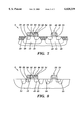
- FIG. 1 is a schematic of a first step in the process of the present invention
- FIG. 3 is a schematic of a third step in the process of the present invention.
- FIG. 8 is a second alternative schematic of the final product of the present invention.
- FIGS. 1-6 there is shown a stepwise series of schematic views of the process and integrated circuit (IC) chip 8 of preferred embodiments of the present invention.
- a cross section of the IC chip 8 is shown in FIG. 1.
- the chip 8 itself is typically a P+ substrate, in which isolation areas may have been formed, either shallow trench isolation areas 10 or semi-recessed oxide isolation (S-ROX) structures. Between these areas, active areas are formed.
- the active areas commonly include n-wells 12, p-wells 14, or the doped substrate itself.
- the well structures 12,14 are implanted in the usual fashion and then a gate oxide 16 is grown on the surface. On top of gate oxide layer 16, an undoped polysilicon 18 layer is deposited to form the structure shown in FIG. 1.
- gates 20, 22 are defined using the conventional method, which comprises depositing a layer of a photosensitive material, known as a resist, exposing the photosensitive material to an energy source, e.g., e-beams, i-line or deep ultraviolet light, or X-rays, thereby changing the solubility of the resist so that it is either more soluble in the energy struck regions (positive resist) or less soluble in the areas the light strikes (negative resist), developing the resist, which basically comprises rinsing off the more-soluble areas, and subjecting the entire surface to a reactive ion etch process in which the areas that are not protected by a layer of resist material are etched away.
- this entire “expose, develop, etch” process will be referred to as "defining" an area.
- the resist material is then removed and the resulting structure is shown in FIG. 2.
- Gates, 20, 22, are on the substrate surface over the active areas.
- spacers 24, 26 may optionally be formed.
- the spacer material is deposited as a layer of an insulative material, either a nitride or an oxide depending on the device, and anisotropically reactive ion etched on the entire surface until the horizontal portions have been etched away, leaving the areas that are on the sidewalls of gates 20 and 22 to form spacers 24, 26.
- first layer 30, containing a first type of impurity is deposited over the entire surface.
- the first type of impurity may either be an n-type or a p-type impurity.
- the material is commonly either a phosphosilicate glass (PSG) or an arsenic silicate glass (ASG).
- PSG phosphosilicate glass
- ASG arsenic silicate glass
- the arsenic doped glass is used in place of the phosphorus doped glass because it may offer advantages, such as differences in diffusivity.
- first layer 30 contains a p-type impurity the material is commonly borosilicate glass (BSG).
- first layer 30 is BSG, i.e., a p-doped silicate glass.
- a nitride layer 32 or other protective layer may then be deposited on the surface of first layer 30 to prevent diffusion of subsequent dopants through this first layer. If nitride layer 32 is not used, the thickness of first layer 30 must be controlled to prevent the diffusion of subsequent dopants through first layer 30. However, in such an embodiment, the bulk of first layer 30 may cause complications in the patterning of the device.
- the first layer 30 is then defined, by blocking the P-channel devices with the photoresist and performing a wet etch using buffered hydrofluoric acid (BHF) to remove the BSG from the N-channel devices.
- BHF buffered hydrofluoric acid
- the layer would be defined so that the glass (PSG or ASG) would remain on the areas to be doped with the n-type impurity.
- the resist is then stripped off, the surface prepared for the next step by a reduced etch in hydrofluoric acid (HF) solution, and a second layer 34 having a second impurity is deposited on the surface, as shown in FIG. 4.
- Second layer 34 similar to first layer 30 and protective layer 32, is a conformal coating over the entire surface.
- a first source 40 and a first drain 42 having p-type impurities are formed in the n-well 12.
- a second source 46 and a second drain 44 having n-type impurities are formed in the p-well 14.
- a source and drain form a junction so that there is one junction for each well and defined gate. This is preferably performed for a sub-0.1 micron(gm) scale device by heating the entire structure to a temperature in the range of about 850° Celsius (C) to about 1100° C. for approximately 10 seconds (sec.) in a rapid thermal anneal (RTA) tool.
- RTA rapid thermal anneal
- the amount of time necessary and the optimal temperature will vary depending on the device to be fabricated and the corresponding structure needed. For example, if the anneal is performed for a longer time and/or at a higher temperature, the dopant will be driven deeper into the material below and will have a more gradual concentration gradient. Conversely, as the time and/or temperature of the anneal process (DT) is reduced, the overlap of the gate is varied. In this CMOS process, the need for a spacer to define diffusion overlap is optional. In general, the DT process provides ample process window for diffusion overlap.
- Gate electrode 36 is degeneratively doped either P+ or N+ due to the rapid movement of dopant in a polycrystalline structure.
- the gate electrode thickness (which ultimately governs its geometric control) is now not limited by the penetration of high energy implants and can be scaled to sub-0.1 ⁇ m.
- gate electrodes 36 are scaled in height to the junction heights. As shown in FIGS. 6 and 7, gate electrode height 52 is substantially similar to junction height 50.
- the optimal height for gate electrode is in the range of about 500 to about 1500 angstroms.
- junctions are scaled narrowly (e.g. 100 angstroms)
- the contacts which are etched may penetrate into the silicon. The result of this is damage through the junction, commonly referred to as spiking.
- a deeper junction can be implanted for contact.
- a second set of junctions comprised of sources 54 and 58 and drains 48 and 56 have been implanted deeper into the IC chip than the first set of junctions.
- first layer 20, protective layer 32, and second layer 34 are allowed to remain along the sidewalls of gate 20, whereas second layer 34 is allowed to remain as a spacer along the sidewalls of gate 22.
- first layer 20, protective layer 32, and second layer 34 are allowed to remain along the sidewalls of gate 20
- second layer 34 is allowed to remain as a spacer along the sidewalls of gate 22.
- protective layer 32 and second layer 34 can be removed from gate 20 leaving only first layer 30 as a spacer.
- spun on glass may be substituted for either or both of the BSG and PSG or ASG films.
- Doped SOG is commercially available with either boron, phosphorus, or arsenic and may be utilized if it is necessary or desirable because of other design and technology constraints.
- dislocations are dramatically reduced or completely eliminated, because the step which typically causes dislocations, namely the high dose ion implantation step, has been replaced by a solid source diffusion step. Additionally, the gate poly and the source-drain regions of a given device are simultaneously doped with the same dopant without additional masks or costs.
Abstract
Description
Claims (16)
Priority Applications (1)
| Application Number | Priority Date | Filing Date | Title |
|---|---|---|---|
| US09/211,565 US6028339A (en) | 1996-08-29 | 1998-12-14 | Dual work function CMOS device |
Applications Claiming Priority (3)
| Application Number | Priority Date | Filing Date | Title |
|---|---|---|---|
| US08/705,579 US5770490A (en) | 1996-08-29 | 1996-08-29 | Method for producing dual work function CMOS device |
| US96399697A | 1997-11-04 | 1997-11-04 | |
| US09/211,565 US6028339A (en) | 1996-08-29 | 1998-12-14 | Dual work function CMOS device |
Related Parent Applications (1)
| Application Number | Title | Priority Date | Filing Date |
|---|---|---|---|
| US96399697A Continuation-In-Part | 1996-08-29 | 1997-11-04 |
Publications (1)
| Publication Number | Publication Date |
|---|---|
| US6028339A true US6028339A (en) | 2000-02-22 |
Family
ID=27107533
Family Applications (1)
| Application Number | Title | Priority Date | Filing Date |
|---|---|---|---|
| US09/211,565 Expired - Lifetime US6028339A (en) | 1996-08-29 | 1998-12-14 | Dual work function CMOS device |
Country Status (1)
| Country | Link |
|---|---|
| US (1) | US6028339A (en) |
Cited By (28)
| Publication number | Priority date | Publication date | Assignee | Title |
|---|---|---|---|---|
| US6255152B1 (en) * | 1999-10-01 | 2001-07-03 | United Microelectronics Corp. | Method of fabricating CMOS using Si-B layer to form source/drain extension junction |
| US6362034B1 (en) * | 1999-12-20 | 2002-03-26 | Intel Corporation | Method of forming MOSFET gate electrodes having reduced depletion region growth sensitivity to applied electric field |
| US6373111B1 (en) * | 1999-11-30 | 2002-04-16 | Intel Corporation | Work function tuning for MOSFET gate electrodes |
| US6448618B1 (en) * | 1997-02-27 | 2002-09-10 | Kabushiki Kaisha Toshiba | Semiconductor device and method for manufacturing the same |
| US6492217B1 (en) * | 1998-06-30 | 2002-12-10 | Intel Corporation | Complementary metal gates and a process for implementation |
| US6512273B1 (en) * | 2000-01-28 | 2003-01-28 | Advanced Micro Devices, Inc. | Method and structure for improving hot carrier immunity for devices with very shallow junctions |
| US6518106B2 (en) * | 2001-05-26 | 2003-02-11 | Motorola, Inc. | Semiconductor device and a method therefor |
| US6586808B1 (en) | 2002-06-06 | 2003-07-01 | Advanced Micro Devices, Inc. | Semiconductor device having multi-work function gate electrode and multi-segment gate dielectric |
| US6630720B1 (en) | 2001-12-26 | 2003-10-07 | Advanced Micro Devices, Inc. | Asymmetric semiconductor device having dual work function gate and method of fabrication |
| KR100405963B1 (en) * | 2001-06-27 | 2003-11-14 | 상록코리아 (주) | Method of operating minimun channel memory device |
| US6686612B1 (en) | 2002-10-01 | 2004-02-03 | T-Ram, Inc. | Thyristor-based device adapted to inhibit parasitic current |
| US6690039B1 (en) | 2002-10-01 | 2004-02-10 | T-Ram, Inc. | Thyristor-based device that inhibits undesirable conductive channel formation |
| US6693333B1 (en) | 2001-05-01 | 2004-02-17 | Advanced Micro Devices, Inc. | Semiconductor-on-insulator circuit with multiple work functions |
| US20040075111A1 (en) * | 2002-05-31 | 2004-04-22 | Dureseti Chidambarrao | High performance logic and high density embedded dram with borderless contact and antispacer |
| US20040075119A1 (en) * | 2002-10-08 | 2004-04-22 | Sanjay Natarajan | Forming polysilicon structures |
| US20040113211A1 (en) * | 2001-10-02 | 2004-06-17 | Steven Hung | Gate electrode with depletion suppression and tunable workfunction |
| US6806584B2 (en) * | 2002-10-21 | 2004-10-19 | International Business Machines Corporation | Semiconductor device structure including multiple fets having different spacer widths |
| US20040224451A1 (en) * | 2003-05-08 | 2004-11-11 | International Business Machines Corporation | Dual gate material process for cmos technologies |
| US20040262784A1 (en) * | 2003-06-30 | 2004-12-30 | International Business Machines Corporation | High performance cmos device structures and method of manufacture |
| US20050072986A1 (en) * | 2001-09-03 | 2005-04-07 | Nec Corporation | Group-III nitride semiconductor device |
| KR100482745B1 (en) * | 2000-12-29 | 2005-04-14 | 주식회사 하이닉스반도체 | Method of manufacturing a transistor in a semiconductor device |
| US20060186490A1 (en) * | 2003-11-28 | 2006-08-24 | International Business Machines Corporation | Metal carbide gate structure and method of fabrication |
| US7129148B2 (en) * | 2000-08-15 | 2006-10-31 | Seiko Epson Corporation | Methods for manufacturing semiconductor devices and semiconductor devices having trench isolation regions |
| US20080128771A1 (en) * | 2006-12-05 | 2008-06-05 | International Business Machines Corporation | Nano-fuse structural arrangements having blow protection barrier spaced from and surrounding fuse link |
| US20090130831A1 (en) * | 2007-11-16 | 2009-05-21 | Ji-Hwan Park | Semiconductor device and method of fabricating the same |
| US9269633B2 (en) | 2000-12-18 | 2016-02-23 | The Board Of Trustees Of The Leland Stanford Junior University | Method for forming gate electrode with depletion suppression and tunable workfunction |
| US9401311B2 (en) | 2014-05-02 | 2016-07-26 | International Business Machines Corporation | Self aligned structure and method for high-K metal gate work function tuning |
| US9514995B1 (en) | 2015-05-21 | 2016-12-06 | Globalfoundries Inc. | Implant-free punch through doping layer formation for bulk FinFET structures |
Citations (18)
| Publication number | Priority date | Publication date | Assignee | Title |
|---|---|---|---|---|
| JPS58197072A (en) * | 1982-05-12 | 1983-11-16 | Shinko Electric Co Ltd | Thermal printer |
| JPS60197072A (en) * | 1984-03-21 | 1985-10-05 | Hitachi Ltd | Coding processing method of color picture information |
| JPS63104325A (en) * | 1986-10-21 | 1988-05-09 | Ricoh Co Ltd | Manufacture of c-mos semiconductor device |
| US4755478A (en) * | 1987-08-13 | 1988-07-05 | International Business Machines Corporation | Method of forming metal-strapped polysilicon gate electrode for FET device |
| JPH02188914A (en) * | 1989-01-17 | 1990-07-25 | Seiko Instr Inc | Manufacture of semiconductor device |
| JPH02188913A (en) * | 1989-01-17 | 1990-07-25 | Seiko Instr Inc | Manufacture of semiconductor device |
| US5024960A (en) * | 1987-06-16 | 1991-06-18 | Texas Instruments Incorporated | Dual LDD submicron CMOS process for making low and high voltage transistors with common gate |
| JPH0492416A (en) * | 1990-08-07 | 1992-03-25 | Seiko Epson Corp | Manufacture of semiconductor device |
| US5190888A (en) * | 1990-10-23 | 1993-03-02 | Siemens Aktiengesellschaft | Method for producing a doped polycide layer on a semiconductor substrate |
| US5234850A (en) * | 1990-09-04 | 1993-08-10 | Industrial Technology Research Institute | Method of fabricating a nitride capped MOSFET for integrated circuits |
| US5254866A (en) * | 1990-04-03 | 1993-10-19 | Mitsubishi Denki Kabushiki Kaisha | LDD CMOS with wider oxide sidewall on PMOS than NMOS |
| US5258645A (en) * | 1990-03-09 | 1993-11-02 | Fujitsu Limited | Semiconductor device having MOS transistor and a sidewall with a double insulator layer structure |
| US5274261A (en) * | 1990-07-31 | 1993-12-28 | Texas Instruments Incorporated | Integrated circuit degradation resistant structure |
| US5329138A (en) * | 1991-07-29 | 1994-07-12 | Hitachi, Ltd. | Short channel CMOS device capable of high performance at low voltage |
| US5465000A (en) * | 1992-03-20 | 1995-11-07 | Siliconix Incorporated | Threshold adjustment in vertical DMOS devices |
| US5464789A (en) * | 1989-06-08 | 1995-11-07 | Kabushiki Kaisha Toshiba | Method of manufacturing a CMOS semiconductor device |
| US5468986A (en) * | 1993-05-31 | 1995-11-21 | Kabushiki Kaisha Toshiba | Semiconductor static random access memory device with covered driver transistors |
| US5729056A (en) * | 1995-12-15 | 1998-03-17 | Vanguard International Semiconductor Corporation | Low cycle time CMOS process |
-
1998
- 1998-12-14 US US09/211,565 patent/US6028339A/en not_active Expired - Lifetime
Patent Citations (19)
| Publication number | Priority date | Publication date | Assignee | Title |
|---|---|---|---|---|
| JPS58197072A (en) * | 1982-05-12 | 1983-11-16 | Shinko Electric Co Ltd | Thermal printer |
| JPS60197072A (en) * | 1984-03-21 | 1985-10-05 | Hitachi Ltd | Coding processing method of color picture information |
| JPS63104325A (en) * | 1986-10-21 | 1988-05-09 | Ricoh Co Ltd | Manufacture of c-mos semiconductor device |
| US5024960A (en) * | 1987-06-16 | 1991-06-18 | Texas Instruments Incorporated | Dual LDD submicron CMOS process for making low and high voltage transistors with common gate |
| US4755478A (en) * | 1987-08-13 | 1988-07-05 | International Business Machines Corporation | Method of forming metal-strapped polysilicon gate electrode for FET device |
| JPH02188914A (en) * | 1989-01-17 | 1990-07-25 | Seiko Instr Inc | Manufacture of semiconductor device |
| JPH02188913A (en) * | 1989-01-17 | 1990-07-25 | Seiko Instr Inc | Manufacture of semiconductor device |
| US5464789A (en) * | 1989-06-08 | 1995-11-07 | Kabushiki Kaisha Toshiba | Method of manufacturing a CMOS semiconductor device |
| US5258645A (en) * | 1990-03-09 | 1993-11-02 | Fujitsu Limited | Semiconductor device having MOS transistor and a sidewall with a double insulator layer structure |
| US5254866A (en) * | 1990-04-03 | 1993-10-19 | Mitsubishi Denki Kabushiki Kaisha | LDD CMOS with wider oxide sidewall on PMOS than NMOS |
| US5274261A (en) * | 1990-07-31 | 1993-12-28 | Texas Instruments Incorporated | Integrated circuit degradation resistant structure |
| JPH0492416A (en) * | 1990-08-07 | 1992-03-25 | Seiko Epson Corp | Manufacture of semiconductor device |
| US5234850A (en) * | 1990-09-04 | 1993-08-10 | Industrial Technology Research Institute | Method of fabricating a nitride capped MOSFET for integrated circuits |
| US5324974A (en) * | 1990-09-04 | 1994-06-28 | Industrial Technology Research Institute | Nitride capped MOSFET for integrated circuits |
| US5190888A (en) * | 1990-10-23 | 1993-03-02 | Siemens Aktiengesellschaft | Method for producing a doped polycide layer on a semiconductor substrate |
| US5329138A (en) * | 1991-07-29 | 1994-07-12 | Hitachi, Ltd. | Short channel CMOS device capable of high performance at low voltage |
| US5465000A (en) * | 1992-03-20 | 1995-11-07 | Siliconix Incorporated | Threshold adjustment in vertical DMOS devices |
| US5468986A (en) * | 1993-05-31 | 1995-11-21 | Kabushiki Kaisha Toshiba | Semiconductor static random access memory device with covered driver transistors |
| US5729056A (en) * | 1995-12-15 | 1998-03-17 | Vanguard International Semiconductor Corporation | Low cycle time CMOS process |
Non-Patent Citations (8)
| Title |
|---|
| BU889 0198 Low Reistivity Stack for Dual Doped Polysilicon Gate Electrode Jun. 1991. No. 326 Kenneth Mason Publications Ltd., England. * |
| BU889-0198\Low Reistivity Stack for Dual Doped Polysilicon Gate Electrode\Jun. 1991. No. 326\Kenneth Mason Publications Ltd., England. |
| Dialog 1996 Derwent Info, Ltd. Mar. 1996 p. 2 JP 6283725. * |
| Dialog 1996 Derwent Info, Ltd.\Mar. 1996\p. 2\JP 6283725. |
| IBM Technical Disclosure Bulletin vo. 26 No. 10A Mar. 1984 Oxidizable P Channel Gate Electrode. * |
| IBM Technical Disclosure Bulletin vol. 31 No. 7 Dec. 1988 Dual Work Function Doping. * |
| IBM Technical Disclosure Bulletin\vo. 26 No. 10A\Mar. 1984\Oxidizable P-Channel Gate Electrode. |
| IBM Technical Disclosure Bulletin\vol. 31 No. 7\Dec. 1988\Dual Work Function Doping. |
Cited By (42)
| Publication number | Priority date | Publication date | Assignee | Title |
|---|---|---|---|---|
| US6448618B1 (en) * | 1997-02-27 | 2002-09-10 | Kabushiki Kaisha Toshiba | Semiconductor device and method for manufacturing the same |
| US6492217B1 (en) * | 1998-06-30 | 2002-12-10 | Intel Corporation | Complementary metal gates and a process for implementation |
| US6255152B1 (en) * | 1999-10-01 | 2001-07-03 | United Microelectronics Corp. | Method of fabricating CMOS using Si-B layer to form source/drain extension junction |
| US20030151074A1 (en) * | 1999-11-30 | 2003-08-14 | Jun-Fei Zheng | Work function tuning for mosfet gate electrodes |
| US6696333B1 (en) | 1999-11-30 | 2004-02-24 | Intel Corporation | Method of making integrated circuit with MOSFETs having bi-layer metal gate electrodes |
| US6794232B2 (en) | 1999-11-30 | 2004-09-21 | Intel Corporation | Method of making MOSFET gate electrodes with tuned work function |
| US6373111B1 (en) * | 1999-11-30 | 2002-04-16 | Intel Corporation | Work function tuning for MOSFET gate electrodes |
| US6790731B2 (en) * | 1999-11-30 | 2004-09-14 | Intel Corporation | Method for tuning a work function for MOSFET gate electrodes |
| US20040065903A1 (en) * | 1999-11-30 | 2004-04-08 | Intel Corporation | Integrated circuit with MOSFETS having bi-layer metal gate electordes and method of making same |
| US6879009B2 (en) | 1999-11-30 | 2005-04-12 | Intel Corporation | Integrated circuit with MOSFETS having bi-layer metal gate electrodes |
| US6362034B1 (en) * | 1999-12-20 | 2002-03-26 | Intel Corporation | Method of forming MOSFET gate electrodes having reduced depletion region growth sensitivity to applied electric field |
| US6512273B1 (en) * | 2000-01-28 | 2003-01-28 | Advanced Micro Devices, Inc. | Method and structure for improving hot carrier immunity for devices with very shallow junctions |
| US7129148B2 (en) * | 2000-08-15 | 2006-10-31 | Seiko Epson Corporation | Methods for manufacturing semiconductor devices and semiconductor devices having trench isolation regions |
| US9269633B2 (en) | 2000-12-18 | 2016-02-23 | The Board Of Trustees Of The Leland Stanford Junior University | Method for forming gate electrode with depletion suppression and tunable workfunction |
| KR100482745B1 (en) * | 2000-12-29 | 2005-04-14 | 주식회사 하이닉스반도체 | Method of manufacturing a transistor in a semiconductor device |
| US6693333B1 (en) | 2001-05-01 | 2004-02-17 | Advanced Micro Devices, Inc. | Semiconductor-on-insulator circuit with multiple work functions |
| US6518106B2 (en) * | 2001-05-26 | 2003-02-11 | Motorola, Inc. | Semiconductor device and a method therefor |
| KR100405963B1 (en) * | 2001-06-27 | 2003-11-14 | 상록코리아 (주) | Method of operating minimun channel memory device |
| US7760785B2 (en) * | 2001-09-03 | 2010-07-20 | Nec Corporation | Group-III nitride semiconductor device |
| US20050072986A1 (en) * | 2001-09-03 | 2005-04-07 | Nec Corporation | Group-III nitride semiconductor device |
| US20040113211A1 (en) * | 2001-10-02 | 2004-06-17 | Steven Hung | Gate electrode with depletion suppression and tunable workfunction |
| US6630720B1 (en) | 2001-12-26 | 2003-10-07 | Advanced Micro Devices, Inc. | Asymmetric semiconductor device having dual work function gate and method of fabrication |
| US6873010B2 (en) | 2002-05-31 | 2005-03-29 | International Business Machines Corporation | High performance logic and high density embedded dram with borderless contact and antispacer |
| US20040075111A1 (en) * | 2002-05-31 | 2004-04-22 | Dureseti Chidambarrao | High performance logic and high density embedded dram with borderless contact and antispacer |
| US6586808B1 (en) | 2002-06-06 | 2003-07-01 | Advanced Micro Devices, Inc. | Semiconductor device having multi-work function gate electrode and multi-segment gate dielectric |
| US6690039B1 (en) | 2002-10-01 | 2004-02-10 | T-Ram, Inc. | Thyristor-based device that inhibits undesirable conductive channel formation |
| US6686612B1 (en) | 2002-10-01 | 2004-02-03 | T-Ram, Inc. | Thyristor-based device adapted to inhibit parasitic current |
| US20040075119A1 (en) * | 2002-10-08 | 2004-04-22 | Sanjay Natarajan | Forming polysilicon structures |
| US6806584B2 (en) * | 2002-10-21 | 2004-10-19 | International Business Machines Corporation | Semiconductor device structure including multiple fets having different spacer widths |
| US20040224451A1 (en) * | 2003-05-08 | 2004-11-11 | International Business Machines Corporation | Dual gate material process for cmos technologies |
| US20080026522A1 (en) * | 2003-06-30 | 2008-01-31 | International Business Machines Corporation | High performance cmos device structures and method of manufacture |
| US20040262784A1 (en) * | 2003-06-30 | 2004-12-30 | International Business Machines Corporation | High performance cmos device structures and method of manufacture |
| US7436029B2 (en) | 2003-06-30 | 2008-10-14 | International Business Machines Corporation | High performance CMOS device structures and method of manufacture |
| US7279746B2 (en) * | 2003-06-30 | 2007-10-09 | International Business Machines Corporation | High performance CMOS device structures and method of manufacture |
| US7667278B2 (en) * | 2003-11-28 | 2010-02-23 | International Business Machines Corporation | Metal carbide gate structure and method of fabrication |
| US20060186490A1 (en) * | 2003-11-28 | 2006-08-24 | International Business Machines Corporation | Metal carbide gate structure and method of fabrication |
| US7867859B1 (en) | 2004-01-16 | 2011-01-11 | The Board Of Trustees Of The Leland Stanford Junior University | Gate electrode with depletion suppression and tunable workfunction |
| US20080128771A1 (en) * | 2006-12-05 | 2008-06-05 | International Business Machines Corporation | Nano-fuse structural arrangements having blow protection barrier spaced from and surrounding fuse link |
| US7777296B2 (en) | 2006-12-05 | 2010-08-17 | International Business Machines Corporation | Nano-fuse structural arrangements having blow protection barrier spaced from and surrounding fuse link |
| US20090130831A1 (en) * | 2007-11-16 | 2009-05-21 | Ji-Hwan Park | Semiconductor device and method of fabricating the same |
| US9401311B2 (en) | 2014-05-02 | 2016-07-26 | International Business Machines Corporation | Self aligned structure and method for high-K metal gate work function tuning |
| US9514995B1 (en) | 2015-05-21 | 2016-12-06 | Globalfoundries Inc. | Implant-free punch through doping layer formation for bulk FinFET structures |
Similar Documents
| Publication | Publication Date | Title |
|---|---|---|
| US5770490A (en) | Method for producing dual work function CMOS device | |
| US6028339A (en) | Dual work function CMOS device | |
| US6747326B2 (en) | Low voltage high performance semiconductor device having punch through prevention implants | |
| EP0387999B1 (en) | Process for forming high-voltage and low-voltage CMOS transistors on a single integrated circuit chip | |
| US5989966A (en) | Method and a deep sub-micron field effect transistor structure for suppressing short channel effects | |
| US4902640A (en) | High speed double polycide bipolar/CMOS integrated circuit process | |
| US4578128A (en) | Process for forming retrograde dopant distributions utilizing simultaneous outdiffusion of dopants | |
| US4435896A (en) | Method for fabricating complementary field effect transistor devices | |
| US5780898A (en) | Semiconductor device with a vertical field effect transistor and method of manufacturing the same | |
| US5489546A (en) | Method of forming CMOS devices using independent thickness spacers in a split-polysilicon DRAM process | |
| US6316318B1 (en) | Angled implant to build MOS transistors in contact holes | |
| US5986328A (en) | Buried contact architecture | |
| US5877050A (en) | Method of making N-channel and P-channel devices using two tube anneals and two rapid thermal anneals | |
| US20060281302A1 (en) | Semiconductor damascene trench and methods thereof | |
| US4488348A (en) | Method for making a self-aligned vertically stacked gate MOS device | |
| US5079177A (en) | Process for fabricating high performance bicmos circuits | |
| US5753548A (en) | Method for preventing fluorine outgassing-induced interlevel dielectric delamination on P-channel FETS | |
| US6207482B1 (en) | Integration method for deep sub-micron dual gate transistor design | |
| US4075754A (en) | Self aligned gate for di-CMOS | |
| US5898189A (en) | Integrated circuit including an oxide-isolated localized substrate and a standard silicon substrate and fabrication method | |
| US5320976A (en) | Method for manufacturing VLSI semiconductor device | |
| US6251744B1 (en) | Implant method to improve characteristics of high voltage isolation and high voltage breakdown | |
| US5707896A (en) | Method for preventing delamination of interlevel dielectric layer over FET P+ doped polysilicon gate electrodes on semiconductor integrated circuits | |
| US6333220B1 (en) | Method and apparatus for providing low-GIDL dual workfunction gate doping with borderless diffusion contact | |
| US5093707A (en) | Semiconductor device with bipolar and cmos transistors |
Legal Events
| Date | Code | Title | Description |
|---|---|---|---|
| AS | Assignment |
Owner name: INTERNATIONAL BUSINESS MACHINES CORPORATION, NEW Y Free format text: ASSIGNMENT OF ASSIGNORS INTEREST;ASSIGNORS:FRENETTE, ROBERT O.;HALLOCK, DALE P.;MONGEON, STEPHEN A.;AND OTHERS;REEL/FRAME:009661/0035;SIGNING DATES FROM 19981210 TO 19981214 |
|
| FEPP | Fee payment procedure |
Free format text: PAYOR NUMBER ASSIGNED (ORIGINAL EVENT CODE: ASPN); ENTITY STATUS OF PATENT OWNER: LARGE ENTITY |
|
| STCF | Information on status: patent grant |
Free format text: PATENTED CASE |
|
| FEPP | Fee payment procedure |
Free format text: PAYOR NUMBER ASSIGNED (ORIGINAL EVENT CODE: ASPN); ENTITY STATUS OF PATENT OWNER: LARGE ENTITY Free format text: PAYER NUMBER DE-ASSIGNED (ORIGINAL EVENT CODE: RMPN); ENTITY STATUS OF PATENT OWNER: LARGE ENTITY |
|
| FPAY | Fee payment |
Year of fee payment: 4 |
|
| FPAY | Fee payment |
Year of fee payment: 8 |
|
| FPAY | Fee payment |
Year of fee payment: 12 |