US6029882A - Plastic solder array using injection molded solder - Google Patents
Plastic solder array using injection molded solder Download PDFInfo
- Publication number
- US6029882A US6029882A US09/067,904 US6790498A US6029882A US 6029882 A US6029882 A US 6029882A US 6790498 A US6790498 A US 6790498A US 6029882 A US6029882 A US 6029882A
- Authority
- US
- United States
- Prior art keywords
- solder
- mold
- major surface
- substrate
- chamfered
- Prior art date
- Legal status (The legal status is an assumption and is not a legal conclusion. Google has not performed a legal analysis and makes no representation as to the accuracy of the status listed.)
- Expired - Fee Related
Links
Images

Classifications
-
- B—PERFORMING OPERATIONS; TRANSPORTING
- B23—MACHINE TOOLS; METAL-WORKING NOT OTHERWISE PROVIDED FOR
- B23K—SOLDERING OR UNSOLDERING; WELDING; CLADDING OR PLATING BY SOLDERING OR WELDING; CUTTING BY APPLYING HEAT LOCALLY, e.g. FLAME CUTTING; WORKING BY LASER BEAM
- B23K3/00—Tools, devices, or special appurtenances for soldering, e.g. brazing, or unsoldering, not specially adapted for particular methods
- B23K3/06—Solder feeding devices; Solder melting pans
- B23K3/0607—Solder feeding devices
- B23K3/0638—Solder feeding devices for viscous material feeding, e.g. solder paste feeding
-
- H—ELECTRICITY
- H01—ELECTRIC ELEMENTS
- H01L—SEMICONDUCTOR DEVICES NOT COVERED BY CLASS H10
- H01L21/00—Processes or apparatus adapted for the manufacture or treatment of semiconductor or solid state devices or of parts thereof
- H01L21/02—Manufacture or treatment of semiconductor devices or of parts thereof
- H01L21/04—Manufacture or treatment of semiconductor devices or of parts thereof the devices having at least one potential-jump barrier or surface barrier, e.g. PN junction, depletion layer or carrier concentration layer
- H01L21/48—Manufacture or treatment of parts, e.g. containers, prior to assembly of the devices, using processes not provided for in a single one of the subgroups H01L21/06 - H01L21/326
- H01L21/4814—Conductive parts
- H01L21/4846—Leads on or in insulating or insulated substrates, e.g. metallisation
- H01L21/4853—Connection or disconnection of other leads to or from a metallisation, e.g. pins, wires, bumps
-
- H—ELECTRICITY
- H05—ELECTRIC TECHNIQUES NOT OTHERWISE PROVIDED FOR
- H05K—PRINTED CIRCUITS; CASINGS OR CONSTRUCTIONAL DETAILS OF ELECTRIC APPARATUS; MANUFACTURE OF ASSEMBLAGES OF ELECTRICAL COMPONENTS
- H05K3/00—Apparatus or processes for manufacturing printed circuits
- H05K3/30—Assembling printed circuits with electric components, e.g. with resistor
- H05K3/32—Assembling printed circuits with electric components, e.g. with resistor electrically connecting electric components or wires to printed circuits
- H05K3/34—Assembling printed circuits with electric components, e.g. with resistor electrically connecting electric components or wires to printed circuits by soldering
- H05K3/3457—Solder materials or compositions; Methods of application thereof
- H05K3/3468—Applying molten solder
-
- B—PERFORMING OPERATIONS; TRANSPORTING
- B23—MACHINE TOOLS; METAL-WORKING NOT OTHERWISE PROVIDED FOR
- B23K—SOLDERING OR UNSOLDERING; WELDING; CLADDING OR PLATING BY SOLDERING OR WELDING; CUTTING BY APPLYING HEAT LOCALLY, e.g. FLAME CUTTING; WORKING BY LASER BEAM
- B23K2101/00—Articles made by soldering, welding or cutting
- B23K2101/36—Electric or electronic devices
- B23K2101/40—Semiconductor devices
-
- H—ELECTRICITY
- H01—ELECTRIC ELEMENTS
- H01L—SEMICONDUCTOR DEVICES NOT COVERED BY CLASS H10
- H01L2224/00—Indexing scheme for arrangements for connecting or disconnecting semiconductor or solid-state bodies and methods related thereto as covered by H01L24/00
- H01L2224/01—Means for bonding being attached to, or being formed on, the surface to be connected, e.g. chip-to-package, die-attach, "first-level" interconnects; Manufacturing methods related thereto
- H01L2224/10—Bump connectors; Manufacturing methods related thereto
- H01L2224/11—Manufacturing methods
- H01L2224/11001—Involving a temporary auxiliary member not forming part of the manufacturing apparatus, e.g. removable or sacrificial coating, film or substrate
- H01L2224/11003—Involving a temporary auxiliary member not forming part of the manufacturing apparatus, e.g. removable or sacrificial coating, film or substrate for holding or transferring the bump preform
-
- H—ELECTRICITY
- H01—ELECTRIC ELEMENTS
- H01L—SEMICONDUCTOR DEVICES NOT COVERED BY CLASS H10
- H01L2924/00—Indexing scheme for arrangements or methods for connecting or disconnecting semiconductor or solid-state bodies as covered by H01L24/00
- H01L2924/01—Chemical elements
- H01L2924/01019—Potassium [K]
-
- H—ELECTRICITY
- H01—ELECTRIC ELEMENTS
- H01L—SEMICONDUCTOR DEVICES NOT COVERED BY CLASS H10
- H01L2924/00—Indexing scheme for arrangements or methods for connecting or disconnecting semiconductor or solid-state bodies as covered by H01L24/00
- H01L2924/01—Chemical elements
- H01L2924/01068—Erbium [Er]
-
- H—ELECTRICITY
- H01—ELECTRIC ELEMENTS
- H01L—SEMICONDUCTOR DEVICES NOT COVERED BY CLASS H10
- H01L2924/00—Indexing scheme for arrangements or methods for connecting or disconnecting semiconductor or solid-state bodies as covered by H01L24/00
- H01L2924/013—Alloys
- H01L2924/0132—Binary Alloys
- H01L2924/01322—Eutectic Alloys, i.e. obtained by a liquid transforming into two solid phases
-
- H—ELECTRICITY
- H01—ELECTRIC ELEMENTS
- H01L—SEMICONDUCTOR DEVICES NOT COVERED BY CLASS H10
- H01L2924/00—Indexing scheme for arrangements or methods for connecting or disconnecting semiconductor or solid-state bodies as covered by H01L24/00
- H01L2924/10—Details of semiconductor or other solid state devices to be connected
- H01L2924/102—Material of the semiconductor or solid state bodies
- H01L2924/1025—Semiconducting materials
- H01L2924/10251—Elemental semiconductors, i.e. Group IV
- H01L2924/10253—Silicon [Si]
-
- H—ELECTRICITY
- H05—ELECTRIC TECHNIQUES NOT OTHERWISE PROVIDED FOR
- H05K—PRINTED CIRCUITS; CASINGS OR CONSTRUCTIONAL DETAILS OF ELECTRIC APPARATUS; MANUFACTURE OF ASSEMBLAGES OF ELECTRICAL COMPONENTS
- H05K2201/00—Indexing scheme relating to printed circuits covered by H05K1/00
- H05K2201/10—Details of components or other objects attached to or integrated in a printed circuit board
- H05K2201/10227—Other objects, e.g. metallic pieces
- H05K2201/10424—Frame holders
-
- H—ELECTRICITY
- H05—ELECTRIC TECHNIQUES NOT OTHERWISE PROVIDED FOR
- H05K—PRINTED CIRCUITS; CASINGS OR CONSTRUCTIONAL DETAILS OF ELECTRIC APPARATUS; MANUFACTURE OF ASSEMBLAGES OF ELECTRICAL COMPONENTS
- H05K2203/00—Indexing scheme relating to apparatus or processes for manufacturing printed circuits covered by H05K3/00
- H05K2203/01—Tools for processing; Objects used during processing
- H05K2203/0104—Tools for processing; Objects used during processing for patterning or coating
- H05K2203/0113—Female die used for patterning or transferring, e.g. temporary substrate having recessed pattern
-
- H—ELECTRICITY
- H05—ELECTRIC TECHNIQUES NOT OTHERWISE PROVIDED FOR
- H05K—PRINTED CIRCUITS; CASINGS OR CONSTRUCTIONAL DETAILS OF ELECTRIC APPARATUS; MANUFACTURE OF ASSEMBLAGES OF ELECTRICAL COMPONENTS
- H05K2203/00—Indexing scheme relating to apparatus or processes for manufacturing printed circuits covered by H05K3/00
- H05K2203/03—Metal processing
- H05K2203/0338—Transferring metal or conductive material other than a circuit pattern, e.g. bump, solder, printed component
-
- H—ELECTRICITY
- H05—ELECTRIC TECHNIQUES NOT OTHERWISE PROVIDED FOR
- H05K—PRINTED CIRCUITS; CASINGS OR CONSTRUCTIONAL DETAILS OF ELECTRIC APPARATUS; MANUFACTURE OF ASSEMBLAGES OF ELECTRICAL COMPONENTS
- H05K2203/00—Indexing scheme relating to apparatus or processes for manufacturing printed circuits covered by H05K3/00
- H05K2203/12—Using specific substances
- H05K2203/128—Molten metals, e.g. casting thereof, or melting by heating and excluding molten solder
Definitions
- This invention relates to the field of electronic packaging. More particularly, this invention relates to the packaging of integrated circuits (ICs) and mounting the ICs onto laminated printed circuit boards (PCBs) by means of solder balls using a technique known as plastic ball grid array (PBGA).
- ICs integrated circuits
- PCBs laminated printed circuit boards
- PBGA plastic ball grid array
- ICs comprise a complex assortment of microminiature electronic components on a silicon chip. To protect them from damage due to handling and moisture, ICs are typically housed in a ceramic or plastic package that is either soldered to a PCB or inserted into a matching socket which has been soldered into a printed circuit board.
- ceramic is the material favored in high reliability industrial and military applications; plastic, being less costly, is favored in commercial and consumer products. Many millions of these types of structures are manufactured every year, worldwide.
- FR4 resin laminate is becoming an industry norm because of its electrical, chemical and physical properties and its low cost.
- Means by which the IC package has been attached electronically to a PCB or another IC include metal pins in plastic pin grid array (PPGA), silk screened solder paste, solder preforms and solder balls. Injection molded techniques have been used in some cases to apply solder. In PBGA, solder balls are heated to a temperature at which it will reflow, and the solder is applied to contact pads on the PCB, also referred to herein as lands, electrically connecting the IC to the PCB. Some of the plastic packages have material sculpted out from the middle to form a recess in which the IC die will be placed when the plastic parts are laminated together.
- soldering processes may involve two reflow heating steps, the first reflow to attach solder at selected peripheral points on the surface of the laminate, and the second reflow to reshape the solder to a sphere.
- U.S. Pat. No. 4,585,157 to Stephen R. Belcher describes a method of bonding two IC chips face-to-face in a type of lead frame wire bonding called tape automated bonding (TAB).
- TAB tape automated bonding
- the patented method uses a tape bonding approach wherein the finger leads at a single site in a lead frame are divided into two groups and are bonded in two separate compression bonding processes. In the second bonding process, the first chip is flipped upside down and fit into a recess in a second thermode.
- the present invention is not directed to TAB, but rather is directed to a means and process of delivering discrete amounts of solder in PBGA to connection lands on a PCB having an IC mounted thereon.
- U.S. Pat. No. 5,979,664 to Alan M. Lyons et al describes a method of treating solder used in mounting an IC to a PC board in order to eliminate oxide at the solder surface without flux. To remove the oxide without flux, nitrogen or argon gas is flowed over the heated areas being joined. Unlike the present invention, the patent is not directed to the solder delivery itself, and in particular not directed to a solder injection mold delivery system and process.
- U.S. Pat. No. 5,551,148 to Kazui et al describes a flexible film having tapered through-holes filled with solder, which is heated and transferred under pressure from the larger diameter end of the through holes to a circuit board as bumps on pads. The transfer of solder is no good if the pressure is too low. At that point the flexible film is removed either by dissolving in hydrazine or ethylene diamine, sublimated by the heat of the soldering process, or peeled away.
- the solder injection mold of the present invention is not a flexible film, but a sturdy, reusable transfer device. Since it does not have to be dissolved, sublimated or peeled away, there is no handling of harsh chemicals or destruction or distortion of the injection mold used in the present invention.
- solder injection mold and process which is particularly suitable for supplying solder to a PBGA structure.
- Still another object of the invention is to provide a method of attaching solder balls to laminate carriers in a PBGA process with only one furnace reflow using IMS technology.
- an injection mold which includes on its second major surface a blind recess and at its first major surface a head, or reservoir, for delivery of molten solder to an array of through-holes in the mold which are double chamfered, i.e. fluted, with the wide ends facing outward at both ends of a through-hole which is shaped somewhat like an hour glass, a base plate for containing the molten solder within the through-holes until solder balls are formed and attached to a substrate, and a substrate for receiving the solder balls at their respective contact lands.
- molten solder flows into the upper chamfer, filling the through-hole, and is released from the lower chamfer to the contact land of the substrate as a solder ball during reflow.
- the combination of non-wettability of the mold material, the double chamfers and the aspect ratio of the mold through-holes permit the solder balls to form and release cleanly during reflow. Only one reflow step is required.
- the base plate and the injection mold can be made of the same material as the PCB substrate, or of a different non-wettable material having a substantially similar coefficient of thermal expansion (CTE).
- CTE coefficient of thermal expansion
- the non-wettability of the base plate material helps assure that the solder will form a ball and not stick to the base plate.
- the material of which the mold is made must be non-wettable so that the solder balls will form and adhere to the substrate without leaving solder residue within the walls of the mold through-holes. A clean mold can be reused easily.
- the mold material in the present invention has a life of about 10,000 usages and is compatible with the temperature of the molten eutectic solder.
- the CTE compatibility assures that solder balls in the mold through-holes will transfer to the PCB in the places desired, and that the mold material will not crack during solder transfer. It may be necessary to apply pressure between the mold and the substrate during reflow if, as a result of the material chosen, there is slight deviation from absolute flatness of these two parts with respect to each other at the temperature of the molten solder.
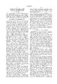
- FIG. 1A is a drawing, seen from the top, of the top piece of the PBGA mold, showing the through holes to be filled with solder.
- FIG. 1B is a drawing, seen from the bottom, of the top piece of the PBGA mold, showing the through holes to be filled with solder and a blind recess at the center.
- FIG. 2A is a cross-sectional side view showing the profile of a solder-filled through-holes of the PBGA mold prior to reflow;
- FIG. 2B is a cross-sectional side view showing the profile of a through-hole of the PBGA mold after reflow.
- FIG. 3 is a series of cross-sectional side view drawings showing 6 key steps in the PBGA injection molded soldering process.
- FIG. 1A is a view of the first major surface of PBGA injection mold 1 with first openings of through-holes 2 arranged in a peripheral array.
- the aspect ratio (depth: unchamfered width) of the hole is 1:1 or less, preferentially about 3:4 to about 1:2, a suitable width at center being about 0.035 inches.
- the solder is inserted into the mold at this end of through-holes 2 from a reservoir of molten solder, shown in FIG. 3 as feature 5, which is presented in more detail in U.S. Pat. No. 5,244,143.
- the temperature of the molten solder can be monitored in the reservoir for quality control.
- the mold is preferably comprised of graphite or FR4 resin laminate so that it has a (CTE) the same as, or substantially similar to, that of the PCB which is to receive the reflowed solder.
- CTE the same as, or substantially similar to, that of the PCB which is to receive the reflowed solder.
- Compatible CTEs will assure that the through holes containing the refiowed solder will attain alignment with the lands in the PCB that will receive the solder balls and that the mold itself will not crack at the heated solder temperature.
- FIG. 1B is a view of the second major surface of the PBGA injection mold 1 showing the second openings of mold through-holes 2, i.e. ends opposite to those seen in 1A. At the ends seen in FIG. 1B, solder balls 8 (not shown) will emerge after reflow and cooling to join to lands 10 on the substrate 6 (all shown in FIG. 2B).
- Blind recessed area 3 shown at the center of FIG. 1B is shaped to accommodate, with clearance, IC chip
- FIG. 2A is a cross sectional side view of PBGA injection mold 1 showing through-hole 2 filled with solder 9 before reflow.
- Through-hole 2 includes chamfers 12, shown also in FIG. 2B, at both ends to facilitate receiving solder 9 in molten form at a first end and to facilitate the release of solder ball 8 (shown in FIG. 2B) at a second end after reflow.
- FIG. 2B shows the solder ball 8 attached to contact land 10 on substrate 6 after reflow and prior to removal of mold 1.
- the solder 9 seen in FIG. 2A has retracted from the chamfered ends of the through-hole into the ball shape during reflow due to surface tension and has become attached to contact land 10 to which it is aligned.
- FIG. 3 illustrates the overall process of PGBA solder injection molding in six cross-sectional side views. Although the illustrations A-F do not show it, all through holes 2 are chamfered as shown in FIG. 2.
- FIG. 3A are seen the injection mold 1, the unfilled through holes 2, and the blind recess 3 to create overhead clearance for an IC chip 7 and any other components as seen in FIG. 3D.
- FIG. 3B are seen injection mold 1 in position atop a temporary base plate 4. Base plate 4 must be able to withstand exposure to the temperature of molten solder without distorting, reacting chemically or being wet by the molten solder.
- IMS head 5 which is filled with eutectic solder (63%:37% Sn:Pb, reflow @ 183 degrees C.), is slideably mounted on the mold and is seen in motion toward the left with respect to the mold, having filled six through-holes 2 with solder, indicated as darker through-holes 9.
- Other solder compositions may be used, provided the properties of the composition selected are compatible with, and nondestructive of, the other materials in the PBGA.
- FIG. 3C all through-holes 2 have been solder filled and the temporary base plate 4, which had been put in place in 3B to contain the molten solder 9 during filling of the through holes 2 from IMS head 5, has been removed, since the solder 9 is now solid within the chamfered through-holes 2.
- the substrate 6 may be treated with a small amount of flux, such as a water soluble flux or "no clean" flux, depending on whether the gaseous environment during transfer is oxidizing or not, e.g. whether it is air or nitrogen.
- Mold 1 is now ready to be lowered onto the top surface of a substrate 6, which has occurred in FIG. 3D.
- blind recess 3 is covering, with clearance, two chips 7 mounted on substrate 6, and the solder is positioned in through-holes 2 over the contact lands 10 (not shown), which will each receive a ball 8 of transferred solder upon reflow.
- FIG. 3E reflow has occurred.
Abstract
Disclosed is a solder injection mold apparatus and method for providing solder balls to a printed circuit board substrate using the solder injection mold apparatus in the plastic ball grid array (PBGA). The solder mold through holes are chamfered at entry and at exit ends to assist in receipt of molten solder and the formation and transfer of solder balls to lands on the substrate. A blind recess is provided in the second major surface of the mold, i.e. the side facing the substrate, in order to accommodate electronic components mounted thereon. Solder balls are delivered and metallurgically affixed to the lands in a process that requires only one reflow, leaving the through holes clean of solder and the mold ready for reuse. The material of which the substrate, mold and base plate are comprised is selected to be non-wettable by solder and mutually compatible with respect to CTE when exposed to temperatures of molten solder.
Description
This invention relates to the field of electronic packaging. More particularly, this invention relates to the packaging of integrated circuits (ICs) and mounting the ICs onto laminated printed circuit boards (PCBs) by means of solder balls using a technique known as plastic ball grid array (PBGA).
ICs comprise a complex assortment of microminiature electronic components on a silicon chip. To protect them from damage due to handling and moisture, ICs are typically housed in a ceramic or plastic package that is either soldered to a PCB or inserted into a matching socket which has been soldered into a printed circuit board. For IC housing, ceramic is the material favored in high reliability industrial and military applications; plastic, being less costly, is favored in commercial and consumer products. Many millions of these types of structures are manufactured every year, worldwide. For the PCB substrate, FR4 resin laminate is becoming an industry norm because of its electrical, chemical and physical properties and its low cost.
Means by which the IC package has been attached electronically to a PCB or another IC include metal pins in plastic pin grid array (PPGA), silk screened solder paste, solder preforms and solder balls. Injection molded techniques have been used in some cases to apply solder. In PBGA, solder balls are heated to a temperature at which it will reflow, and the solder is applied to contact pads on the PCB, also referred to herein as lands, electrically connecting the IC to the PCB. Some of the plastic packages have material sculpted out from the middle to form a recess in which the IC die will be placed when the plastic parts are laminated together. After the IC die is installed in the package, electrical connections are made to the die contact pads and to solder through the conductive metal patterns within the package. These soldering processes may involve two reflow heating steps, the first reflow to attach solder at selected peripheral points on the surface of the laminate, and the second reflow to reshape the solder to a sphere.
U.S. Pat. No. 4,585,157 to Stephen R. Belcher describes a method of bonding two IC chips face-to-face in a type of lead frame wire bonding called tape automated bonding (TAB). Rather than testing a chip at a site on the lead frame, the patented method uses a tape bonding approach wherein the finger leads at a single site in a lead frame are divided into two groups and are bonded in two separate compression bonding processes. In the second bonding process, the first chip is flipped upside down and fit into a recess in a second thermode. The present invention is not directed to TAB, but rather is directed to a means and process of delivering discrete amounts of solder in PBGA to connection lands on a PCB having an IC mounted thereon.
U.S. Pat. No. 5,979,664 to Alan M. Lyons et al describes a method of treating solder used in mounting an IC to a PC board in order to eliminate oxide at the solder surface without flux. To remove the oxide without flux, nitrogen or argon gas is flowed over the heated areas being joined. Unlike the present invention, the patent is not directed to the solder delivery itself, and in particular not directed to a solder injection mold delivery system and process.
U.S. Pat. No. 5,244,143 to Ference et al, assigned to the same assignee as the present invention, describes various embodiments of injection mold apparatus for solder. In the present invention, an injection mold apparatus for use with PBGA is described and a process set forth which is particularly adapted to PBGA. The patent is useful for its description of the solder reservoir.
U.S. Pat. No. 5,551,148 to Kazui et al describes a flexible film having tapered through-holes filled with solder, which is heated and transferred under pressure from the larger diameter end of the through holes to a circuit board as bumps on pads. The transfer of solder is no good if the pressure is too low. At that point the flexible film is removed either by dissolving in hydrazine or ethylene diamine, sublimated by the heat of the soldering process, or peeled away. The solder injection mold of the present invention is not a flexible film, but a sturdy, reusable transfer device. Since it does not have to be dissolved, sublimated or peeled away, there is no handling of harsh chemicals or destruction or distortion of the injection mold used in the present invention.
None of the above references addresses the problems, achieves the results or discloses the process and apparatus of the present invention.
Accordingly, it is an object of the invention to provide a solder injection mold and process which is particularly suitable for supplying solder to a PBGA structure.
It is a further object of the invention to provide a solder injection mold which will receive molten solder into a number of through-holes opening at a first major surface and dispense solder balls from those through-holes opening at a second major surface onto and in alignment with contact lands on the first major surface of a substrate, in particular onto a substrate having at least one electronic component mounted thereon, in a controlled and reliable fashion.
It is a further object of the invention to maintain the solder in place in the through holes within the mold through reflow and cooling of the molten solder into balls, and to then remove the mold from the substrate, leaving the solder balls behind and attached in ohmic contact to their respective lands on the substrate.
Still another object of the invention is to provide a method of attaching solder balls to laminate carriers in a PBGA process with only one furnace reflow using IMS technology.
It is also an object of the invention to avoid damage or destruction to any substrate, component, base plate or mold and to reuse the mold and base plate in the processing of a large number of substrates.
These and other objects are accomplished in the present invention using an injection mold which includes on its second major surface a blind recess and at its first major surface a head, or reservoir, for delivery of molten solder to an array of through-holes in the mold which are double chamfered, i.e. fluted, with the wide ends facing outward at both ends of a through-hole which is shaped somewhat like an hour glass, a base plate for containing the molten solder within the through-holes until solder balls are formed and attached to a substrate, and a substrate for receiving the solder balls at their respective contact lands.
Because of the uniqueness of the shape of the through-hole, molten solder flows into the upper chamfer, filling the through-hole, and is released from the lower chamfer to the contact land of the substrate as a solder ball during reflow. The combination of non-wettability of the mold material, the double chamfers and the aspect ratio of the mold through-holes permit the solder balls to form and release cleanly during reflow. Only one reflow step is required.
The base plate and the injection mold can be made of the same material as the PCB substrate, or of a different non-wettable material having a substantially similar coefficient of thermal expansion (CTE). The non-wettability of the base plate material helps assure that the solder will form a ball and not stick to the base plate. The material of which the mold is made must be non-wettable so that the solder balls will form and adhere to the substrate without leaving solder residue within the walls of the mold through-holes. A clean mold can be reused easily. The mold material in the present invention has a life of about 10,000 usages and is compatible with the temperature of the molten eutectic solder. The CTE compatibility assures that solder balls in the mold through-holes will transfer to the PCB in the places desired, and that the mold material will not crack during solder transfer. It may be necessary to apply pressure between the mold and the substrate during reflow if, as a result of the material chosen, there is slight deviation from absolute flatness of these two parts with respect to each other at the temperature of the molten solder.
FIG. 1A is a drawing, seen from the top, of the top piece of the PBGA mold, showing the through holes to be filled with solder.
FIG. 1B is a drawing, seen from the bottom, of the top piece of the PBGA mold, showing the through holes to be filled with solder and a blind recess at the center.
FIG. 2A is a cross-sectional side view showing the profile of a solder-filled through-holes of the PBGA mold prior to reflow;
FIG. 2B is a cross-sectional side view showing the profile of a through-hole of the PBGA mold after reflow.
FIG. 3 is a series of cross-sectional side view drawings showing 6 key steps in the PBGA injection molded soldering process.
In order to facilitate understanding of the present invention, reference is made to the following detailed description taken in conjunction with the drawings:
FIG. 1A is a view of the first major surface of PBGA injection mold 1 with first openings of through-holes 2 arranged in a peripheral array. The aspect ratio (depth: unchamfered width) of the hole is 1:1 or less, preferentially about 3:4 to about 1:2, a suitable width at center being about 0.035 inches. The solder is inserted into the mold at this end of through-holes 2 from a reservoir of molten solder, shown in FIG. 3 as feature 5, which is presented in more detail in U.S. Pat. No. 5,244,143. The temperature of the molten solder can be monitored in the reservoir for quality control. The mold is preferably comprised of graphite or FR4 resin laminate so that it has a (CTE) the same as, or substantially similar to, that of the PCB which is to receive the reflowed solder. Compatible CTEs will assure that the through holes containing the refiowed solder will attain alignment with the lands in the PCB that will receive the solder balls and that the mold itself will not crack at the heated solder temperature. FIG. 1B is a view of the second major surface of the PBGA injection mold 1 showing the second openings of mold through-holes 2, i.e. ends opposite to those seen in 1A. At the ends seen in FIG. 1B, solder balls 8 (not shown) will emerge after reflow and cooling to join to lands 10 on the substrate 6 (all shown in FIG. 2B). Blind recessed area 3 shown at the center of FIG. 1B is shaped to accommodate, with clearance, IC chip 7 (shown in FIG. 3E) mounted on PCB substrate 6 during solder transfer from the injection mold 1 to the PCB lands 10.
FIG. 2A is a cross sectional side view of PBGA injection mold 1 showing through-hole 2 filled with solder 9 before reflow. Through-hole 2 includes chamfers 12, shown also in FIG. 2B, at both ends to facilitate receiving solder 9 in molten form at a first end and to facilitate the release of solder ball 8 (shown in FIG. 2B) at a second end after reflow. FIG. 2B shows the solder ball 8 attached to contact land 10 on substrate 6 after reflow and prior to removal of mold 1. In FIG. 2B, the solder 9 seen in FIG. 2A has retracted from the chamfered ends of the through-hole into the ball shape during reflow due to surface tension and has become attached to contact land 10 to which it is aligned.
FIG. 3 illustrates the overall process of PGBA solder injection molding in six cross-sectional side views. Although the illustrations A-F do not show it, all through holes 2 are chamfered as shown in FIG. 2. In FIG. 3A are seen the injection mold 1, the unfilled through holes 2, and the blind recess 3 to create overhead clearance for an IC chip 7 and any other components as seen in FIG. 3D. In FIG. 3B are seen injection mold 1 in position atop a temporary base plate 4. Base plate 4 must be able to withstand exposure to the temperature of molten solder without distorting, reacting chemically or being wet by the molten solder. IMS head 5, which is filled with eutectic solder (63%:37% Sn:Pb, reflow @ 183 degrees C.), is slideably mounted on the mold and is seen in motion toward the left with respect to the mold, having filled six through-holes 2 with solder, indicated as darker through-holes 9. Other solder compositions may be used, provided the properties of the composition selected are compatible with, and nondestructive of, the other materials in the PBGA. In FIG. 3C all through-holes 2 have been solder filled and the temporary base plate 4, which had been put in place in 3B to contain the molten solder 9 during filling of the through holes 2 from IMS head 5, has been removed, since the solder 9 is now solid within the chamfered through-holes 2. The substrate 6 may be treated with a small amount of flux, such as a water soluble flux or "no clean" flux, depending on whether the gaseous environment during transfer is oxidizing or not, e.g. whether it is air or nitrogen. Mold 1 is now ready to be lowered onto the top surface of a substrate 6, which has occurred in FIG. 3D. In the FIG. 3D example, blind recess 3 is covering, with clearance, two chips 7 mounted on substrate 6, and the solder is positioned in through-holes 2 over the contact lands 10 (not shown), which will each receive a ball 8 of transferred solder upon reflow. In FIG. 3E reflow has occurred. Because of the non-wettability of the material selected for the mold 1 and the chamfers 12 (not shown), surface tension of the molten solder 9 acts to contract the solder into a ball shape 8. During reflow, a metallurgical bond is formed between the solder ball 8 and the substrate land 10 (not shown). Therefore when cooling has occurred, the mold 1 can be lifted away without disturbing the bonded solder balls 8, leaving behind an array of solder balls 8 soldered to their respective lands 10 (not shown) in the completed PBGA substrate in FIG. 3F. If there will be a slight distortion of the substrate 6 and the mold 1 with respect to each other due to the solder temperature, pressure can be applied after alignment during reflow, i.e. between 3D and 3E. While the invention has been described in conjunction with specific noniimiting embodiments, many modifications will be apparent to those skilled in the art in light of the foregoing information. Accordingly, it is intended that the present invention embrace all such modifications as fall within the spirit and broad scope of the appended claims.
Claims (8)
1. A method for forming solder balls on a substrate, comprising the steps of:
providing a solder injection mold having a first and a second major surface and at least one double chamfered through-hole extending therethrough, a first chamfered through hole opening at the first major surface of the mold for receiving molten solder from a solder reservoir and a second chamfered opening at the second major surface to transfer the solder to a substrate;
providing a blind recess in the second major surface of the mold, sufficient to clear any component mounted on a first major surface of a substrate;
applying a base plate at the second major surface of the mold to prevent release of molten solder;
filling from the solder reservoir molten solder into the at least one through-hole in the solder mold, allowing the solder to cool, and removing the base plate;
providing a substrate having a first major surface and a second major surface, the first major surface of which is provided with at least one mounted component for positioning within the blind recess of the mold and at least one contact land to receive the solder transferred from the second chamfered opening;
aligning the second chamfered opening in contact with the contact land;
reflowing the solder whereby the solder contracts into a spherical shape and attaches to the contact land; and
removing the mold.
2. The method set forth in claim 1, wherein the step of providing a solder injection mold having a first and a second major surface comprises providing a solder injection mold having a first and a second major surface wherein the material of which the solder injection mold is comprised has a coefficient of thermal expansion identical or substantially similar to the coefficient of thermal expansion of the material of which the substrate is comprised.
3. The method set forth in claim 2, wherein the material of which the mold is comprised and the material of which the substrate is comprised includes graphite, FR4 resin laminate or combinations thereof.
4. The method set forth in claim 1, wherein the solder is a eutectic solder.
5. The method set forth in claim 1, wherein the at least one chamfered through-hole includes a straight-walled portion connecting the first and second chamfered openings.
6. The method set forth in claim 1, wherein the width of the through hole is about equal to its depth.
7. The method set forth in claim 1, wherein the step of providing at least one double chamfered through-hole comprises providing multiple double chamfered through-holes disposed in the mold in an array outside the blind recess.
8. The method set forth in claim 1, wherein the at least one double chamfered through-hole has an aspect ratio between about 3:4 and about 1:2.
Priority Applications (3)
| Application Number | Priority Date | Filing Date | Title |
|---|---|---|---|
| US09/067,904 US6029882A (en) | 1998-04-27 | 1998-04-27 | Plastic solder array using injection molded solder |
| US09/388,300 US6153505A (en) | 1998-04-27 | 1999-09-01 | Plastic solder array using injection molded solder |
| CA002302907A CA2302907C (en) | 1998-04-27 | 2000-03-29 | Plaster solder array using injection molded solder |
Applications Claiming Priority (2)
| Application Number | Priority Date | Filing Date | Title |
|---|---|---|---|
| US09/067,904 US6029882A (en) | 1998-04-27 | 1998-04-27 | Plastic solder array using injection molded solder |
| CA002302907A CA2302907C (en) | 1998-04-27 | 2000-03-29 | Plaster solder array using injection molded solder |
Related Child Applications (1)
| Application Number | Title | Priority Date | Filing Date |
|---|---|---|---|
| US09/388,300 Division US6153505A (en) | 1998-04-27 | 1999-09-01 | Plastic solder array using injection molded solder |
Publications (1)
| Publication Number | Publication Date |
|---|---|
| US6029882A true US6029882A (en) | 2000-02-29 |
Family
ID=25681673
Family Applications (1)
| Application Number | Title | Priority Date | Filing Date |
|---|---|---|---|
| US09/067,904 Expired - Fee Related US6029882A (en) | 1998-04-27 | 1998-04-27 | Plastic solder array using injection molded solder |
Country Status (2)
| Country | Link |
|---|---|
| US (1) | US6029882A (en) |
| CA (1) | CA2302907C (en) |
Cited By (22)
| Publication number | Priority date | Publication date | Assignee | Title |
|---|---|---|---|---|
| US6189772B1 (en) * | 1998-08-31 | 2001-02-20 | Micron Technology, Inc. | Method of forming a solder ball |
| US6223972B1 (en) * | 1999-07-21 | 2001-05-01 | Richard E. Hanley | Method and apparatus for forming metal foil and solder assembled objects |
| US20020125402A1 (en) * | 1999-04-07 | 2002-09-12 | International Business Machines Corporation | Hybrid molds for molten solder screening process |
| US6461136B1 (en) * | 1999-08-26 | 2002-10-08 | International Business Machines Corp. | Apparatus for filling high aspect ratio via holes in electronic substrates |
| US6475558B2 (en) | 2001-02-26 | 2002-11-05 | Volvo Trucks North America, Inc. | Vehicle electrical ground and process |
| US6495015B1 (en) | 1999-06-18 | 2002-12-17 | Sandia National Corporation | Electrokinetically pumped high pressure sprays |
| US6550662B2 (en) * | 2001-04-03 | 2003-04-22 | Kyocera Wireless Corporation | Chip rework solder tool |
| US6586826B1 (en) * | 2001-06-13 | 2003-07-01 | Amkor Technology, Inc. | Integrated circuit package having posts for connection to other packages and substrates |
| US20040173894A1 (en) * | 2001-09-27 | 2004-09-09 | Amkor Technology, Inc. | Integrated circuit package including interconnection posts for multiple electrical connections |
| US20060124927A1 (en) * | 2004-12-09 | 2006-06-15 | International Business Machines Corporation | Forming of high aspect ratio conductive structure using injection molded solder |
| CN1331377C (en) * | 2002-06-11 | 2007-08-08 | 千住金属工业株式会社 | Wave soldering equipment |
| US20080185118A1 (en) * | 2007-02-01 | 2008-08-07 | International Business Machines Corporation | Reduced friction molds for injection molded solder processing |
| US20100252311A1 (en) * | 2009-04-01 | 2010-10-07 | Advanced Interconnections Corp. | Terminal assembly with regions of differing solderability |
| US20110127312A1 (en) * | 2008-11-12 | 2011-06-02 | International Business Machines Corporation | Injection Molded Solder Method for Forming Solder Bumps on Substrates |
| US8162203B1 (en) * | 2011-02-18 | 2012-04-24 | International Business Machines Corporation | Spherical solder reflow method |
| US20120241116A1 (en) * | 2008-01-16 | 2012-09-27 | Suss Microtec | Removing material from defective opening in glass mold |
| US20130186946A1 (en) * | 2012-01-19 | 2013-07-25 | Raytheon Company | Solder paste transfer process |
| US20140055961A1 (en) * | 2012-08-23 | 2014-02-27 | Shayan Malek | Printed Circuit Boards with Recesses |
| US8770462B2 (en) | 2012-03-14 | 2014-07-08 | Raytheon Company | Solder paste transfer process |
| US8969734B2 (en) | 2009-04-01 | 2015-03-03 | Advanced Interconnections Corp. | Terminal assembly with regions of differing solderability |
| WO2015169401A1 (en) * | 2014-05-05 | 2015-11-12 | Heraeus Deutschland GmbH & Co. KG | Method for applying dried metal sintering compound by means of a transfer substrate onto a carrier for electronic components, corresponding carrier, and the use thereof for sintered connection to electronic components |
| US20180005887A1 (en) * | 2016-06-30 | 2018-01-04 | International Business Machines Corporation | Through-silicon via with injection molded fill |
Citations (8)
| Publication number | Priority date | Publication date | Assignee | Title |
|---|---|---|---|---|
| US4585157A (en) * | 1985-04-04 | 1986-04-29 | General Motors Corporation | Tape bonding of two integrated circuits into one tape frame |
| US4979664A (en) * | 1989-11-15 | 1990-12-25 | At&T Bell Laboratories | Method for manufacturing a soldered article |
| US5244143A (en) * | 1992-04-16 | 1993-09-14 | International Business Machines Corporation | Apparatus and method for injection molding solder and applications thereof |
| US5547894A (en) * | 1995-12-21 | 1996-08-20 | International Business Machines Corporation | CMOS processing with low and high-current FETs |
| US5551148A (en) * | 1993-10-28 | 1996-09-03 | Hitachi, Ltd. | Method for forming conductive bumps |
| US5673846A (en) * | 1995-08-24 | 1997-10-07 | International Business Machines Corporation | Solder anchor decal and method |
| US5718367A (en) * | 1995-11-21 | 1998-02-17 | International Business Machines Corporation | Mold transfer apparatus and method |
| US5718361A (en) * | 1995-11-21 | 1998-02-17 | International Business Machines Corporation | Apparatus and method for forming mold for metallic material |
-
1998
- 1998-04-27 US US09/067,904 patent/US6029882A/en not_active Expired - Fee Related
-
2000
- 2000-03-29 CA CA002302907A patent/CA2302907C/en not_active Expired - Fee Related
Patent Citations (8)
| Publication number | Priority date | Publication date | Assignee | Title |
|---|---|---|---|---|
| US4585157A (en) * | 1985-04-04 | 1986-04-29 | General Motors Corporation | Tape bonding of two integrated circuits into one tape frame |
| US4979664A (en) * | 1989-11-15 | 1990-12-25 | At&T Bell Laboratories | Method for manufacturing a soldered article |
| US5244143A (en) * | 1992-04-16 | 1993-09-14 | International Business Machines Corporation | Apparatus and method for injection molding solder and applications thereof |
| US5551148A (en) * | 1993-10-28 | 1996-09-03 | Hitachi, Ltd. | Method for forming conductive bumps |
| US5673846A (en) * | 1995-08-24 | 1997-10-07 | International Business Machines Corporation | Solder anchor decal and method |
| US5718367A (en) * | 1995-11-21 | 1998-02-17 | International Business Machines Corporation | Mold transfer apparatus and method |
| US5718361A (en) * | 1995-11-21 | 1998-02-17 | International Business Machines Corporation | Apparatus and method for forming mold for metallic material |
| US5547894A (en) * | 1995-12-21 | 1996-08-20 | International Business Machines Corporation | CMOS processing with low and high-current FETs |
Cited By (38)
| Publication number | Priority date | Publication date | Assignee | Title |
|---|---|---|---|---|
| US6386436B2 (en) | 1998-08-31 | 2002-05-14 | Micron Technology, Inc. | Method of forming a solder ball |
| US6189772B1 (en) * | 1998-08-31 | 2001-02-20 | Micron Technology, Inc. | Method of forming a solder ball |
| US20020125402A1 (en) * | 1999-04-07 | 2002-09-12 | International Business Machines Corporation | Hybrid molds for molten solder screening process |
| US6832747B2 (en) | 1999-04-07 | 2004-12-21 | International Business Machines Corporation | Hybrid molds for molten solder screening process |
| US6495015B1 (en) | 1999-06-18 | 2002-12-17 | Sandia National Corporation | Electrokinetically pumped high pressure sprays |
| US20030038027A1 (en) * | 1999-06-18 | 2003-02-27 | Schoeniger Joseph S. | Electrokinetically pumped high pressure sprays |
| US6223972B1 (en) * | 1999-07-21 | 2001-05-01 | Richard E. Hanley | Method and apparatus for forming metal foil and solder assembled objects |
| US6461136B1 (en) * | 1999-08-26 | 2002-10-08 | International Business Machines Corp. | Apparatus for filling high aspect ratio via holes in electronic substrates |
| US20020175438A1 (en) * | 1999-08-26 | 2002-11-28 | International Business Machines Corporation | Apparatus and method for filling high aspect ratio via holes in electronic substrates |
| US6708873B2 (en) | 1999-08-26 | 2004-03-23 | International Business Machines Corporation | Apparatus and method for filling high aspect ratio via holes in electronic substrates |
| US6572146B2 (en) | 2001-02-26 | 2003-06-03 | Volvo Trucks North America, Inc. | Vehicle electrical ground and process |
| US6475558B2 (en) | 2001-02-26 | 2002-11-05 | Volvo Trucks North America, Inc. | Vehicle electrical ground and process |
| US6550662B2 (en) * | 2001-04-03 | 2003-04-22 | Kyocera Wireless Corporation | Chip rework solder tool |
| US6586826B1 (en) * | 2001-06-13 | 2003-07-01 | Amkor Technology, Inc. | Integrated circuit package having posts for connection to other packages and substrates |
| US20040173894A1 (en) * | 2001-09-27 | 2004-09-09 | Amkor Technology, Inc. | Integrated circuit package including interconnection posts for multiple electrical connections |
| CN1331377C (en) * | 2002-06-11 | 2007-08-08 | 千住金属工业株式会社 | Wave soldering equipment |
| US20060124927A1 (en) * | 2004-12-09 | 2006-06-15 | International Business Machines Corporation | Forming of high aspect ratio conductive structure using injection molded solder |
| US7273806B2 (en) | 2004-12-09 | 2007-09-25 | International Business Machines Corporation | Forming of high aspect ratio conductive structure using injection molded solder |
| US20080185118A1 (en) * | 2007-02-01 | 2008-08-07 | International Business Machines Corporation | Reduced friction molds for injection molded solder processing |
| US7931249B2 (en) * | 2007-02-01 | 2011-04-26 | International Business Machines Corporation | Reduced friction molds for injection molded solder processing |
| US20120241116A1 (en) * | 2008-01-16 | 2012-09-27 | Suss Microtec | Removing material from defective opening in glass mold |
| US9254533B2 (en) * | 2008-01-16 | 2016-02-09 | GlobalFoundries, Inc. | Removing material from defective opening in glass mold |
| US8381962B2 (en) * | 2008-11-12 | 2013-02-26 | International Business Machines Corporation | Injection molded solder method for forming solder bumps on substrates |
| US20110127312A1 (en) * | 2008-11-12 | 2011-06-02 | International Business Machines Corporation | Injection Molded Solder Method for Forming Solder Bumps on Substrates |
| US8119926B2 (en) * | 2009-04-01 | 2012-02-21 | Advanced Interconnections Corp. | Terminal assembly with regions of differing solderability |
| US20100252311A1 (en) * | 2009-04-01 | 2010-10-07 | Advanced Interconnections Corp. | Terminal assembly with regions of differing solderability |
| US8969734B2 (en) | 2009-04-01 | 2015-03-03 | Advanced Interconnections Corp. | Terminal assembly with regions of differing solderability |
| US8162203B1 (en) * | 2011-02-18 | 2012-04-24 | International Business Machines Corporation | Spherical solder reflow method |
| US8342387B2 (en) * | 2011-02-18 | 2013-01-01 | International Business Machines Corporation | Spherical solder reflow method |
| US20120273155A1 (en) * | 2011-02-18 | 2012-11-01 | International Business Machines Corporation | Spherical solder reflow method |
| US20130186946A1 (en) * | 2012-01-19 | 2013-07-25 | Raytheon Company | Solder paste transfer process |
| US8534533B2 (en) * | 2012-01-19 | 2013-09-17 | Raytheon Company | Solder paste transfer process |
| US8770462B2 (en) | 2012-03-14 | 2014-07-08 | Raytheon Company | Solder paste transfer process |
| US20140055961A1 (en) * | 2012-08-23 | 2014-02-27 | Shayan Malek | Printed Circuit Boards with Recesses |
| WO2015169401A1 (en) * | 2014-05-05 | 2015-11-12 | Heraeus Deutschland GmbH & Co. KG | Method for applying dried metal sintering compound by means of a transfer substrate onto a carrier for electronic components, corresponding carrier, and the use thereof for sintered connection to electronic components |
| CN106463413A (en) * | 2014-05-05 | 2017-02-22 | 贺利氏德国有限两合公司 | Method for applying dried metal sintering compound by means of a transfer substrate onto a carrier for electronic components, corresponding carrier, and the use thereof for sintered connection to electronic components |
| CN106463413B (en) * | 2014-05-05 | 2019-10-25 | 贺利氏德国有限两合公司 | Method, supporting mass and the application metal sintering prepared product being coated on supporting mass |
| US20180005887A1 (en) * | 2016-06-30 | 2018-01-04 | International Business Machines Corporation | Through-silicon via with injection molded fill |
Also Published As
| Publication number | Publication date |
|---|---|
| CA2302907A1 (en) | 2001-09-29 |
| CA2302907C (en) | 2004-10-19 |
Similar Documents
| Publication | Publication Date | Title |
|---|---|---|
| US6153505A (en) | Plastic solder array using injection molded solder | |
| US6029882A (en) | Plastic solder array using injection molded solder | |
| US5658827A (en) | Method for forming solder balls on a substrate | |
| KR100257420B1 (en) | Systems interconnected by bumps of joining material | |
| US5261593A (en) | Direct application of unpackaged integrated circuit to flexible printed circuit | |
| US5641113A (en) | Method for fabricating an electronic device having solder joints | |
| US5796590A (en) | Assembly aid for mounting packaged integrated circuit devices to printed circuit boards | |
| US5639696A (en) | Microelectronic integrated circuit mounted on circuit board with solder column grid array interconnection, and method of fabricating the solder column grid array | |
| US6196444B1 (en) | Method and apparatus for soldering ball grid array modules to substrates | |
| JPH03166739A (en) | Method for soldering | |
| KR19980064439A (en) | Method and apparatus for forming solder on a substrate | |
| KR101053091B1 (en) | Manufacturing Method of Mounting Board | |
| US7032807B2 (en) | Solder contact reworking using a flux plate and squeegee | |
| EP1430532B1 (en) | Encapsulation of pin solder for maintaining accuracy in pin position | |
| US7353983B2 (en) | Vertical removal of excess solder from a circuit substrate | |
| US6251767B1 (en) | Ball grid assembly with solder columns | |
| US6528873B1 (en) | Ball grid assembly with solder columns | |
| EP0270820B1 (en) | Preparing the leads of a surface-mountable component | |
| JPH09186162A (en) | Formation of metal bump | |
| JP2000151086A (en) | Printed circuit unit and its manufacture | |
| JP2904274B2 (en) | LSI package mounting method | |
| JPH088352A (en) | Semiconductor device and manufacture of semiconductor mounting board | |
| JPH07326856A (en) | Soldering method for electronic part | |
| JPH10126047A (en) | Formation of solder bump on ball grid array printed wiring board | |
| KR20070079128A (en) | Substrate for measurement of flux spattering |
Legal Events
| Date | Code | Title | Description |
|---|---|---|---|
| AS | Assignment |
Owner name: IBM CORPORATION, NEW YORK Free format text: ASSIGNMENT OF ASSIGNORS INTEREST;ASSIGNORS:BOLDE, LANNIE R.;GRUBER, PETER A.;LEI, CHON C.;REEL/FRAME:009171/0230 Effective date: 19980422 |
|
| FEPP | Fee payment procedure |
Free format text: PAYOR NUMBER ASSIGNED (ORIGINAL EVENT CODE: ASPN); ENTITY STATUS OF PATENT OWNER: LARGE ENTITY |
|
| FPAY | Fee payment |
Year of fee payment: 4 |
|
| REMI | Maintenance fee reminder mailed | ||
| LAPS | Lapse for failure to pay maintenance fees | ||
| STCH | Information on status: patent discontinuation |
Free format text: PATENT EXPIRED DUE TO NONPAYMENT OF MAINTENANCE FEES UNDER 37 CFR 1.362 |
|
| FP | Lapsed due to failure to pay maintenance fee |
Effective date: 20080229 |