US6033961A - Isolation trench fabrication process - Google Patents
Isolation trench fabrication process Download PDFInfo
- Publication number
- US6033961A US6033961A US09/071,051 US7105198A US6033961A US 6033961 A US6033961 A US 6033961A US 7105198 A US7105198 A US 7105198A US 6033961 A US6033961 A US 6033961A
- Authority
- US
- United States
- Prior art keywords
- layer
- recesses
- wafer
- trench
- isolation
- Prior art date
- Legal status (The legal status is an assumption and is not a legal conclusion. Google has not performed a legal analysis and makes no representation as to the accuracy of the status listed.)
- Expired - Fee Related
Links
- 238000000034 method Methods 0.000 title claims abstract description 79
- 238000002955 isolation Methods 0.000 title claims abstract description 52
- 238000004519 manufacturing process Methods 0.000 title abstract description 17
- 239000000463 material Substances 0.000 claims abstract description 44
- 239000000758 substrate Substances 0.000 claims abstract description 18
- 239000004065 semiconductor Substances 0.000 claims description 14
- 238000000151 deposition Methods 0.000 claims description 12
- 238000005530 etching Methods 0.000 claims description 5
- 239000010410 layer Substances 0.000 abstract description 49
- 239000003989 dielectric material Substances 0.000 abstract description 28
- 230000001681 protective effect Effects 0.000 abstract description 15
- 239000011241 protective layer Substances 0.000 abstract description 8
- 230000008021 deposition Effects 0.000 abstract description 4
- 150000004767 nitrides Chemical class 0.000 description 21
- 230000003647 oxidation Effects 0.000 description 6
- 238000007254 oxidation reaction Methods 0.000 description 6
- VYPSYNLAJGMNEJ-UHFFFAOYSA-N Silicium dioxide Chemical compound O=[Si]=O VYPSYNLAJGMNEJ-UHFFFAOYSA-N 0.000 description 4
- 229920002120 photoresistant polymer Polymers 0.000 description 4
- 238000000137 annealing Methods 0.000 description 3
- 230000007547 defect Effects 0.000 description 3
- 238000005137 deposition process Methods 0.000 description 3
- 230000000694 effects Effects 0.000 description 3
- 238000001465 metallisation Methods 0.000 description 3
- 208000032750 Device leakage Diseases 0.000 description 2
- 230000002547 anomalous effect Effects 0.000 description 2
- 239000011810 insulating material Substances 0.000 description 2
- 238000012856 packing Methods 0.000 description 2
- 235000012239 silicon dioxide Nutrition 0.000 description 2
- 239000000377 silicon dioxide Substances 0.000 description 2
- 239000000126 substance Substances 0.000 description 2
- 241000293849 Cordylanthus Species 0.000 description 1
- 229910007277 Si3 N4 Inorganic materials 0.000 description 1
- 229910052581 Si3N4 Inorganic materials 0.000 description 1
- XUIMIQQOPSSXEZ-UHFFFAOYSA-N Silicon Chemical compound [Si] XUIMIQQOPSSXEZ-UHFFFAOYSA-N 0.000 description 1
- 230000004888 barrier function Effects 0.000 description 1
- 230000015572 biosynthetic process Effects 0.000 description 1
- 238000005229 chemical vapour deposition Methods 0.000 description 1
- 238000004140 cleaning Methods 0.000 description 1
- 238000010438 heat treatment Methods 0.000 description 1
- 230000001788 irregular Effects 0.000 description 1
- 238000012986 modification Methods 0.000 description 1
- 230000004048 modification Effects 0.000 description 1
- 238000000623 plasma-assisted chemical vapour deposition Methods 0.000 description 1
- 238000005498 polishing Methods 0.000 description 1
- 238000005389 semiconductor device fabrication Methods 0.000 description 1
- 229910052710 silicon Inorganic materials 0.000 description 1
- 239000010703 silicon Substances 0.000 description 1
- HQVNEWCFYHHQES-UHFFFAOYSA-N silicon nitride Chemical compound N12[Si]34N5[Si]62N3[Si]51N64 HQVNEWCFYHHQES-UHFFFAOYSA-N 0.000 description 1
Images
Classifications
-
- H—ELECTRICITY
- H01—ELECTRIC ELEMENTS
- H01L—SEMICONDUCTOR DEVICES NOT COVERED BY CLASS H10
- H01L21/00—Processes or apparatus adapted for the manufacture or treatment of semiconductor or solid state devices or of parts thereof
- H01L21/70—Manufacture or treatment of devices consisting of a plurality of solid state components formed in or on a common substrate or of parts thereof; Manufacture of integrated circuit devices or of parts thereof
- H01L21/71—Manufacture of specific parts of devices defined in group H01L21/70
- H01L21/76—Making of isolation regions between components
- H01L21/762—Dielectric regions, e.g. EPIC dielectric isolation, LOCOS; Trench refilling techniques, SOI technology, use of channel stoppers
- H01L21/76224—Dielectric regions, e.g. EPIC dielectric isolation, LOCOS; Trench refilling techniques, SOI technology, use of channel stoppers using trench refilling with dielectric materials
- H01L21/76232—Dielectric regions, e.g. EPIC dielectric isolation, LOCOS; Trench refilling techniques, SOI technology, use of channel stoppers using trench refilling with dielectric materials of trenches having a shape other than rectangular or V-shape, e.g. rounded corners, oblique or rounded trench walls
-
- H—ELECTRICITY
- H01—ELECTRIC ELEMENTS
- H01L—SEMICONDUCTOR DEVICES NOT COVERED BY CLASS H10
- H01L21/00—Processes or apparatus adapted for the manufacture or treatment of semiconductor or solid state devices or of parts thereof
- H01L21/70—Manufacture or treatment of devices consisting of a plurality of solid state components formed in or on a common substrate or of parts thereof; Manufacture of integrated circuit devices or of parts thereof
- H01L21/71—Manufacture of specific parts of devices defined in group H01L21/70
- H01L21/76—Making of isolation regions between components
-
- H—ELECTRICITY
- H01—ELECTRIC ELEMENTS
- H01L—SEMICONDUCTOR DEVICES NOT COVERED BY CLASS H10
- H01L21/00—Processes or apparatus adapted for the manufacture or treatment of semiconductor or solid state devices or of parts thereof
- H01L21/02—Manufacture or treatment of semiconductor devices or of parts thereof
- H01L21/02104—Forming layers
- H01L21/02107—Forming insulating materials on a substrate
- H01L21/02225—Forming insulating materials on a substrate characterised by the process for the formation of the insulating layer
- H01L21/0226—Forming insulating materials on a substrate characterised by the process for the formation of the insulating layer formation by a deposition process
- H01L21/02263—Forming insulating materials on a substrate characterised by the process for the formation of the insulating layer formation by a deposition process deposition from the gas or vapour phase
-
- H—ELECTRICITY
- H01—ELECTRIC ELEMENTS
- H01L—SEMICONDUCTOR DEVICES NOT COVERED BY CLASS H10
- H01L21/00—Processes or apparatus adapted for the manufacture or treatment of semiconductor or solid state devices or of parts thereof
- H01L21/02—Manufacture or treatment of semiconductor devices or of parts thereof
- H01L21/04—Manufacture or treatment of semiconductor devices or of parts thereof the devices having at least one potential-jump barrier or surface barrier, e.g. PN junction, depletion layer or carrier concentration layer
- H01L21/18—Manufacture or treatment of semiconductor devices or of parts thereof the devices having at least one potential-jump barrier or surface barrier, e.g. PN junction, depletion layer or carrier concentration layer the devices having semiconductor bodies comprising elements of Group IV of the Periodic System or AIIIBV compounds with or without impurities, e.g. doping materials
- H01L21/30—Treatment of semiconductor bodies using processes or apparatus not provided for in groups H01L21/20 - H01L21/26
- H01L21/31—Treatment of semiconductor bodies using processes or apparatus not provided for in groups H01L21/20 - H01L21/26 to form insulating layers thereon, e.g. for masking or by using photolithographic techniques; After treatment of these layers; Selection of materials for these layers
- H01L21/3105—After-treatment
- H01L21/31051—Planarisation of the insulating layers
- H01L21/31053—Planarisation of the insulating layers involving a dielectric removal step
-
- H—ELECTRICITY
- H01—ELECTRIC ELEMENTS
- H01L—SEMICONDUCTOR DEVICES NOT COVERED BY CLASS H10
- H01L21/00—Processes or apparatus adapted for the manufacture or treatment of semiconductor or solid state devices or of parts thereof
- H01L21/02—Manufacture or treatment of semiconductor devices or of parts thereof
- H01L21/04—Manufacture or treatment of semiconductor devices or of parts thereof the devices having at least one potential-jump barrier or surface barrier, e.g. PN junction, depletion layer or carrier concentration layer
- H01L21/18—Manufacture or treatment of semiconductor devices or of parts thereof the devices having at least one potential-jump barrier or surface barrier, e.g. PN junction, depletion layer or carrier concentration layer the devices having semiconductor bodies comprising elements of Group IV of the Periodic System or AIIIBV compounds with or without impurities, e.g. doping materials
- H01L21/30—Treatment of semiconductor bodies using processes or apparatus not provided for in groups H01L21/20 - H01L21/26
- H01L21/31—Treatment of semiconductor bodies using processes or apparatus not provided for in groups H01L21/20 - H01L21/26 to form insulating layers thereon, e.g. for masking or by using photolithographic techniques; After treatment of these layers; Selection of materials for these layers
- H01L21/314—Inorganic layers
- H01L21/316—Inorganic layers composed of oxides or glassy oxides or oxide based glass
- H01L21/31604—Deposition from a gas or vapour
-
- H—ELECTRICITY
- H01—ELECTRIC ELEMENTS
- H01L—SEMICONDUCTOR DEVICES NOT COVERED BY CLASS H10
- H01L21/00—Processes or apparatus adapted for the manufacture or treatment of semiconductor or solid state devices or of parts thereof
- H01L21/70—Manufacture or treatment of devices consisting of a plurality of solid state components formed in or on a common substrate or of parts thereof; Manufacture of integrated circuit devices or of parts thereof
- H01L21/71—Manufacture of specific parts of devices defined in group H01L21/70
- H01L21/76—Making of isolation regions between components
- H01L21/762—Dielectric regions, e.g. EPIC dielectric isolation, LOCOS; Trench refilling techniques, SOI technology, use of channel stoppers
- H01L21/76224—Dielectric regions, e.g. EPIC dielectric isolation, LOCOS; Trench refilling techniques, SOI technology, use of channel stoppers using trench refilling with dielectric materials
- H01L21/76229—Concurrent filling of a plurality of trenches having a different trench shape or dimension, e.g. rectangular and V-shaped trenches, wide and narrow trenches, shallow and deep trenches
Definitions
- This invention relates generally to semiconductor fabrication processes, and more particularly to a method for planarizing integrated circuit surfaces where isolation trenches are used.
- An area of a semiconductor substrate where a device or a part of a device is formed is referred to as an active area.
- the active areas of respective devices are to be isolated. Isolation of devices typically is achieved by using local oxidation techniques or trench isolation techniques.
- Local oxidation techniques employ a thick film of oxidation material serving as a barrier between active areas.
- trench isolation techniques a trench is formed between active areas of adjacent devices. The trench is filled with a dielectric or oxide material.
- An advantage of trench isolation is the avoidance of topographical irregularities typically encountered using local oxidation techniques.
- a difficulty of local oxidation is the encroachment of the oxide into the active areas, referred to in the art as bird's beak effect.
- Using trench isolation techniques increased packing density and higher speed devices are achievable.
- isolation trenches deposition of a dielectric and subsequent polishing can result in a very irregular surface. If the irregularity is excessive, anomalous device leakage, reduced isolation integrity and subsequent metallization defects can occur. As this irregularity can be magnified during subsequent fabrication processes, it is important that the substrate and isolation trenches be as planar as possible.
- isolation trenches are known in the art. Deep narrow trenches are used to isolate one device from another. Shallow trenches are used to isolate individual elements within a device (e.g., to isolate a drain from a source in a MOSFET). Wide trenches are used in areas where metallization patterns are to be deposited. Shallow, deep and wide trenches can be used interchangeably to isolate devices and parts thereof. These trenches are filled with dielectric materials such as silicon dioxide or silicon nitride using conformal deposition processes (e.g., chemical vapor deposition).
- Isolation trench techniques include a planarization process which removes dielectric materials from the active areas while maintaining the dielectric materials in the trenches. While a narrow trench and closely packed trenches may be relatively easy to planarize, a wide trench or sparsely packed trenches may be more difficult. In particular, a process used to planarize a narrow trench may remove much of the dielectric from the wider trench. Because of the differing width of trenches, uniform planarization is difficult to achieve. Accordingly, there is a need for an isolation trench fabrication process which achieves uniform planarization.
- two steps of planarizing are performed during isolation trench fabrication resulting in a more uniform planarization of an integrated circuit substrate upon completion of the isolation trench fabrication process.
- a protective layer deposition step and a planarizing step have been added prior to a final planarizing step.
- trench openings are etched through a nitride layer into the substrate.
- a layer of dielectric material then is applied to the substrate filling in the trench and covering the nitride layer.
- Recesses occur in the dielectric layer. Dishing caused by planarization of the dielectric layer in prior fabrications process resulted in defects as described in the background section (e.g., anomalous device leakage, reduced isolation integrity and subsequent metallization defects).
- the inventive step of applying the protective material fills in a portion of the recesses in the dielectric layer overlying the trench areas.
- a first global planarization process then eliminates narrower recesses and shallows out deeper recesses without causing dishing in the isolation dielectric material. Much of the protective material is removed by the first global planarization process. Protective material remains in the deep recesses of the dielectric layer.
- the remaining protective material is stripped.
- a final global planarization process then is performed. During this process, the dielectric material outside of the trench areas is removed. Well-defined borders of the trench results. The lateral, distal portions of the trench filling (i.e., remaining dielectric material) are bordered by a nitride layer over the substrate. This material is harder than the dielectric material. Thus, during the second planarization the dielectric material is removed to a level below the nitride layer. Once the nitride layer is stripped a well-defined border of the dielectric material remains.
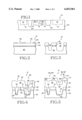
- FIG. 1 is a partial cross-section of an integrated circuit wafer after isolation trench fabrication and semiconductor device fabrication
- FIG. 2 is a partial cross-section of the wafer of FIG. 1 in the process of fabricating an isolation trench
- FIG. 3 is a partial cross-section of the wafer-in-process of FIG. 2 after etching isolation trench openings;
- FIG. 4 is a partial cross-section of the wafer-in-process of FIG. 3 after globally applying a layer of dielectric material to fill in the trench openings;
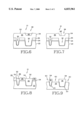
- FIG. 5 is a partial cross-section of the wafer-in-process of FIG. 4 after globally applying a protective layer over the dielectric layer;
- FIG. 6 is a partial cross-section of the wafer-in-process of FIG. 5 after a first global planarization process
- FIG. 7 is a partial cross-section of the wafer-in-process of FIG. 6 after stripping the protective layer;
- FIG. 8 is a partial cross-section of the wafer-in-process of FIG. 7 after performing a final global planarization process.
- FIG. 9 is a partial cross-section of the wafer-in-process of FIG. 8 after completing the trench isolation fabrication.
- FIG. 1 shows a cross-section of a portion of an integrated circuit wafer 10 including a plurality of devices 12, 14, 16.
- the device 14 includes a plurality of components 18.
- the term "active area" as used herein means an area 19 of the wafer 10 within which either a device or a device component is formed. Isolation trenches 20 are formed between the active areas so as to achieve higher device packing density and faster device speeds. Although, trenches of different depth may be formed as illustrated, in a preferred embodiment each trench 20 is to the same depth.
- FIGS. 2-9 show a portion of the wafer at various steps during an isolation trench fabrication process according to an embodiment of this invention. Typically the isolation trench fabrication process is performed prior to the device fabrication processes, or is intermixed with steps of the device fabrication process.
- a bare or partially doped silicon substrate 22 is cleaned and prepared for processing.
- a layer 24 of oxide material or another insulating material then is applied (e.g., grown) during a stress relief oxidation deposition process.
- Exemplary materials include silicon dioxide, and Si 3 N 4 .
- a layer 26 of protective material e.g., a nitride material
- a layer of photoresist 28 then is applied over the nitride layer 26. The photoresist layer is exposed using a desired mask to define areas of photoresist 28 with window areas 30 which reveal portions of the nitride layer 26.
- a trench etch step then is performed to form trench openings 32 in the window areas 30.
- the openings 32 are etched through the nitride layer 26, the oxide layer 24 and into the substrate 22.
- the photoresist 28 is stripped using either a wet or a dry stripping process.
- the oxide layer 24 is cleaned within the trench areas 32 and pulled back in part away from the corresponding edges of the nitride 28 and substrate 22 using an oxide precleaning process.
- an oxide layer 24' then is applied (e.g., grown) lining the trench opening 32 along the substrate 22. Either the same or a different insulating material is used for layer 24' as for layer 24.
- a trench fill process then is performed in which dielectric material 35, such as an oxide material, is deposited into the trench openings 32 and onto the nitride layer 26.
- dielectric material 35 such as an oxide material
- Exemplary dielectric materials include oxides, subatmospheric CVD, PECVD, or high density plasma oxide.
- a layer 34 of the dielectric material is shown in FIG. 4. The deposition process typically causes a uniform amount of material to be deposited. Because the contour surface to which the dielectric material 35 is deposited is not planar, the layer 34 does not have a planar contour. As shown in FIG. 4, there are recesses 36, 38 in the layer 34 overlaying the trench areas 32. The recesses 38 over wider trenches extend deeper than the recesses 36 over narrower trenches.
- the distal surface 39 of the layer 34 is cleaned and decontaminated.
- An annealing step then is performed during which the wafer-in-process 10 is heated in a furnace. The heating causes the dielectric material 35 to become denser adding to the non-planarity of the distal surface 39 of layer 34.
- the layer 34 has a thickness TH1 at a portion over the nitride layer 26 which is greater than the depth D1 of the trench opening 32 from a distal surface 41 of the nitride layer 26 to the base 42 of the trench area 32, (i.e., TH1>D1).
- the dielectric material 35 extends for a thickness D2 at the dielectric layer's 34 lowest contour 38' which is greater than thickness D1, (i.e., D2>D1).
- the thickness D2 extends from the base 42 of the trench 32 to the surface 38' within the deepest recess 38.
- the thickness D2 is greater than the thickness D1 by a distance which approximates the thickness D3 of the nitride layer 26, (i.e., D2-D1 ⁇ D3).
- thickness D2-D1 is greater than or equal to one-half the thickness D3, (i.e., D2-D1 ⁇ (0.5*D3).
- the thickness D2 is the same as the thickness TH1.
- a layer 44 of protective material 45 (e.g., a nitride material or other material as listed for the prior protective layer 26) is applied to the wafer-in-process 10 over the dielectric layer 34 after the annealing step. Such material may be the same or different than the material of layer 26.
- the distal surface 46 of protective layer 44 includes recesses 36", 38" overlaying the recesses 36, 38. The effect of the protective layer 44 is to decrease the area of the recesses 36, 38, and in particular to decrease the length/width or diameter of the recesses 36, 38. At the deepest portion of the deepest recess 38" in layer 44, the distal surface has part number 48.
- the thickness of the protective layer 44 is thickness D4.
- a first global planarizing process (e.g., mechanical planarization or chemical mechanical planarization) then is performed on the wafer-in-process 10.
- the planarizing reaches to at least the surfaces 39 and 48. In other embodiments the planarizing reaches past the surface 48. In other embodiments the planarizing reaches to within a few hundred angstroms of the surface 48.
- the planarizing step removes material 45 and 35 down to an approximate depth of the surface 48 of the deepest recess 38" as shown in FIG. 6.
- the effect of the layer 44 deposition and the global planarization is to eliminate the shallower recesses 36, 36", while protecting against dishing of the deeper recesses 38, 38".
- the protective material 45 is harder than the dielectric material 35. This allows the dielectric material 35 adjacent to the shallower recesses 36 to be removed countering any dishing of the protective material 45 in recess 36".
- the distal surface 50 of the wafer-in-process includes the dielectric material 35 in many portions and the protective material 45 in deep recess 38, 38" portions. Note that the contour of the distal surface 50 is more planar than the contour of the distal surface 39 after the trench filing step, but still not completely planar. Some dishing of the protective material 45 occurs within the recess 38 without dishing of the dielectric material 35 bordering the protective material 45.
- a wet stripping process is performed after the global planarization to remove the protective material 45 from the distal surface 50 of the wafer-in-process (i.e., from what is left of recess 38).
- a second global planarization process e.g., mechanical planarization or chemical mechanical planarization
- the second global planarization process removes the dielectric layer 34 over the portions of the nitride layer 26, and in some embodiments thins the nitride layer 26.
- the dielectric material 35 is softer than the nitride material 26.
- the distal surfaces 54 of the dielectric material 35 within the trenches 32 are generally planar and at no higher a level than the remaining nitride layer 26.
- the exposed surfaces 54, 26 then are cleaned and decontaminated.
- the remaining portions of the nitride layer 26 and the underlying portions of the oxide layer 24 are stripped. In some embodiments only the nitride layer 26 portions are stripped. In some embodiments the stripping is performed prior to the step of cleaning and decontaminating the distal surface 54 of the dielectric material 35 within the trench areas 32.
- FIG. 9 shows a portion of the wafer-in-process 10 upon completion of the trench isolation fabrication process. Thereafter, device fabrication processes are performed to achieve the integrated circuit wafer 10 of FIG. 1 having various devices 14, 16, 18, active areas 19 and isolation trenches 20.
- the isolation trenches 20 are the trenches of FIG. 9 as filled with the dielectric material 35. Doping and formation of gates, wiring lines, interconnects, contacts and vias occurs in the areas 60 in and over substrate 22 between the trenches 20 to define the active areas 19 (see FIG. 1) of devices 12, 14, 18 and device components 14.
Landscapes
- Engineering & Computer Science (AREA)
- Physics & Mathematics (AREA)
- Condensed Matter Physics & Semiconductors (AREA)
- General Physics & Mathematics (AREA)
- Manufacturing & Machinery (AREA)
- Computer Hardware Design (AREA)
- Microelectronics & Electronic Packaging (AREA)
- Power Engineering (AREA)
- Element Separation (AREA)
Abstract
Description
Claims (9)
Priority Applications (5)
| Application Number | Priority Date | Filing Date | Title |
|---|---|---|---|
| US09/071,051 US6033961A (en) | 1998-04-30 | 1998-04-30 | Isolation trench fabrication process |
| SG9804384A SG74095A1 (en) | 1998-04-30 | 1998-10-30 | Isolation trench fabrication process |
| JP11118718A JPH11330228A (en) | 1998-04-30 | 1999-04-26 | Method for forming isolating trench |
| EP99303359A EP0954023A1 (en) | 1998-04-30 | 1999-04-29 | Isolation trench fabrication process |
| KR1019990015356A KR100613939B1 (en) | 1998-04-30 | 1999-04-29 | Isolation trench fabrication process |
Applications Claiming Priority (1)
| Application Number | Priority Date | Filing Date | Title |
|---|---|---|---|
| US09/071,051 US6033961A (en) | 1998-04-30 | 1998-04-30 | Isolation trench fabrication process |
Publications (1)
| Publication Number | Publication Date |
|---|---|
| US6033961A true US6033961A (en) | 2000-03-07 |
Family
ID=22098939
Family Applications (1)
| Application Number | Title | Priority Date | Filing Date |
|---|---|---|---|
| US09/071,051 Expired - Fee Related US6033961A (en) | 1998-04-30 | 1998-04-30 | Isolation trench fabrication process |
Country Status (5)
| Country | Link |
|---|---|
| US (1) | US6033961A (en) |
| EP (1) | EP0954023A1 (en) |
| JP (1) | JPH11330228A (en) |
| KR (1) | KR100613939B1 (en) |
| SG (1) | SG74095A1 (en) |
Cited By (13)
| Publication number | Priority date | Publication date | Assignee | Title |
|---|---|---|---|---|
| US6235610B1 (en) * | 1998-01-13 | 2001-05-22 | Stmicroelectronics S.R.L. | Process for selectively implanting dopants into the bottom of a deep trench |
| US6284560B1 (en) * | 1998-12-18 | 2001-09-04 | Eastman Kodak Company | Method for producing co-planar surface structures |
| US6528389B1 (en) * | 1998-12-17 | 2003-03-04 | Lsi Logic Corporation | Substrate planarization with a chemical mechanical polishing stop layer |
| US20030211702A1 (en) * | 2002-05-07 | 2003-11-13 | Krishna Parat | Dual trench isolation using single critical lithographic patterning |
| US20040082181A1 (en) * | 1999-08-30 | 2004-04-29 | Doan Trung Tri | Methods of forming trench isolation regions |
| US20050009368A1 (en) * | 2003-07-07 | 2005-01-13 | Vaartstra Brian A. | Methods of forming a phosphorus doped silicon dioxide comprising layer, and methods of forming trench isolation in the fabrication of integrated circuitry |
| US20050054213A1 (en) * | 2003-09-05 | 2005-03-10 | Derderian Garo J. | Methods of depositing a silicon dioxide comprising layer in the fabrication of integrated circuitry, and methods of forming trench isolation in the fabrication of integrated circuitry |
| US20050208778A1 (en) * | 2004-03-22 | 2005-09-22 | Weimin Li | Methods of depositing silicon dioxide comprising layers in the fabrication of integrated circuitry, methods of forming trench isolation, and methods of forming arrays of memory cells |
| US20060046425A1 (en) * | 2004-08-31 | 2006-03-02 | Sandhu Gurtej S | Methods of forming trench isolation in the fabrication of integrated circuitry, methods of fabricating memory circuitry, integrated circuitry and memory integrated circuitry |
| US20060183294A1 (en) * | 2005-02-17 | 2006-08-17 | Micron Technology, Inc. | Methods of forming integrated circuitry |
| US20060197225A1 (en) * | 2005-03-07 | 2006-09-07 | Qi Pan | Electrically conductive line, method of forming an electrically conductive line, and method of reducing titanium silicide agglomeration in fabrication of titanium silicide over polysilicon transistor gate lines |
| US20060223279A1 (en) * | 2005-04-01 | 2006-10-05 | Micron Technology, Inc. | Methods of forming trench isolation in the fabrication of integrated circuitry and methods of fabricating integrated circuitry |
| US20110092061A1 (en) * | 2009-10-20 | 2011-04-21 | Yunjun Ho | Methods of Forming Silicon Oxides and Methods of Forming Interlevel Dielectrics |
Families Citing this family (1)
| Publication number | Priority date | Publication date | Assignee | Title |
|---|---|---|---|---|
| CN104103571B (en) * | 2013-04-15 | 2017-06-09 | 中芯国际集成电路制造(上海)有限公司 | The forming method of fleet plough groove isolation structure |
Citations (8)
| Publication number | Priority date | Publication date | Assignee | Title |
|---|---|---|---|---|
| US5229316A (en) * | 1992-04-16 | 1993-07-20 | Micron Technology, Inc. | Semiconductor processing method for forming substrate isolation trenches |
| US5712185A (en) * | 1996-04-23 | 1998-01-27 | United Microelectronics | Method for forming shallow trench isolation |
| US5923992A (en) * | 1997-02-11 | 1999-07-13 | Advanced Micro Devices, Inc. | Integrated circuit formed with shallow isolation structures having nitride placed on the trench dielectric |
| US5926713A (en) * | 1996-04-17 | 1999-07-20 | Advanced Micro Devices, Inc. | Method for achieving global planarization by forming minimum mesas in large field areas |
| US5930644A (en) * | 1997-07-23 | 1999-07-27 | Taiwan Semiconductor Manufacturing Co., Ltd. | Method of forming a shallow trench isolation using oxide slope etching |
| US5933748A (en) * | 1996-01-22 | 1999-08-03 | United Microelectronics Corp. | Shallow trench isolation process |
| US5940716A (en) * | 1996-03-15 | 1999-08-17 | Samsung Electronics Co., Ltd. | Methods of forming trench isolation regions using repatterned trench masks |
| US5945352A (en) * | 1997-12-19 | 1999-08-31 | Advanced Micro Devices | Method for fabrication of shallow isolation trenches with sloped wall profiles |
Family Cites Families (5)
| Publication number | Priority date | Publication date | Assignee | Title |
|---|---|---|---|---|
| US5665202A (en) * | 1995-11-24 | 1997-09-09 | Motorola, Inc. | Multi-step planarization process using polishing at two different pad pressures |
| JPH1022374A (en) * | 1996-07-08 | 1998-01-23 | Fujitsu Ltd | Manufacture of semiconductor device |
| US5721172A (en) * | 1996-12-02 | 1998-02-24 | Taiwan Semiconductor Manufacturing Company, Ltd. | Self-aligned polish stop layer hard masking method for forming planarized aperture fill layers |
| US5817567A (en) * | 1997-04-07 | 1998-10-06 | Taiwan Semiconductor Manufacturing Company Ltd. | Shallow trench isolation method |
| US5728621A (en) * | 1997-04-28 | 1998-03-17 | Chartered Semiconductor Manufacturing Pte Ltd | Method for shallow trench isolation |
-
1998
- 1998-04-30 US US09/071,051 patent/US6033961A/en not_active Expired - Fee Related
- 1998-10-30 SG SG9804384A patent/SG74095A1/en unknown
-
1999
- 1999-04-26 JP JP11118718A patent/JPH11330228A/en not_active Withdrawn
- 1999-04-29 KR KR1019990015356A patent/KR100613939B1/en not_active IP Right Cessation
- 1999-04-29 EP EP99303359A patent/EP0954023A1/en not_active Ceased
Patent Citations (8)
| Publication number | Priority date | Publication date | Assignee | Title |
|---|---|---|---|---|
| US5229316A (en) * | 1992-04-16 | 1993-07-20 | Micron Technology, Inc. | Semiconductor processing method for forming substrate isolation trenches |
| US5933748A (en) * | 1996-01-22 | 1999-08-03 | United Microelectronics Corp. | Shallow trench isolation process |
| US5940716A (en) * | 1996-03-15 | 1999-08-17 | Samsung Electronics Co., Ltd. | Methods of forming trench isolation regions using repatterned trench masks |
| US5926713A (en) * | 1996-04-17 | 1999-07-20 | Advanced Micro Devices, Inc. | Method for achieving global planarization by forming minimum mesas in large field areas |
| US5712185A (en) * | 1996-04-23 | 1998-01-27 | United Microelectronics | Method for forming shallow trench isolation |
| US5923992A (en) * | 1997-02-11 | 1999-07-13 | Advanced Micro Devices, Inc. | Integrated circuit formed with shallow isolation structures having nitride placed on the trench dielectric |
| US5930644A (en) * | 1997-07-23 | 1999-07-27 | Taiwan Semiconductor Manufacturing Co., Ltd. | Method of forming a shallow trench isolation using oxide slope etching |
| US5945352A (en) * | 1997-12-19 | 1999-08-31 | Advanced Micro Devices | Method for fabrication of shallow isolation trenches with sloped wall profiles |
Cited By (50)
| Publication number | Priority date | Publication date | Assignee | Title |
|---|---|---|---|---|
| US6235610B1 (en) * | 1998-01-13 | 2001-05-22 | Stmicroelectronics S.R.L. | Process for selectively implanting dopants into the bottom of a deep trench |
| US6528389B1 (en) * | 1998-12-17 | 2003-03-04 | Lsi Logic Corporation | Substrate planarization with a chemical mechanical polishing stop layer |
| US6284560B1 (en) * | 1998-12-18 | 2001-09-04 | Eastman Kodak Company | Method for producing co-planar surface structures |
| US6426237B2 (en) | 1998-12-18 | 2002-07-30 | Eastman Kodak Company | Method for producing optically planar surfaces for micro-electromechanical system devices |
| US20050239265A1 (en) * | 1999-08-30 | 2005-10-27 | Doan Trung T | Method of forming trench isolation regions |
| US20040082181A1 (en) * | 1999-08-30 | 2004-04-29 | Doan Trung Tri | Methods of forming trench isolation regions |
| US7012010B2 (en) | 1999-08-30 | 2006-03-14 | Micron Technology, Inc. | Methods of forming trench isolation regions |
| US20050239266A1 (en) * | 1999-08-30 | 2005-10-27 | Doan Trung T | Method of forming trench isolation regions |
| US20030211702A1 (en) * | 2002-05-07 | 2003-11-13 | Krishna Parat | Dual trench isolation using single critical lithographic patterning |
| US6849518B2 (en) * | 2002-05-07 | 2005-02-01 | Intel Corporation | Dual trench isolation using single critical lithographic patterning |
| US7790632B2 (en) | 2003-07-07 | 2010-09-07 | Micron Technology, Inc. | Methods of forming a phosphorus doped silicon dioxide-comprising layer |
| US20050009368A1 (en) * | 2003-07-07 | 2005-01-13 | Vaartstra Brian A. | Methods of forming a phosphorus doped silicon dioxide comprising layer, and methods of forming trench isolation in the fabrication of integrated circuitry |
| US20050124171A1 (en) * | 2003-07-07 | 2005-06-09 | Vaartstra Brian A. | Method of forming trench isolation in the fabrication of integrated circuitry |
| US7294556B2 (en) | 2003-07-07 | 2007-11-13 | Micron Technology, Inc. | Method of forming trench isolation in the fabrication of integrated circuitry |
| US20070161260A1 (en) * | 2003-07-07 | 2007-07-12 | Vaartstra Brian A | Methods of forming a phosphorus doped silicon dioxide-comprising layer |
| US7125815B2 (en) | 2003-07-07 | 2006-10-24 | Micron Technology, Inc. | Methods of forming a phosphorous doped silicon dioxide comprising layer |
| US20060183347A1 (en) * | 2003-09-05 | 2006-08-17 | Derderian Garo J | Method of depositing a silicon dioxide-comprising layer in the fabrication of integrated circuitry |
| US20050054213A1 (en) * | 2003-09-05 | 2005-03-10 | Derderian Garo J. | Methods of depositing a silicon dioxide comprising layer in the fabrication of integrated circuitry, and methods of forming trench isolation in the fabrication of integrated circuitry |
| US7250380B2 (en) | 2003-09-05 | 2007-07-31 | Micron Technology, Inc. | Method of depositing a silicon dioxide-comprising layer in the fabrication of integrated circuitry |
| US7250378B2 (en) | 2003-09-05 | 2007-07-31 | Micron Technology, Inc. | Method of depositing a silicon dioxide-comprising layer in the fabrication of integrated circuitry |
| US7429541B2 (en) | 2003-09-05 | 2008-09-30 | Micron Technology, Inc. | Method of forming trench isolation in the fabrication of integrated circuitry |
| US20060189158A1 (en) * | 2003-09-05 | 2006-08-24 | Derderian Garo J | Method of depositing a silicon dioxide-comprising layer in the fabrication of integrated circuitry |
| US20060189159A1 (en) * | 2003-09-05 | 2006-08-24 | Derderian Garo J | Methods of depositing a silicon dioxide comprising layer in the fabrication of integrated circuitry, and methods of forming trench isolation in the fabrication of integrated circuitry |
| US20060008972A1 (en) * | 2003-09-05 | 2006-01-12 | Derderian Garo J | Method of forming trench isolation in the fabrication of integrated circuitry |
| US7361614B2 (en) | 2003-09-05 | 2008-04-22 | Micron Technology, Inc. | Method of depositing a silicon dioxide comprising layer in the fabrication of integrated circuitry |
| US7157385B2 (en) | 2003-09-05 | 2007-01-02 | Micron Technology, Inc. | Method of depositing a silicon dioxide-comprising layer in the fabrication of integrated circuitry |
| US7470635B2 (en) | 2004-03-22 | 2008-12-30 | Micron Technology, Inc. | Method of depositing a silicon dioxide-comprising layer in the fabrication of integrated circuitry, methods of forming trench isolation in the fabrication of integrated circuitry, methods of depositing silicon dioxide-comprising layers in the fabrication of integrated circuitry, and methods of forming bit line over capacitor arrays of memory cells |
| US7053010B2 (en) | 2004-03-22 | 2006-05-30 | Micron Technology, Inc. | Methods of depositing silicon dioxide comprising layers in the fabrication of integrated circuitry, methods of forming trench isolation, and methods of forming arrays of memory cells |
| US20050208778A1 (en) * | 2004-03-22 | 2005-09-22 | Weimin Li | Methods of depositing silicon dioxide comprising layers in the fabrication of integrated circuitry, methods of forming trench isolation, and methods of forming arrays of memory cells |
| US20060160375A1 (en) * | 2004-03-22 | 2006-07-20 | Weimin Li | Method of depositing a silicon dioxide-comprising layer in the fabrication of integrated circuitry, methods of forming trench isolation in the fabrication of integrated circuitry, Method of depositing silicon dioxide-comprising layers in the fabrication of integrated circuitry, and methods of forming bit line over capacitor arrays of memory cells |
| US7364981B2 (en) | 2004-08-31 | 2008-04-29 | Micron Technology, Inc. | Methods of forming trench isolation in the fabrication of integrated circuitry, methods of fabricating memory circuitry, integrated circuitry and memory integrated circuitry |
| US20060046426A1 (en) * | 2004-08-31 | 2006-03-02 | Micron Technology, Inc. | Methods of forming trench isolation in the fabrication of integrated circuitry, methods of fabricating memory circuitry, integrated circuitry and memory integrated circuitry |
| US20070023856A1 (en) * | 2004-08-31 | 2007-02-01 | Sandhu Gurtej S | Methods of forming trench isolation in the fabrication of integrated circuitry, methods of fabricating memory circuitry, integrated circuitry and memory integrated circuitry |
| US20070020881A1 (en) * | 2004-08-31 | 2007-01-25 | Sandhu Gurtej S | Methods of forming trench isolation in the fabrication of integrated circuitry, methods of fabricating memory circuitry, integrated circuitry and memory integrated circuitry |
| US20060046425A1 (en) * | 2004-08-31 | 2006-03-02 | Sandhu Gurtej S | Methods of forming trench isolation in the fabrication of integrated circuitry, methods of fabricating memory circuitry, integrated circuitry and memory integrated circuitry |
| US7235459B2 (en) | 2004-08-31 | 2007-06-26 | Micron Technology, Inc. | Methods of forming trench isolation in the fabrication of integrated circuitry, methods of fabricating memory circuitry, integrated circuitry and memory integrated circuitry |
| US7368366B2 (en) | 2004-08-31 | 2008-05-06 | Micron Technology, Inc. | Methods of forming trench isolation in the fabrication of integrated circuitry, methods of fabricating memory circuitry, integrated circuitry and memory integrated circuitry |
| US7368800B2 (en) | 2004-08-31 | 2008-05-06 | Micron Technology, Inc. | Methods of forming trench isolation in the fabrication of integrated circuitry, methods of fabricating memory circuitry, integrated circuitry and memory integrated circuitry |
| US7387940B2 (en) | 2004-08-31 | 2008-06-17 | Micron Technology, Inc. | Methods of forming trench isolation in the fabrication of integrated circuitry, methods of fabricating memory circuitry, integrated circuitry and memory integrated circuitry |
| US7217634B2 (en) | 2005-02-17 | 2007-05-15 | Micron Technology, Inc. | Methods of forming integrated circuitry |
| US20060183294A1 (en) * | 2005-02-17 | 2006-08-17 | Micron Technology, Inc. | Methods of forming integrated circuitry |
| US7510966B2 (en) | 2005-03-07 | 2009-03-31 | Micron Technology, Inc. | Electrically conductive line, method of forming an electrically conductive line, and method of reducing titanium silicide agglomeration in fabrication of titanium silicide over polysilicon transistor gate lines |
| US20080284025A1 (en) * | 2005-03-07 | 2008-11-20 | Qi Pan | Electrically Conductive Line |
| US20060197225A1 (en) * | 2005-03-07 | 2006-09-07 | Qi Pan | Electrically conductive line, method of forming an electrically conductive line, and method of reducing titanium silicide agglomeration in fabrication of titanium silicide over polysilicon transistor gate lines |
| US20060223279A1 (en) * | 2005-04-01 | 2006-10-05 | Micron Technology, Inc. | Methods of forming trench isolation in the fabrication of integrated circuitry and methods of fabricating integrated circuitry |
| US8012847B2 (en) | 2005-04-01 | 2011-09-06 | Micron Technology, Inc. | Methods of forming trench isolation in the fabrication of integrated circuitry and methods of fabricating integrated circuitry |
| US8349699B2 (en) | 2005-04-01 | 2013-01-08 | Micron Technology, Inc. | Methods of forming trench isolation in the fabrication of integrated circuitry and methods of fabricating integrated circuitry |
| US20110092061A1 (en) * | 2009-10-20 | 2011-04-21 | Yunjun Ho | Methods of Forming Silicon Oxides and Methods of Forming Interlevel Dielectrics |
| US8105956B2 (en) | 2009-10-20 | 2012-01-31 | Micron Technology, Inc. | Methods of forming silicon oxides and methods of forming interlevel dielectrics |
| US8450218B2 (en) | 2009-10-20 | 2013-05-28 | Micron Technology, Inc. | Methods of forming silicon oxides and methods of forming interlevel dielectrics |
Also Published As
| Publication number | Publication date |
|---|---|
| EP0954023A1 (en) | 1999-11-03 |
| KR100613939B1 (en) | 2006-08-18 |
| JPH11330228A (en) | 1999-11-30 |
| SG74095A1 (en) | 2001-05-22 |
| KR19990083587A (en) | 1999-11-25 |
Similar Documents
| Publication | Publication Date | Title |
|---|---|---|
| US5492858A (en) | Shallow trench isolation process for high aspect ratio trenches | |
| US5270265A (en) | Stress relief technique of removing oxide from surface of trench-patterned semiconductor-on-insulator structure | |
| US5817568A (en) | Method of forming a trench isolation region | |
| US6033961A (en) | Isolation trench fabrication process | |
| US20020086497A1 (en) | Beaker shape trench with nitride pull-back for STI | |
| EP0813239A1 (en) | Improvements in or relating to semiconductor devices | |
| US20060118883A1 (en) | Trench in semiconductor device and formation method thereof | |
| US5928961A (en) | Dishing inhibited shallow trench isolation | |
| US6828213B2 (en) | Method to improve STI nano gap fill and moat nitride pull back | |
| US20070264790A1 (en) | Method of manufacturing semiconductor device | |
| US6380047B1 (en) | Shallow trench isolation formation with two source/drain masks and simplified planarization mask | |
| JPH08330410A (en) | Element isolating method, element isolating structure and semiconductor device | |
| KR100979230B1 (en) | The method for forming shall trench isolation in semiconductor device | |
| US7071072B2 (en) | Forming shallow trench isolation without the use of CMP | |
| JP3114062B2 (en) | Method for forming isolation film of semiconductor device | |
| KR20050028618A (en) | Method for forming isolation layer of semiconductor device | |
| KR20020050762A (en) | Method for isolating semiconductor devices | |
| GB2295487A (en) | Forming a field oxide layer to isolate semiconductor devices | |
| KR100672769B1 (en) | Method for forming isolation in semiconductor device | |
| JP3418386B2 (en) | Method for manufacturing semiconductor device | |
| KR100829375B1 (en) | Formation method of trench in semiconductor device | |
| KR100620701B1 (en) | Semiconductor Device Manufacturing Method for Compensating Divot of STI Oxide | |
| KR100422957B1 (en) | Method for forming isolation layer of semiconductor device | |
| KR20030059465A (en) | Method for forming trench isolation in semiconductor device | |
| KR20000033701A (en) | Method for manufacturing semiconductor device comprising flattening process when shallow trench isolation is formed |
Legal Events
| Date | Code | Title | Description |
|---|---|---|---|
| AS | Assignment |
Owner name: HEWLETT-PACKARD COMPANY, CALIFORNIA Free format text: ASSIGNMENT OF ASSIGNORS INTEREST;ASSIGNORS:XU, JIM-JUN;HADDAD, HOMAYOON;REEL/FRAME:009324/0051 Effective date: 19980430 |
|
| AS | Assignment |
Owner name: HEWLETT-PACKARD COMPANY, A DELAWARE CORPORATION, C Free format text: MERGER;ASSIGNOR:HEWLETT-PACKARD COMPANY, A CALIFORNIA CORPORATION;REEL/FRAME:010841/0649 Effective date: 19980520 |
|
| AS | Assignment |
Owner name: AGILENT TECHNOLOGIES INC, CALIFORNIA Free format text: ASSIGNMENT OF ASSIGNORS INTEREST;ASSIGNOR:HEWLETT-PACKARD COMPANY;REEL/FRAME:010977/0540 Effective date: 19991101 |
|
| AS | Assignment |
Owner name: AGILENT TECHNOLOGIES, CALIFORNIA Free format text: RE-RECORD TO CORRECT THE WRONG APPLICATION NO. AND FILING DATE REEL/FRAME 9324/0051;ASSIGNORS:XU, JIM-JUN;HADDAD, HOMAYOON;REEL/FRAME:010965/0008 Effective date: 19980430 |
|
| FEPP | Fee payment procedure |
Free format text: PAYOR NUMBER ASSIGNED (ORIGINAL EVENT CODE: ASPN); ENTITY STATUS OF PATENT OWNER: LARGE ENTITY |
|
| FPAY | Fee payment |
Year of fee payment: 4 |
|
| AS | Assignment |
Owner name: AVAGO TECHNOLOGIES GENERAL IP PTE. LTD., SINGAPORE Free format text: ASSIGNMENT OF ASSIGNORS INTEREST;ASSIGNOR:AGILENT TECHNOLOGIES, INC.;REEL/FRAME:017207/0020 Effective date: 20051201 |
|
| REMI | Maintenance fee reminder mailed | ||
| LAPS | Lapse for failure to pay maintenance fees | ||
| STCH | Information on status: patent discontinuation |
Free format text: PATENT EXPIRED DUE TO NONPAYMENT OF MAINTENANCE FEES UNDER 37 CFR 1.362 |
|
| FP | Lapsed due to failure to pay maintenance fee |
Effective date: 20080307 |
|
| AS | Assignment |
Owner name: AVAGO TECHNOLOGIES GENERAL IP (SINGAPORE) PTE. LTD Free format text: CORRECTIVE ASSIGNMENT TO CORRECT THE NAME OF THE ASSIGNEE PREVIOUSLY RECORDED ON REEL 017207 FRAME 0020. ASSIGNOR(S) HEREBY CONFIRMS THE ASSIGNMENT;ASSIGNOR:AGILENT TECHNOLOGIES, INC.;REEL/FRAME:038633/0001 Effective date: 20051201 |