US6033995A - Inverted layer epitaxial liftoff process - Google Patents
Inverted layer epitaxial liftoff process Download PDFInfo
- Publication number
- US6033995A US6033995A US08/931,695 US93169597A US6033995A US 6033995 A US6033995 A US 6033995A US 93169597 A US93169597 A US 93169597A US 6033995 A US6033995 A US 6033995A
- Authority
- US
- United States
- Prior art keywords
- adhesion promoter
- applying
- recited
- compound structure
- epilayers
- Prior art date
- Legal status (The legal status is an assumption and is not a legal conclusion. Google has not performed a legal analysis and makes no representation as to the accuracy of the status listed.)
- Expired - Lifetime
Links
- 238000000034 method Methods 0.000 title claims abstract description 52
- 230000008569 process Effects 0.000 title description 8
- 239000000758 substrate Substances 0.000 claims abstract description 110
- 239000004065 semiconductor Substances 0.000 claims abstract description 24
- GPXJNWSHGFTCBW-UHFFFAOYSA-N Indium phosphide Chemical compound [In]#P GPXJNWSHGFTCBW-UHFFFAOYSA-N 0.000 claims abstract description 6
- PMHQVHHXPFUNSP-UHFFFAOYSA-M copper(1+);methylsulfanylmethane;bromide Chemical compound Br[Cu].CSC PMHQVHHXPFUNSP-UHFFFAOYSA-M 0.000 claims abstract description 3
- 239000002318 adhesion promoter Substances 0.000 claims description 30
- 150000001875 compounds Chemical group 0.000 claims description 25
- 238000005530 etching Methods 0.000 claims description 8
- 238000000151 deposition Methods 0.000 claims description 7
- XLYOFNOQVPJJNP-UHFFFAOYSA-N water Substances O XLYOFNOQVPJJNP-UHFFFAOYSA-N 0.000 claims description 7
- BPSIOYPQMFLKFR-UHFFFAOYSA-N trimethoxy-[3-(oxiran-2-ylmethoxy)propyl]silane Chemical compound CO[Si](OC)(OC)CCCOCC1CO1 BPSIOYPQMFLKFR-UHFFFAOYSA-N 0.000 claims description 6
- WYTZZXDRDKSJID-UHFFFAOYSA-N (3-aminopropyl)triethoxysilane Chemical compound CCO[Si](OCC)(OCC)CCCN WYTZZXDRDKSJID-UHFFFAOYSA-N 0.000 claims description 5
- 238000003825 pressing Methods 0.000 claims description 5
- VEXZGXHMUGYJMC-UHFFFAOYSA-N Hydrochloric acid Chemical compound Cl VEXZGXHMUGYJMC-UHFFFAOYSA-N 0.000 claims description 4
- MHAJPDPJQMAIIY-UHFFFAOYSA-N Hydrogen peroxide Chemical compound OO MHAJPDPJQMAIIY-UHFFFAOYSA-N 0.000 claims description 4
- QAOWNCQODCNURD-UHFFFAOYSA-N Sulfuric acid Chemical compound OS(O)(=O)=O QAOWNCQODCNURD-UHFFFAOYSA-N 0.000 claims description 4
- 238000005304 joining Methods 0.000 claims description 4
- 239000000126 substance Substances 0.000 claims description 4
- 229910052738 indium Inorganic materials 0.000 claims 2
- APFVFJFRJDLVQX-UHFFFAOYSA-N indium atom Chemical compound [In] APFVFJFRJDLVQX-UHFFFAOYSA-N 0.000 claims 2
- GYHNNYVSQQEPJS-UHFFFAOYSA-N Gallium Chemical compound [Ga] GYHNNYVSQQEPJS-UHFFFAOYSA-N 0.000 claims 1
- 229910052733 gallium Inorganic materials 0.000 claims 1
- 239000000463 material Substances 0.000 abstract description 25
- 238000012545 processing Methods 0.000 abstract description 4
- 229910000530 Gallium indium arsenide Inorganic materials 0.000 abstract description 3
- KXNLCSXBJCPWGL-UHFFFAOYSA-N [Ga].[As].[In] Chemical compound [Ga].[As].[In] KXNLCSXBJCPWGL-UHFFFAOYSA-N 0.000 abstract description 3
- 239000002052 molecular layer Substances 0.000 abstract description 3
- JBRZTFJDHDCESZ-UHFFFAOYSA-N AsGa Chemical compound [As]#[Ga] JBRZTFJDHDCESZ-UHFFFAOYSA-N 0.000 description 10
- 229910001218 Gallium arsenide Inorganic materials 0.000 description 8
- 230000010354 integration Effects 0.000 description 5
- 239000000203 mixture Substances 0.000 description 5
- LFQSCWFLJHTTHZ-UHFFFAOYSA-N Ethanol Chemical compound CCO LFQSCWFLJHTTHZ-UHFFFAOYSA-N 0.000 description 4
- 230000003287 optical effect Effects 0.000 description 4
- 238000009987 spinning Methods 0.000 description 4
- XUIMIQQOPSSXEZ-UHFFFAOYSA-N Silicon Chemical compound [Si] XUIMIQQOPSSXEZ-UHFFFAOYSA-N 0.000 description 2
- XSTXAVWGXDQKEL-UHFFFAOYSA-N Trichloroethylene Chemical group ClC=C(Cl)Cl XSTXAVWGXDQKEL-UHFFFAOYSA-N 0.000 description 2
- 239000000853 adhesive Substances 0.000 description 2
- 230000001070 adhesive effect Effects 0.000 description 2
- MDPILPRLPQYEEN-UHFFFAOYSA-N aluminium arsenide Chemical compound [As]#[Al] MDPILPRLPQYEEN-UHFFFAOYSA-N 0.000 description 2
- 239000008367 deionised water Substances 0.000 description 2
- 230000008021 deposition Effects 0.000 description 2
- 229910003460 diamond Inorganic materials 0.000 description 2
- 239000010432 diamond Substances 0.000 description 2
- 238000007598 dipping method Methods 0.000 description 2
- 230000007613 environmental effect Effects 0.000 description 2
- 239000011521 glass Substances 0.000 description 2
- 229910052710 silicon Inorganic materials 0.000 description 2
- 239000010703 silicon Substances 0.000 description 2
- 238000012546 transfer Methods 0.000 description 2
- UBOXGVDOUJQMTN-UHFFFAOYSA-N trichloroethylene Natural products ClCC(Cl)Cl UBOXGVDOUJQMTN-UHFFFAOYSA-N 0.000 description 2
- PIGFYZPCRLYGLF-UHFFFAOYSA-N Aluminum nitride Chemical compound [Al]#N PIGFYZPCRLYGLF-UHFFFAOYSA-N 0.000 description 1
- 229910003556 H2 SO4 Inorganic materials 0.000 description 1
- 239000004642 Polyimide Substances 0.000 description 1
- 238000004026 adhesive bonding Methods 0.000 description 1
- 238000013459 approach Methods 0.000 description 1
- 230000009286 beneficial effect Effects 0.000 description 1
- 230000008878 coupling Effects 0.000 description 1
- 238000010168 coupling process Methods 0.000 description 1
- 238000005859 coupling reaction Methods 0.000 description 1
- 239000013078 crystal Substances 0.000 description 1
- 238000007496 glass forming Methods 0.000 description 1
- 230000006872 improvement Effects 0.000 description 1
- 238000004519 manufacturing process Methods 0.000 description 1
- 238000004377 microelectronic Methods 0.000 description 1
- 238000012986 modification Methods 0.000 description 1
- 230000004048 modification Effects 0.000 description 1
- 229920001721 polyimide Polymers 0.000 description 1
- 238000010897 surface acoustic wave method Methods 0.000 description 1
Images
Classifications
-
- H—ELECTRICITY
- H01—ELECTRIC ELEMENTS
- H01L—SEMICONDUCTOR DEVICES NOT COVERED BY CLASS H10
- H01L21/00—Processes or apparatus adapted for the manufacture or treatment of semiconductor or solid state devices or of parts thereof
- H01L21/70—Manufacture or treatment of devices consisting of a plurality of solid state components formed in or on a common substrate or of parts thereof; Manufacture of integrated circuit devices or of parts thereof
- H01L21/77—Manufacture or treatment of devices consisting of a plurality of solid state components or integrated circuits formed in, or on, a common substrate
- H01L21/78—Manufacture or treatment of devices consisting of a plurality of solid state components or integrated circuits formed in, or on, a common substrate with subsequent division of the substrate into plural individual devices
- H01L21/7806—Manufacture or treatment of devices consisting of a plurality of solid state components or integrated circuits formed in, or on, a common substrate with subsequent division of the substrate into plural individual devices involving the separation of the active layers from a substrate
-
- H—ELECTRICITY
- H01—ELECTRIC ELEMENTS
- H01L—SEMICONDUCTOR DEVICES NOT COVERED BY CLASS H10
- H01L2221/00—Processes or apparatus adapted for the manufacture or treatment of semiconductor or solid state devices or of parts thereof covered by H01L21/00
- H01L2221/67—Apparatus for handling semiconductor or electric solid state devices during manufacture or treatment thereof; Apparatus for handling wafers during manufacture or treatment of semiconductor or electric solid state devices or components; Apparatus not specifically provided for elsewhere
- H01L2221/683—Apparatus for handling semiconductor or electric solid state devices during manufacture or treatment thereof; Apparatus for handling wafers during manufacture or treatment of semiconductor or electric solid state devices or components; Apparatus not specifically provided for elsewhere for supporting or gripping
- H01L2221/68304—Apparatus for handling semiconductor or electric solid state devices during manufacture or treatment thereof; Apparatus for handling wafers during manufacture or treatment of semiconductor or electric solid state devices or components; Apparatus not specifically provided for elsewhere for supporting or gripping using temporarily an auxiliary support
- H01L2221/68368—Apparatus for handling semiconductor or electric solid state devices during manufacture or treatment thereof; Apparatus for handling wafers during manufacture or treatment of semiconductor or electric solid state devices or components; Apparatus not specifically provided for elsewhere for supporting or gripping using temporarily an auxiliary support used in a transfer process involving at least two transfer steps, i.e. including an intermediate handle substrate
Definitions
- the present invention relates to a method for integrating epitaxial semiconductor device layers with arbitrary host substrates, wherein the epilayers are grown on a growth substrate in an inverse order and joined to a host substrate in a manner that alleviates removal of the epilayers from the growth substrate prior to bonding the epilayers to the host substrate, and bonds the epilayers to the host substrate in a manner which maximizes the strength, yield, and the thermal conductivity of the resulting semiconductor device.
- ELO epitaxial liftoff process
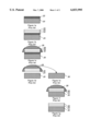
- a thin sacrificial (AlAs) or etch-stop layer 22 is grown on a growth substrate (GaAs) 20, as illustrated in FIG. 1a.
- Device epilayers are grown sequentially on the sacrificial layer beginning with a first device epilayer 24 and followed by a second device epilayer 26 until all epilayers are grown as required by the type of semiconductor device, shown in FIG. 1b.
- the device epilayers are covered with a wax-like material (Apiezon W) 28 prior to "liftoff", as shown in FIG. 1c.
- the GaAs epilayers are then "lifted off" from the growth substrate 20 by etching away the sacrificial layer 22, as illustrated in FIG. 1d.
- the GaAs epilayers are maintained suspended in the wax-like material 28 until they are bonded to the new host substrate 30, as shown in FIGS. 1e and 1f. Finally, the wax-like material 28 is removed, as shown in FIG. 1g.
- epitaxial liftoff provides, most significantly, a means to integrate high quality epilayers with "best match" host substrates
- the wax-like material used for the transfer of epilayers from growth to host substrates presents some problems.
- the wax-like material does not provide sufficient mechanical protection of the device epilayers, which in turn can cause electronic yield loss.
- the wax-like material needs to be dissolved in trichloroethylene and the use of trichloroethylene has associated environmental concerns.
- the use of the wax-like material also makes it impossible to align the "lifted off” epilayers to any pattern on the host substrate because of the opaque nature of the wax-like material.
- This method affords a strong bond with low optical loss but may not be optimal when bonding small device epilayers with substrates. Spinning a solution uniformly over a large and symmetric surface is easier than spinning the same solution on a small surface. In addition, dielectric bonds have very low thermal conductivity and are therefore not useful to make contact with thermally highly conductive host substrates.
- the "lift off” method disclosed above requires the use of a wax-like material to remove the device epilayers from the growth substrate and to transfer the device epilayers to the new host substrate.
- the use of such material poses a number of problems.
- additional processing steps are required for both the application and removal of the wax-like material.
- the solution required to dissolve the wax-like material poses environmental concerns.
- the fragile device epilayers, while suspended in the wax-like material are not provided with sufficient protection from mechanical damage, thus potentially jeopardizing the electronic yield of the semiconductor device.
- the wax-like material makes alignment of the device epilayers with patterns on host substrates difficult because of the opaqueness of the wax-like material.
- the present invention relates to methods for integrating device epilayers to host substrates by growing device epilayers in an inverse order on a growth substrate and effectively bonding device epilayers to host substrates.
- the inverse growth of the epitaxial layers allows the device epilayers to be joined to host substrates without the need for removing the device epilayers from the growth substrates prior to their being joined to host substrates. Consequently, the number and difficulty of steps required to integrate device epilayers with host substrates are reduced and the fragile device epilayers are better protected.
- a more effective bonding technique comprising mono-molecular layer forming, non-metallic adhesion promoters provides the following advantages: the epilayer to substrate bond is stronger, there is low thermal resistance between the device epilayer and host substrate, and the bonding layer is electrically insulating which is important for semiconductor devices used at mm-wave frequencies.
- the method comprises the steps of depositing a thin etch-stop layer on a growth substrate; growing the second device epilayer on the etch-stop layer; growing the first device epilayer on the second device epilayer; joining the device epilayers and the growth substrate to the host substrate by bonding the first device epilayer to a surface of the host substrate; and finally, selectively etching the growth substrate from the device epilayers.
- Another aspect of the present invention is to provide a method for bonding a device epilayer to a host substrate.
- the method comprising the steps of applying a layer of adhesion promoter between the device epilayer and the host substrate; joining the device epilayer to the host substrate to form a compound structure which contains the device epilayer and the host substrate; and finally, applying pressure to the compound structure while simultaneously baking the compound structure for a time and at a temperature sufficient to form chemical bonds between the adhesion promoter, the device epilayer, and the host substrate.
- FIGS. 1a-1g are illustrations of known epitaxial liftoff processing steps used for integrating device epilayers with arbitrary host substrates.
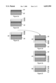
- FIGS. 2a-2f are illustrations of the steps used for integrating device epilayers with arbitrary substrates in accordance with the present invention.
- the present invention relates to an improvement in the method for integrating semiconductor device epilayers with arbitrary host substrates.
- One aspect of the invention is the inverse growth sequence of epitaxial device layers on growth substrates.
- the inverse growth sequence of device epilayers allows the device epilayers to be joined to host substrates without first separating the device epilayers from their growth substrate.
- the present invention relates to a method for bonding device epilayers with host substrates which allows the fabrication of semiconductor devices which are sturdy and have an optimal thermal contact between the device epilayer and host substrate.
- the principles of the present invention are applicable to many types of semiconductor devices, such as optical devices, surface acoustic wave devices, RF devices, and integrated sensors.
- the principles of the present invention are also applicable to many types of host substrates, such as silicon (Si), gallium arsenide (GaAs), and diamond.
- host substrates such as silicon (Si), gallium arsenide (GaAs), and diamond.
- Si silicon
- GaAs gallium arsenide
- the principles of the present invention are applicable to semiconductor devices which may require more than a first and second device epilayer.
- the number of device epilayers required for a semiconductor device depends on the type of semiconductor device. For illustration, the invention is described and illustrated further in FIGS. 2a through 2f with a growth substrate 32, etch-stop layer 34, second device epilayer 36, first device epilayer 38, and host substrate 42.
- the first step of the integration process is the deposition of an indium gallium arsenide (InGaAs) etch-stop layer 34 on a indium phosphide (InP) growth substrate 32.
- the growth substrate 32 composition is preferred for its compatibility with selective etching processes.
- the etch-stop layer 34 composition is preferred for its selective etching properties. It is important to note that other materials can be used for the growth substrate, host substrate, and etch-stop layer.
- the growth substrate may be gallium arsenide (GaAs).
- Host substrate choices may include silicon (Si) or diamond and etch-stop layers may include aluminum arsenide (AlAs).
- the host substrate 42 composition AlN
- AlN is preferred for its very close match of thermal expansion coefficients with indium phosphide (InP) epilayers and 200 W/mK thermal conductivity.
- material choices should be made according to the semiconductor application and thermal expansion match requirements.
- a second device epilayer 36 is grown on the etch-stop layer 34 and a first device epilayer 38 is grown on the second device epilayer 36. It is important to note from FIG. 2b that the device epilayers have been grown on the etch-stop layer 34 in an inverse order from the order in which they will be finally oriented on the host substrate 42. After the second device epilayer 36 and the first device epilayer 38 have been grown on the growth substrate 32, the device epilayers are joined to an aluminum nitride (AlN) host substrate 42, as illustrated in FIG. 2c.
- AlN aluminum nitride
- the bond between the first device epilayer 38 and the growth substrate 42 is formed by the application of mono-molecular layer forming adhesion promoters 46.
- ⁇ -amino-propyl-triethoxy-silane adhesion promoter solution is applied to the host substrate 42 by dipping the host substrate 42 in the ⁇ -amino-propyl-triethoxy-silane adhesion promoter solution.
- the ⁇ -amino-propyl-triethoxy-silane adhesion promoter solution is formed of approximately 93% ethanol, 5% water, and 2% ⁇ -amino-propyl-triethoxy-silane. Also, for the purposes of the illustrated embodiment, ⁇ -glycidyl-oxy-propyltrimethoxy-silane adhesion promoter solution is applied to the first device epilayer 38 by dipping the compound structure 40 in the ⁇ -glycidyl-oxy-propyl-trimethoxy-silane adhesion promoter solution.
- the ⁇ -glycidyl-oxy-propyl-trimethoxy-silane adhesion promoter solution is formed of approximately 93% ethanol, 5% water, and 2% ⁇ -glycidyl-oxypropyl-trimethoxy-silane.
- the preferred combined adhesion promoter thickness being from 1 to 10 nanometers.
- the first device epilayer 38 is joined to the host substrate 42, as shown in FIG. 2e, resulting in a compound structure 44.
- the compound structure 44 is then baked at a temperature of from 100° C. to 120° C. for a period of from 30 to 50 minutes while simultaneously applying a pressure of about 3 to 7 atmospheres.
- the preferred baking temperature is approximately 110°
- the preferred baking time is approximately 45 minutes while applying a pressure of approximately 5 atmospheres.
- the growth substrate 32 is separated from the second device epilayer 36 and first device epilayer 38.
- the growth substrate 32 is removed up to the etch-stop layer 34 in an aqueous hydrochloric acid solution and the etch-stop layer 34 is removed entirely in a sulfuric acid:hydrogen peroxide:water (H 2 SO 4 :H 2 O 2 :H 2 O) solution in a ratio of 1:1:50.
- a resulting semiconductor device 48 as illustrated in FIG. 2f, contains the second device epilayer 36 grown on the first device epilayer 38, and the first device epilayer 38 bonded to the host substrate 42.
- the semiconductor device 48 can now be further fabricated depending on the semiconductor device type.
Abstract
Description
Claims (17)
Priority Applications (1)
| Application Number | Priority Date | Filing Date | Title |
|---|---|---|---|
| US08/931,695 US6033995A (en) | 1997-09-16 | 1997-09-16 | Inverted layer epitaxial liftoff process |
Applications Claiming Priority (1)
| Application Number | Priority Date | Filing Date | Title |
|---|---|---|---|
| US08/931,695 US6033995A (en) | 1997-09-16 | 1997-09-16 | Inverted layer epitaxial liftoff process |
Publications (1)
| Publication Number | Publication Date |
|---|---|
| US6033995A true US6033995A (en) | 2000-03-07 |
Family
ID=25461195
Family Applications (1)
| Application Number | Title | Priority Date | Filing Date |
|---|---|---|---|
| US08/931,695 Expired - Lifetime US6033995A (en) | 1997-09-16 | 1997-09-16 | Inverted layer epitaxial liftoff process |
Country Status (1)
| Country | Link |
|---|---|
| US (1) | US6033995A (en) |
Cited By (62)
| Publication number | Priority date | Publication date | Assignee | Title |
|---|---|---|---|---|
| US6162702A (en) * | 1999-06-17 | 2000-12-19 | Intersil Corporation | Self-supported ultra thin silicon wafer process |
| US6214733B1 (en) * | 1999-11-17 | 2001-04-10 | Elo Technologies, Inc. | Process for lift off and handling of thin film materials |
| US20020084000A1 (en) * | 1997-06-24 | 2002-07-04 | Eugene A. Fitzgerald | Controlling threading dislocation densities in Ge on Si using graded GeSi layers and planarization |
| KR100366706B1 (en) * | 2000-04-27 | 2003-01-09 | 삼성코닝 주식회사 | Method for fabricating a GaN single crystal substrate |
| US20030077867A1 (en) * | 2001-03-02 | 2003-04-24 | Fitzergald Eugene A. | Relaxed silicon germanium platform for high speed CMOS electronics and high speed analog circuits |
| US6562648B1 (en) * | 2000-08-23 | 2003-05-13 | Xerox Corporation | Structure and method for separation and transfer of semiconductor thin films onto dissimilar substrate materials |
| US6573126B2 (en) | 2000-08-16 | 2003-06-03 | Massachusetts Institute Of Technology | Process for producing semiconductor article using graded epitaxial growth |
| US20030102498A1 (en) * | 2001-09-24 | 2003-06-05 | Glyn Braithwaite | RF circuits including transistors having strained material layers |
| US20030113948A1 (en) * | 2000-01-20 | 2003-06-19 | Amberwave Systems Corporation | Low threading dislocation density relaxed mismatched epilayers without high temperature growth |
| US6602613B1 (en) | 2000-01-20 | 2003-08-05 | Amberwave Systems Corporation | Heterointegration of materials using deposition and bonding |
| US20030170965A1 (en) * | 2001-12-27 | 2003-09-11 | Seiko Epson Corporation | Semiconductor integrated circuit and method for manufacturing semiconductor integrated circuit |
| US20030170946A1 (en) * | 2001-12-28 | 2003-09-11 | Seiko Epson Corporation | Semiconductor integrated circuit and method for manufacturing semiconductor integrated circuit |
| US6649480B2 (en) | 2000-12-04 | 2003-11-18 | Amberwave Systems Corporation | Method of fabricating CMOS inverter and integrated circuits utilizing strained silicon surface channel MOSFETs |
| US20030227029A1 (en) * | 2002-06-07 | 2003-12-11 | Amberwave Systems Corporation | Elevated source and drain elements for strained-channel heterojuntion field-effect transistors |
| US20030227057A1 (en) * | 2002-06-07 | 2003-12-11 | Lochtefeld Anthony J. | Strained-semiconductor-on-insulator device structures |
| US20040000268A1 (en) * | 1998-04-10 | 2004-01-01 | Massachusetts Institute Of Technology | Etch stop layer system |
| US20040005740A1 (en) * | 2002-06-07 | 2004-01-08 | Amberwave Systems Corporation | Strained-semiconductor-on-insulator device structures |
| US20040007709A1 (en) * | 2002-06-10 | 2004-01-15 | Seiko Epson Corporation | Semiconductor integrated circuit, signal transmitting device, electro-optical device, and electronic apparatus |
| US20040016932A1 (en) * | 2002-05-30 | 2004-01-29 | Seiko Epson Corporation | Semiconductor unit, semiconductor apparatus, and method for making the same, electrooptic apparatus, and electronic apparatus |
| US20040031979A1 (en) * | 2002-06-07 | 2004-02-19 | Amberwave Systems Corporation | Strained-semiconductor-on-insulator device structures |
| US20040036074A1 (en) * | 2002-06-18 | 2004-02-26 | Seiko Epson Corporation | Optical interconnection integrated circuit, method of manufacturing optical interconnection integrated circuit, electro-optical apparatus, and electronic apparatus |
| US20040036078A1 (en) * | 2002-06-20 | 2004-02-26 | Seiko Epson Corporation | Semiconductor device, method of manufacturing the same, electro-optic device and electronic apparatus |
| US20040040493A1 (en) * | 2002-08-30 | 2004-03-04 | Amberwave Systems Corporation | Reduction of dislocation pile-up formation during relaxed lattice-mismatched epitaxy |
| US6703688B1 (en) | 2001-03-02 | 2004-03-09 | Amberwave Systems Corporation | Relaxed silicon germanium platform for high speed CMOS electronics and high speed analog circuits |
| US20040048447A1 (en) * | 2002-07-11 | 2004-03-11 | Seiko Epson Corporation | Method for making semiconductor device, semiconductor element composite, electro-optical apparatus, and electronic system |
| US6724008B2 (en) | 2001-03-02 | 2004-04-20 | Amberwave Systems Corporation | Relaxed silicon germanium platform for high speed CMOS electronics and high speed analog circuits |
| US20040075105A1 (en) * | 2002-08-23 | 2004-04-22 | Amberwave Systems Corporation | Semiconductor heterostructures having reduced dislocation pile-ups and related methods |
| US20040075149A1 (en) * | 2000-12-04 | 2004-04-22 | Amberwave Systems Corporation | CMOS inverter and integrated circuits utilizing strained silicon surface channel MOSFETs |
| US20040109629A1 (en) * | 2002-10-01 | 2004-06-10 | Seiko Epson Corporation | Optical interconnection circuit, manufacturing method thereof, electro-optical device and electronic equipment |
| US6750130B1 (en) * | 2000-01-20 | 2004-06-15 | Amberwave Systems Corporation | Heterointegration of materials using deposition and bonding |
| US20040136639A1 (en) * | 2002-11-20 | 2004-07-15 | Seiko Epson Corporation | Optical interconnection circuit between chips, electrooptical device and electronic equipment |
| US6780703B2 (en) | 2002-08-27 | 2004-08-24 | Freescale Semiconductor, Inc. | Method for forming a semiconductor device |
| US20040219726A1 (en) * | 2001-03-02 | 2004-11-04 | Amberwave Systems Corporation | Methods of fabricating contact regions for FET incorporating SiGe |
| US20040218874A1 (en) * | 2003-02-28 | 2004-11-04 | Seiko Epson Corporation | Fiber optic transceiver module, manufacturing method thereof, and electronic equipment |
| US20050042849A1 (en) * | 2002-06-25 | 2005-02-24 | Amberwave Systems Corporation | Reacted conductive gate electrodes |
| US20050054168A1 (en) * | 2001-09-21 | 2005-03-10 | Amberwave Systems Corporation | Semiconductor structures employing strained material layers with defined impurity gradients and methods for fabricating same |
| US20050104083A1 (en) * | 2000-08-31 | 2005-05-19 | Osram Opto Semiconductors Gmbh | Method for fabricating a radiation-emitting semiconductor chip based on Ill-V nitride semiconductor |
| US20050136624A1 (en) * | 2001-04-04 | 2005-06-23 | Massachusetts Institute Of Technology | Method for semiconductor device fabrication |
| US20050176204A1 (en) * | 2002-06-10 | 2005-08-11 | Amberwave Systems Corporation | Source and drain elements |
| US20050205859A1 (en) * | 2003-03-07 | 2005-09-22 | Amberwave Systems Corporation | Shallow trench isolation process |
| US20050227455A1 (en) * | 2004-03-29 | 2005-10-13 | Jongkook Park | Method of separating layers of material |
| KR100525307B1 (en) * | 2002-03-29 | 2005-11-02 | (주)나울 | Thermal protection glassing using nanopartics |
| US20050247950A1 (en) * | 2004-05-06 | 2005-11-10 | Cree, Inc. | Lift-off process for GaN films formed on SiC substrates and devices fabricated using the method |
| US20060011984A1 (en) * | 2002-06-07 | 2006-01-19 | Amberwave Systems Corporation | Control of strain in device layers by selective relaxation |
| US20060014366A1 (en) * | 2002-06-07 | 2006-01-19 | Amberwave Systems Corporation | Control of strain in device layers by prevention of relaxation |
| US20060091103A1 (en) * | 2004-10-29 | 2006-05-04 | Hitachi Global Storage Technologies Netherlands, B.V | Write head fabrication by inverting order of process steps |
| US20060113605A1 (en) * | 2004-12-01 | 2006-06-01 | Amberwave Systems Corporation | Hybrid fin field-effect transistor structures and related methods |
| US20060113603A1 (en) * | 2004-12-01 | 2006-06-01 | Amberwave Systems Corporation | Hybrid semiconductor-on-insulator structures and related methods |
| US7060632B2 (en) | 2002-03-14 | 2006-06-13 | Amberwave Systems Corporation | Methods for fabricating strained layers on semiconductor substrates |
| US7096640B1 (en) * | 2003-05-30 | 2006-08-29 | Traco | Thermal breaking system for construction materials and the like |
| US20070147761A1 (en) * | 2005-10-07 | 2007-06-28 | Kwakernaak Martin H | Amorphous silicon waveguides on lll/V substrates with barrier layer |
| US7244308B2 (en) * | 1999-12-03 | 2007-07-17 | Sony Corporation | Method of manufacturing crystal of III-V compound of the nitride system, crystal substrate of III-V compound of the nitride system, crystal film of III-V compound of the nitride system, and method of manufacturing device |
| US20070181246A1 (en) * | 2003-11-28 | 2007-08-09 | Semiconductor Energy Laboratory Co., Ltd. | Method of manufacturing display device |
| US20070249104A1 (en) * | 2006-04-24 | 2007-10-25 | Han-Tu Lin | Method for fabricating a thin-film transistor |
| US7332417B2 (en) | 2003-01-27 | 2008-02-19 | Amberwave Systems Corporation | Semiconductor structures with structural homogeneity |
| US20080067499A1 (en) * | 2006-09-15 | 2008-03-20 | Sharp Laboratories Of America, Inc. | Silicon/germanium superlattice thermal sensor |
| US20080282628A1 (en) * | 2007-05-16 | 2008-11-20 | Three Rivers Aluminum Company D/B/A Traco | Construction product having a moveable element with multi-functional thermal break |
| US20080282627A1 (en) * | 2007-05-16 | 2008-11-20 | Three Rivers Aluminum Company D/B/A Traco | Construction product having a frame with multi-functional thermal break |
| US20100254425A1 (en) * | 2007-06-29 | 2010-10-07 | International Business Machines Corporation | Phase change material based temperature sensor |
| US8981641B2 (en) | 2003-10-28 | 2015-03-17 | Semiconductor Energy Laboratory Co., Ltd. | Method of manufacturing optical film |
| CN110970340A (en) * | 2019-10-31 | 2020-04-07 | 中国电子科技集团公司第五十五研究所 | Flexible InP HBT device and preparation method thereof |
| US10658998B2 (en) | 2013-07-31 | 2020-05-19 | Oepic Semiconductors, Inc. | Piezoelectric film transfer for acoustic resonators and filters |
Citations (8)
| Publication number | Priority date | Publication date | Assignee | Title |
|---|---|---|---|---|
| US3773707A (en) * | 1969-02-20 | 1973-11-20 | Bayer Ag | Polyamide molding composition containing plagioclase feldspar |
| US4509063A (en) * | 1982-07-26 | 1985-04-02 | Canon Kabushiki Kaisha | Ink jet recording head with delaminating feature |
| US4732858A (en) * | 1986-09-17 | 1988-03-22 | Brewer Science, Inc. | Adhesion promoting product and process for treating an integrated circuit substrate |
| US4952535A (en) * | 1989-07-19 | 1990-08-28 | Corning Incorporated | Aluminum nitride bodies and method |
| US5286335A (en) * | 1992-04-08 | 1994-02-15 | Georgia Tech Research Corporation | Processes for lift-off and deposition of thin film materials |
| US5376579A (en) * | 1993-07-02 | 1994-12-27 | The United States Of America As Represented By The Secretary Of The Air Force | Schemes to form silicon-on-diamond structure |
| US5462883A (en) * | 1991-06-28 | 1995-10-31 | International Business Machines Corporation | Method of fabricating defect-free silicon on an insulating substrate |
| US5527872A (en) * | 1990-09-14 | 1996-06-18 | At&T Global Information Solutions Company | Electronic device with a spin-on glass dielectric layer |
-
1997
- 1997-09-16 US US08/931,695 patent/US6033995A/en not_active Expired - Lifetime
Patent Citations (8)
| Publication number | Priority date | Publication date | Assignee | Title |
|---|---|---|---|---|
| US3773707A (en) * | 1969-02-20 | 1973-11-20 | Bayer Ag | Polyamide molding composition containing plagioclase feldspar |
| US4509063A (en) * | 1982-07-26 | 1985-04-02 | Canon Kabushiki Kaisha | Ink jet recording head with delaminating feature |
| US4732858A (en) * | 1986-09-17 | 1988-03-22 | Brewer Science, Inc. | Adhesion promoting product and process for treating an integrated circuit substrate |
| US4952535A (en) * | 1989-07-19 | 1990-08-28 | Corning Incorporated | Aluminum nitride bodies and method |
| US5527872A (en) * | 1990-09-14 | 1996-06-18 | At&T Global Information Solutions Company | Electronic device with a spin-on glass dielectric layer |
| US5462883A (en) * | 1991-06-28 | 1995-10-31 | International Business Machines Corporation | Method of fabricating defect-free silicon on an insulating substrate |
| US5286335A (en) * | 1992-04-08 | 1994-02-15 | Georgia Tech Research Corporation | Processes for lift-off and deposition of thin film materials |
| US5376579A (en) * | 1993-07-02 | 1994-12-27 | The United States Of America As Represented By The Secretary Of The Air Force | Schemes to form silicon-on-diamond structure |
Cited By (157)
| Publication number | Priority date | Publication date | Assignee | Title |
|---|---|---|---|---|
| US7081410B2 (en) | 1997-06-24 | 2006-07-25 | Massachusetts Institute Of Technology | Controlling threading dislocation densities in Ge on Si using graded GeSi layers and planarization |
| US20020084000A1 (en) * | 1997-06-24 | 2002-07-04 | Eugene A. Fitzgerald | Controlling threading dislocation densities in Ge on Si using graded GeSi layers and planarization |
| US20040262631A1 (en) * | 1997-06-24 | 2004-12-30 | Massachusetts Institute Of Technology | Controlling threading dislocation densities in Ge on Si using graded GeSi layers and planarization |
| US7250359B2 (en) | 1997-06-24 | 2007-07-31 | Massachusetts Institute Of Technology | Controlling threading dislocation densities in Ge on Si using graded GeSi layers and planarization |
| US6876010B1 (en) | 1997-06-24 | 2005-04-05 | Massachusetts Institute Of Technology | Controlling threading dislocation densities in Ge on Si using graded GeSi layers and planarization |
| US20040000268A1 (en) * | 1998-04-10 | 2004-01-01 | Massachusetts Institute Of Technology | Etch stop layer system |
| US7227176B2 (en) | 1998-04-10 | 2007-06-05 | Massachusetts Institute Of Technology | Etch stop layer system |
| US6162702A (en) * | 1999-06-17 | 2000-12-19 | Intersil Corporation | Self-supported ultra thin silicon wafer process |
| US6214733B1 (en) * | 1999-11-17 | 2001-04-10 | Elo Technologies, Inc. | Process for lift off and handling of thin film materials |
| US7244308B2 (en) * | 1999-12-03 | 2007-07-17 | Sony Corporation | Method of manufacturing crystal of III-V compound of the nitride system, crystal substrate of III-V compound of the nitride system, crystal film of III-V compound of the nitride system, and method of manufacturing device |
| US6703144B2 (en) | 2000-01-20 | 2004-03-09 | Amberwave Systems Corporation | Heterointegration of materials using deposition and bonding |
| US6750130B1 (en) * | 2000-01-20 | 2004-06-15 | Amberwave Systems Corporation | Heterointegration of materials using deposition and bonding |
| US6602613B1 (en) | 2000-01-20 | 2003-08-05 | Amberwave Systems Corporation | Heterointegration of materials using deposition and bonding |
| US20030113948A1 (en) * | 2000-01-20 | 2003-06-19 | Amberwave Systems Corporation | Low threading dislocation density relaxed mismatched epilayers without high temperature growth |
| US6864115B2 (en) | 2000-01-20 | 2005-03-08 | Amberwave Systems Corporation | Low threading dislocation density relaxed mismatched epilayers without high temperature growth |
| KR100366706B1 (en) * | 2000-04-27 | 2003-01-09 | 삼성코닝 주식회사 | Method for fabricating a GaN single crystal substrate |
| US6573126B2 (en) | 2000-08-16 | 2003-06-03 | Massachusetts Institute Of Technology | Process for producing semiconductor article using graded epitaxial growth |
| US20050009288A1 (en) * | 2000-08-16 | 2005-01-13 | Massachusetts Institute Of Technology | Process for producing semiconductor article using graded epitaxial growth |
| US20040173791A1 (en) * | 2000-08-16 | 2004-09-09 | Massachusetts Institute Of Technology | Semiconductor substrate structure |
| US20030168654A1 (en) * | 2000-08-16 | 2003-09-11 | Massachusetts Institute Of Technology | Process for producing semiconductor article using graded epitaxial growth |
| US6713326B2 (en) | 2000-08-16 | 2004-03-30 | Masachusetts Institute Of Technology | Process for producing semiconductor article using graded epitaxial growth |
| US6737670B2 (en) | 2000-08-16 | 2004-05-18 | Massachusetts Institute Of Technology | Semiconductor substrate structure |
| US6921914B2 (en) | 2000-08-16 | 2005-07-26 | Massachusetts Institute Of Technology | Process for producing semiconductor article using graded epitaxial growth |
| US6562648B1 (en) * | 2000-08-23 | 2003-05-13 | Xerox Corporation | Structure and method for separation and transfer of semiconductor thin films onto dissimilar substrate materials |
| US7105370B2 (en) * | 2000-08-31 | 2006-09-12 | Osram Gmbh | Method for fabricating a radiation-emitting semiconductor chip based on III-V nitride semiconductor |
| US20050104083A1 (en) * | 2000-08-31 | 2005-05-19 | Osram Opto Semiconductors Gmbh | Method for fabricating a radiation-emitting semiconductor chip based on Ill-V nitride semiconductor |
| US20040075149A1 (en) * | 2000-12-04 | 2004-04-22 | Amberwave Systems Corporation | CMOS inverter and integrated circuits utilizing strained silicon surface channel MOSFETs |
| US6881632B2 (en) | 2000-12-04 | 2005-04-19 | Amberwave Systems Corporation | Method of fabricating CMOS inverter and integrated circuits utilizing strained surface channel MOSFETS |
| US20050106850A1 (en) * | 2000-12-04 | 2005-05-19 | Amberwave Systems Corporation | Method of fabricating CMOS inverter and integrated circuits utilizing strained surface channel MOSFETs |
| US6649480B2 (en) | 2000-12-04 | 2003-11-18 | Amberwave Systems Corporation | Method of fabricating CMOS inverter and integrated circuits utilizing strained silicon surface channel MOSFETs |
| US20060275972A1 (en) * | 2000-12-04 | 2006-12-07 | Amberwave Systems Corporation | Method of fabricating CMOS inverters and integrated circuits utilizing strained surface channel MOSFETs |
| US20040219726A1 (en) * | 2001-03-02 | 2004-11-04 | Amberwave Systems Corporation | Methods of fabricating contact regions for FET incorporating SiGe |
| US6724008B2 (en) | 2001-03-02 | 2004-04-20 | Amberwave Systems Corporation | Relaxed silicon germanium platform for high speed CMOS electronics and high speed analog circuits |
| US6723661B2 (en) | 2001-03-02 | 2004-04-20 | Amberwave Systems Corporation | Relaxed silicon germanium platform for high speed CMOS electronics and high speed analog circuits |
| US6703688B1 (en) | 2001-03-02 | 2004-03-09 | Amberwave Systems Corporation | Relaxed silicon germanium platform for high speed CMOS electronics and high speed analog circuits |
| US20050077511A1 (en) * | 2001-03-02 | 2005-04-14 | Amberwave Systems Corporation | Relaxed SiGe platform for high speed CMOS electronics and high speed analog circuits |
| US8822282B2 (en) | 2001-03-02 | 2014-09-02 | Taiwan Semiconductor Manufacturing Company, Ltd. | Methods of fabricating contact regions for FET incorporating SiGe |
| US20040161947A1 (en) * | 2001-03-02 | 2004-08-19 | Amberware Systems Corporation | Relaxed SiGe platform for high speed CMOS electronics and high speed analog circuits |
| US20030077867A1 (en) * | 2001-03-02 | 2003-04-24 | Fitzergald Eugene A. | Relaxed silicon germanium platform for high speed CMOS electronics and high speed analog circuits |
| US7348259B2 (en) | 2001-04-04 | 2008-03-25 | Massachusetts Institute Of Technology | Method of fabricating a semiconductor structure that includes transferring one or more material layers to a substrate and smoothing an exposed surface of at least one of the material layers |
| US20050136624A1 (en) * | 2001-04-04 | 2005-06-23 | Massachusetts Institute Of Technology | Method for semiconductor device fabrication |
| US6940089B2 (en) | 2001-04-04 | 2005-09-06 | Massachusetts Institute Of Technology | Semiconductor device structure |
| US7846802B2 (en) | 2001-09-21 | 2010-12-07 | Taiwan Semiconductor Manufacturing Company, Ltd. | Semiconductor structures employing strained material layers with defined impurity gradients and methods for fabricating same |
| US7884353B2 (en) | 2001-09-21 | 2011-02-08 | Taiwan Semiconductor Manufacturing Company, Ltd. | Semiconductor structures employing strained material layers with defined impurity gradients and methods for fabricating same |
| US7776697B2 (en) | 2001-09-21 | 2010-08-17 | Taiwan Semiconductor Manufacturing Company, Ltd. | Semiconductor structures employing strained material layers with defined impurity gradients and methods for fabricating same |
| US20050054168A1 (en) * | 2001-09-21 | 2005-03-10 | Amberwave Systems Corporation | Semiconductor structures employing strained material layers with defined impurity gradients and methods for fabricating same |
| US20070293003A1 (en) * | 2001-09-21 | 2007-12-20 | Matthew Currie | Semiconductor structures employing strained material layers with defined impurity gradients and methods for fabricating same |
| US20030102498A1 (en) * | 2001-09-24 | 2003-06-05 | Glyn Braithwaite | RF circuits including transistors having strained material layers |
| US7906776B2 (en) | 2001-09-24 | 2011-03-15 | Taiwan Semiconductor Manufacturing Company, Ltd. | RF circuits including transistors having strained material layers |
| US6933518B2 (en) | 2001-09-24 | 2005-08-23 | Amberwave Systems Corporation | RF circuits including transistors having strained material layers |
| US7709828B2 (en) | 2001-09-24 | 2010-05-04 | Taiwan Semiconductor Manufacturing Company, Ltd. | RF circuits including transistors having strained material layers |
| US7244662B2 (en) | 2001-12-27 | 2007-07-17 | Seiko Epson Corporation | Method for manufacturing semiconductor integrated circuit |
| US20030170965A1 (en) * | 2001-12-27 | 2003-09-11 | Seiko Epson Corporation | Semiconductor integrated circuit and method for manufacturing semiconductor integrated circuit |
| US20030170946A1 (en) * | 2001-12-28 | 2003-09-11 | Seiko Epson Corporation | Semiconductor integrated circuit and method for manufacturing semiconductor integrated circuit |
| US6858518B2 (en) | 2001-12-28 | 2005-02-22 | Seiko Epson Corporation | Method for manufacturing semiconductor integrated circuit |
| US7060632B2 (en) | 2002-03-14 | 2006-06-13 | Amberwave Systems Corporation | Methods for fabricating strained layers on semiconductor substrates |
| US7259108B2 (en) | 2002-03-14 | 2007-08-21 | Amberwave Systems Corporation | Methods for fabricating strained layers on semiconductor substrates |
| KR100525307B1 (en) * | 2002-03-29 | 2005-11-02 | (주)나울 | Thermal protection glassing using nanopartics |
| US7180924B2 (en) | 2002-05-30 | 2007-02-20 | Seiko Epson Corporation | Semiconductor apparatus and a semiconductor unit, the semiconductor unit including a functional layer including a semiconductor element, and a highly conductive layer |
| US20040016932A1 (en) * | 2002-05-30 | 2004-01-29 | Seiko Epson Corporation | Semiconductor unit, semiconductor apparatus, and method for making the same, electrooptic apparatus, and electronic apparatus |
| US7074623B2 (en) | 2002-06-07 | 2006-07-11 | Amberwave Systems Corporation | Methods of forming strained-semiconductor-on-insulator finFET device structures |
| US20040031979A1 (en) * | 2002-06-07 | 2004-02-19 | Amberwave Systems Corporation | Strained-semiconductor-on-insulator device structures |
| US20030227029A1 (en) * | 2002-06-07 | 2003-12-11 | Amberwave Systems Corporation | Elevated source and drain elements for strained-channel heterojuntion field-effect transistors |
| US20050205934A1 (en) * | 2002-06-07 | 2005-09-22 | Amberwave Systems Corporation | Strained germanium-on-insulator device structures |
| US20050212061A1 (en) * | 2002-06-07 | 2005-09-29 | Amberwave Systems Corporation | Methods for forming strained-semiconductor-on-insulator device structures by use of cleave planes |
| US8748292B2 (en) | 2002-06-07 | 2014-06-10 | Taiwan Semiconductor Manufacturing Company, Ltd. | Methods of forming strained-semiconductor-on-insulator device structures |
| US20080128751A1 (en) * | 2002-06-07 | 2008-06-05 | Amberwave Systems Corporation | Methods for forming iii-v semiconductor device structures |
| US7335545B2 (en) | 2002-06-07 | 2008-02-26 | Amberwave Systems Corporation | Control of strain in device layers by prevention of relaxation |
| US20050280103A1 (en) * | 2002-06-07 | 2005-12-22 | Amberwave Systems Corporation | Strained-semiconductor-on-insulator finFET device structures |
| US20030227057A1 (en) * | 2002-06-07 | 2003-12-11 | Lochtefeld Anthony J. | Strained-semiconductor-on-insulator device structures |
| US20060011984A1 (en) * | 2002-06-07 | 2006-01-19 | Amberwave Systems Corporation | Control of strain in device layers by selective relaxation |
| US20060014366A1 (en) * | 2002-06-07 | 2006-01-19 | Amberwave Systems Corporation | Control of strain in device layers by prevention of relaxation |
| US6995430B2 (en) | 2002-06-07 | 2006-02-07 | Amberwave Systems Corporation | Strained-semiconductor-on-insulator device structures |
| US20040005740A1 (en) * | 2002-06-07 | 2004-01-08 | Amberwave Systems Corporation | Strained-semiconductor-on-insulator device structures |
| US20050199954A1 (en) * | 2002-06-07 | 2005-09-15 | Amberwave Systems Corporation | Methods for forming strained-semiconductor-on-insulator device structures by mechanically inducing strain |
| US7838392B2 (en) | 2002-06-07 | 2010-11-23 | Taiwan Semiconductor Manufacturing Company, Ltd. | Methods for forming III-V semiconductor device structures |
| US7414259B2 (en) | 2002-06-07 | 2008-08-19 | Amberwave Systems Corporation | Strained germanium-on-insulator device structures |
| US20050156246A1 (en) * | 2002-06-07 | 2005-07-21 | Amberwave Systems Corporation | Methods of forming strained-semiconductor-on-insulator device structures |
| US7307273B2 (en) | 2002-06-07 | 2007-12-11 | Amberwave Systems Corporation | Control of strain in device layers by selective relaxation |
| US7297612B2 (en) | 2002-06-07 | 2007-11-20 | Amberwave Systems Corporation | Methods for forming strained-semiconductor-on-insulator device structures by use of cleave planes |
| US20060186510A1 (en) * | 2002-06-07 | 2006-08-24 | Amberwave Systems Corporation | Strained-semiconductor-on-insulator bipolar device structures |
| US7259388B2 (en) | 2002-06-07 | 2007-08-21 | Amberwave Systems Corporation | Strained-semiconductor-on-insulator device structures |
| US20060197123A1 (en) * | 2002-06-07 | 2006-09-07 | Amberwave Systems Corporation | Methods for forming strained-semiconductor-on-insulator bipolar device structures |
| US20060197125A1 (en) * | 2002-06-07 | 2006-09-07 | Amberwave Systems Corporation | Methods for forming double gate strained-semiconductor-on-insulator device structures |
| US20060197126A1 (en) * | 2002-06-07 | 2006-09-07 | Amberwave Systems Corporation | Methods for forming structures including strained-semiconductor-on-insulator devices |
| US7588994B2 (en) | 2002-06-07 | 2009-09-15 | Amberwave Systems Corporation | Methods for forming strained-semiconductor-on-insulator device structures by mechanically inducing strain |
| US7109516B2 (en) | 2002-06-07 | 2006-09-19 | Amberwave Systems Corporation | Strained-semiconductor-on-insulator finFET device structures |
| US7615829B2 (en) | 2002-06-07 | 2009-11-10 | Amberwave Systems Corporation | Elevated source and drain elements for strained-channel heterojuntion field-effect transistors |
| US7122449B2 (en) | 2002-06-10 | 2006-10-17 | Amberwave Systems Corporation | Methods of fabricating semiconductor structures having epitaxially grown source and drain elements |
| US20060258125A1 (en) * | 2002-06-10 | 2006-11-16 | Amberwave Systems Corporation | Methods of fabricating semiconductor structures having epitaxially grown source and drain elements |
| US20050176204A1 (en) * | 2002-06-10 | 2005-08-11 | Amberwave Systems Corporation | Source and drain elements |
| US20040007709A1 (en) * | 2002-06-10 | 2004-01-15 | Seiko Epson Corporation | Semiconductor integrated circuit, signal transmitting device, electro-optical device, and electronic apparatus |
| US7368754B2 (en) | 2002-06-10 | 2008-05-06 | Seiko Epson Corporation | Semiconductor integrated circuit, signal transmitting device, electro-optical device, and electronic apparatus |
| US20040036074A1 (en) * | 2002-06-18 | 2004-02-26 | Seiko Epson Corporation | Optical interconnection integrated circuit, method of manufacturing optical interconnection integrated circuit, electro-optical apparatus, and electronic apparatus |
| US6858872B2 (en) | 2002-06-18 | 2005-02-22 | Seiko Epson Corporation | Optical interconnection integrated circuit, method of manufacturing optical interconnection integrated circuit, electro-optical apparatus, and electronic apparatus |
| US7435998B2 (en) | 2002-06-20 | 2008-10-14 | Seiko Epson Corporation | Semiconductor device, method of manufacturing the same, electro-optic device and electronic apparatus with a protective film |
| US20040036078A1 (en) * | 2002-06-20 | 2004-02-26 | Seiko Epson Corporation | Semiconductor device, method of manufacturing the same, electro-optic device and electronic apparatus |
| US7709283B2 (en) | 2002-06-20 | 2010-05-04 | Seiko Epson Corporation | Method of manufacturing a semiconductor device having an insulating protective film covering at least a portion of a tile-shaped element |
| US20080277671A1 (en) * | 2002-06-20 | 2008-11-13 | Seiko Epson Corporation | Semiconductor device, method of manufacturing the same, electro-optic device and electronic apparatus |
| US20050042849A1 (en) * | 2002-06-25 | 2005-02-24 | Amberwave Systems Corporation | Reacted conductive gate electrodes |
| US8129821B2 (en) | 2002-06-25 | 2012-03-06 | Taiwan Semiconductor Manufacturing Co., Ltd. | Reacted conductive gate electrodes |
| US20050156210A1 (en) * | 2002-06-25 | 2005-07-21 | Amberwave Systems Corporation | Methods of forming reacted conductive gate electrodes |
| US6943050B2 (en) | 2002-07-11 | 2005-09-13 | Seiko Epson Corporation | Method for making semiconductor device, semiconductor element composite, electro-optical apparatus, and electronic system |
| US20040048447A1 (en) * | 2002-07-11 | 2004-03-11 | Seiko Epson Corporation | Method for making semiconductor device, semiconductor element composite, electro-optical apparatus, and electronic system |
| US20040075105A1 (en) * | 2002-08-23 | 2004-04-22 | Amberwave Systems Corporation | Semiconductor heterostructures having reduced dislocation pile-ups and related methods |
| US7829442B2 (en) | 2002-08-23 | 2010-11-09 | Taiwan Semiconductor Manufacturing Company, Ltd. | Semiconductor heterostructures having reduced dislocation pile-ups and related methods |
| US7375385B2 (en) | 2002-08-23 | 2008-05-20 | Amberwave Systems Corporation | Semiconductor heterostructures having reduced dislocation pile-ups |
| US7368308B2 (en) | 2002-08-23 | 2008-05-06 | Amberwave Systems Corporation | Methods of fabricating semiconductor heterostructures |
| US6780703B2 (en) | 2002-08-27 | 2004-08-24 | Freescale Semiconductor, Inc. | Method for forming a semiconductor device |
| US20040040493A1 (en) * | 2002-08-30 | 2004-03-04 | Amberwave Systems Corporation | Reduction of dislocation pile-up formation during relaxed lattice-mismatched epitaxy |
| US7594967B2 (en) | 2002-08-30 | 2009-09-29 | Amberwave Systems Corporation | Reduction of dislocation pile-up formation during relaxed lattice-mismatched epitaxy |
| US20040109629A1 (en) * | 2002-10-01 | 2004-06-10 | Seiko Epson Corporation | Optical interconnection circuit, manufacturing method thereof, electro-optical device and electronic equipment |
| US7228018B2 (en) | 2002-10-01 | 2007-06-05 | Seiko Epson Corporation | Optical interconnection circuit, manufacturing method thereof, electro-optical device and electronic equipment |
| US7092588B2 (en) | 2002-11-20 | 2006-08-15 | Seiko Epson Corporation | Optical interconnection circuit between chips, electrooptical device and electronic equipment |
| US20040136639A1 (en) * | 2002-11-20 | 2004-07-15 | Seiko Epson Corporation | Optical interconnection circuit between chips, electrooptical device and electronic equipment |
| US7332417B2 (en) | 2003-01-27 | 2008-02-19 | Amberwave Systems Corporation | Semiconductor structures with structural homogeneity |
| US20080135830A1 (en) * | 2003-01-27 | 2008-06-12 | Amberwave Systems Corporation | Semiconductor structures with structural homogeneity |
| US20070041685A1 (en) * | 2003-02-28 | 2007-02-22 | Seiko Epson Corporation | Fiber optic transceiver module, manufacturing method thereof, and electronic equipment |
| US20040218874A1 (en) * | 2003-02-28 | 2004-11-04 | Seiko Epson Corporation | Fiber optic transceiver module, manufacturing method thereof, and electronic equipment |
| US20050205859A1 (en) * | 2003-03-07 | 2005-09-22 | Amberwave Systems Corporation | Shallow trench isolation process |
| US7096640B1 (en) * | 2003-05-30 | 2006-08-29 | Traco | Thermal breaking system for construction materials and the like |
| US10634944B2 (en) | 2003-10-28 | 2020-04-28 | Semiconductor Energy Laboratory Co., Ltd. | Method of manufacturing optical film |
| US8981641B2 (en) | 2003-10-28 | 2015-03-17 | Semiconductor Energy Laboratory Co., Ltd. | Method of manufacturing optical film |
| US9927653B2 (en) | 2003-10-28 | 2018-03-27 | Semiconductor Energy Laboratory Co., Ltd. | Method of manufacturing optical film |
| US20070181246A1 (en) * | 2003-11-28 | 2007-08-09 | Semiconductor Energy Laboratory Co., Ltd. | Method of manufacturing display device |
| US10128402B2 (en) | 2003-11-28 | 2018-11-13 | Semiconductor Energy Laboratory Co., Ltd. | Method of manufacturing display device |
| US9004970B2 (en) | 2003-11-28 | 2015-04-14 | Semiconductor Energy Laboratory Co., Ltd. | Method of manufacturing display device |
| US7601236B2 (en) * | 2003-11-28 | 2009-10-13 | Semiconductor Energy Laboratory Co., Ltd. | Method of manufacturing display device |
| US8581491B2 (en) | 2003-11-28 | 2013-11-12 | Semiconductor Energy Laboratory Co., Ltd. | Method of manufacturing display device |
| US9666752B2 (en) | 2003-11-28 | 2017-05-30 | Semiconductor Energy Laboratory Co., Ltd. | Method of manufacturing display device |
| US7935969B2 (en) | 2003-11-28 | 2011-05-03 | Semiconductor Energy Laboratory Co., Ltd. | Method of manufacturing display device |
| US7846847B2 (en) | 2004-03-29 | 2010-12-07 | J.P. Sercel Associates Inc. | Method of separating layers of material |
| US20070298587A1 (en) * | 2004-03-29 | 2007-12-27 | J.P. Sercel Associates Inc. | Method of separating layers of material |
| US20050227455A1 (en) * | 2004-03-29 | 2005-10-13 | Jongkook Park | Method of separating layers of material |
| US7241667B2 (en) | 2004-03-29 | 2007-07-10 | J.P. Sercel Associates, Inc. | Method of separating layers of material |
| US20060003553A1 (en) * | 2004-03-29 | 2006-01-05 | Jongkook Park | Method of separating layers of material |
| US7202141B2 (en) | 2004-03-29 | 2007-04-10 | J.P. Sercel Associates, Inc. | Method of separating layers of material |
| US7825006B2 (en) * | 2004-05-06 | 2010-11-02 | Cree, Inc. | Lift-off process for GaN films formed on SiC substrates and devices fabricated using the method |
| EP1759424B1 (en) * | 2004-05-06 | 2019-05-01 | Cree, Inc. | Lift-off process for gan films formed on silicon carbide substrates |
| US20050247950A1 (en) * | 2004-05-06 | 2005-11-10 | Cree, Inc. | Lift-off process for GaN films formed on SiC substrates and devices fabricated using the method |
| US7129177B2 (en) | 2004-10-29 | 2006-10-31 | Hitachi Global Storage Technologies Netherlands B.V. | Write head fabrication by inverting order of process steps |
| US20060091103A1 (en) * | 2004-10-29 | 2006-05-04 | Hitachi Global Storage Technologies Netherlands, B.V | Write head fabrication by inverting order of process steps |
| US20060113605A1 (en) * | 2004-12-01 | 2006-06-01 | Amberwave Systems Corporation | Hybrid fin field-effect transistor structures and related methods |
| US8183627B2 (en) | 2004-12-01 | 2012-05-22 | Taiwan Semiconductor Manufacturing Company, Ltd. | Hybrid fin field-effect transistor structures and related methods |
| US7393733B2 (en) | 2004-12-01 | 2008-07-01 | Amberwave Systems Corporation | Methods of forming hybrid fin field-effect transistor structures |
| US20060113603A1 (en) * | 2004-12-01 | 2006-06-01 | Amberwave Systems Corporation | Hybrid semiconductor-on-insulator structures and related methods |
| US20070147761A1 (en) * | 2005-10-07 | 2007-06-28 | Kwakernaak Martin H | Amorphous silicon waveguides on lll/V substrates with barrier layer |
| US20070249104A1 (en) * | 2006-04-24 | 2007-10-25 | Han-Tu Lin | Method for fabricating a thin-film transistor |
| US20080067499A1 (en) * | 2006-09-15 | 2008-03-20 | Sharp Laboratories Of America, Inc. | Silicon/germanium superlattice thermal sensor |
| US7442599B2 (en) * | 2006-09-15 | 2008-10-28 | Sharp Laboratories Of America, Inc. | Silicon/germanium superlattice thermal sensor |
| US20080282627A1 (en) * | 2007-05-16 | 2008-11-20 | Three Rivers Aluminum Company D/B/A Traco | Construction product having a frame with multi-functional thermal break |
| US20080282628A1 (en) * | 2007-05-16 | 2008-11-20 | Three Rivers Aluminum Company D/B/A Traco | Construction product having a moveable element with multi-functional thermal break |
| US8112941B2 (en) | 2007-05-16 | 2012-02-14 | Alcoa Commercial Windows Llc | Construction product having a moveable element with multi-functional thermal break |
| US7987633B2 (en) | 2007-05-16 | 2011-08-02 | Alcoa Commercial Windows Llc | Construction product having a frame with multi-functional thermal break |
| US20100254425A1 (en) * | 2007-06-29 | 2010-10-07 | International Business Machines Corporation | Phase change material based temperature sensor |
| US10658998B2 (en) | 2013-07-31 | 2020-05-19 | Oepic Semiconductors, Inc. | Piezoelectric film transfer for acoustic resonators and filters |
| CN110970340A (en) * | 2019-10-31 | 2020-04-07 | 中国电子科技集团公司第五十五研究所 | Flexible InP HBT device and preparation method thereof |
Similar Documents
| Publication | Publication Date | Title |
|---|---|---|
| US6033995A (en) | Inverted layer epitaxial liftoff process | |
| US5641381A (en) | Preferentially etched epitaxial liftoff of InP material | |
| EP0553856B1 (en) | Method of preparing a semiconductor substrate | |
| US6171936B1 (en) | Method of producing co-planar Si and Ge composite substrate | |
| US5081062A (en) | Monolithic integration of silicon on insulator and gallium arsenide semiconductor technologies | |
| US4997787A (en) | Method for fabricating a semiconductor film which is electrically isolated from a substrate | |
| US5391257A (en) | Method of transferring a thin film to an alternate substrate | |
| US7687378B2 (en) | Fabricating method of nitride semiconductor substrate and composite material substrate | |
| US7863650B2 (en) | Multilayer structure and fabrication thereof | |
| US7256101B2 (en) | Methods for preparing a semiconductor assembly | |
| KR20080078679A (en) | Method for the manufacture of substrates, in particular for the optical, electronic or optoelectronic areas, and the substrate obtained in accordance with the said method | |
| KR20010021494A (en) | Thermal mismatch compensation to produce free standing substrates by epitaxial deposition | |
| US7981238B2 (en) | Method for relaxing a stressed thin film | |
| US20240079244A1 (en) | Semiconductor substrate | |
| JP2018514083A (en) | Strain relaxation epitaxial lift-off via pre-patterned mesa | |
| US8039370B2 (en) | Method of transferring a layer onto a liquid material | |
| JPH01133341A (en) | Manufacture of semiconductor device and manufacturing equipment therefor | |
| JPH0963951A (en) | Manufacture of semiconductor substrate and manufacture of semiconductor device | |
| Fastenau et al. | Epitaxial lift-off of thin InAs layers | |
| KR940008022B1 (en) | Junction method of hetero semiconductors | |
| JPH08248213A (en) | Production of high-reflectivity reflection mirror | |
| JP2002151409A (en) | Semiconductor device, and method of manufacturing the same | |
| KR100451724B1 (en) | method for forming GaN on semiconductor substrate | |
| De Boeck et al. | Relief of thermal stress in heteroepitaxial GaAs on Si by mesa release and deposition | |
| KR20020090760A (en) | Method for fabricating silicon compliant substrate |
Legal Events
| Date | Code | Title | Description |
|---|---|---|---|
| AS | Assignment |
Owner name: TRW INC., CALIFORNIA Free format text: ASSIGNMENT OF ASSIGNORS INTEREST;ASSIGNOR:MULLER, HEINRICH G.;REEL/FRAME:008730/0155 Effective date: 19970915 |
|
| STCF | Information on status: patent grant |
Free format text: PATENTED CASE |
|
| FEPP | Fee payment procedure |
Free format text: PAYOR NUMBER ASSIGNED (ORIGINAL EVENT CODE: ASPN); ENTITY STATUS OF PATENT OWNER: LARGE ENTITY |
|
| AS | Assignment |
Owner name: NORTHROP GRUMMAN CORPORATION, CALIFORNIA Free format text: ASSIGNMENT OF ASSIGNORS INTEREST;ASSIGNOR:TRW, INC. N/K/A NORTHROP GRUMMAN SPACE AND MISSION SYSTEMS CORPORATION, AN OHIO CORPORATION;REEL/FRAME:013751/0849 Effective date: 20030122 Owner name: NORTHROP GRUMMAN CORPORATION,CALIFORNIA Free format text: ASSIGNMENT OF ASSIGNORS INTEREST;ASSIGNOR:TRW, INC. N/K/A NORTHROP GRUMMAN SPACE AND MISSION SYSTEMS CORPORATION, AN OHIO CORPORATION;REEL/FRAME:013751/0849 Effective date: 20030122 |
|
| FPAY | Fee payment |
Year of fee payment: 4 |
|
| FEPP | Fee payment procedure |
Free format text: PAYER NUMBER DE-ASSIGNED (ORIGINAL EVENT CODE: RMPN); ENTITY STATUS OF PATENT OWNER: LARGE ENTITY |
|
| FPAY | Fee payment |
Year of fee payment: 8 |
|
| REMI | Maintenance fee reminder mailed | ||
| FEPP | Fee payment procedure |
Free format text: PAYOR NUMBER ASSIGNED (ORIGINAL EVENT CODE: ASPN); ENTITY STATUS OF PATENT OWNER: LARGE ENTITY |
|
| AS | Assignment |
Owner name: NORTHROP GRUMMAN SPACE & MISSION SYSTEMS CORP.,CAL Free format text: ASSIGNMENT OF ASSIGNORS INTEREST;ASSIGNOR:NORTHROP GRUMMAN CORPORTION;REEL/FRAME:023699/0551 Effective date: 20091125 Owner name: NORTHROP GRUMMAN SPACE & MISSION SYSTEMS CORP., CA Free format text: ASSIGNMENT OF ASSIGNORS INTEREST;ASSIGNOR:NORTHROP GRUMMAN CORPORTION;REEL/FRAME:023699/0551 Effective date: 20091125 |
|
| AS | Assignment |
Owner name: NORTHROP GRUMMAN SYSTEMS CORPORATION,CALIFORNIA Free format text: ASSIGNMENT OF ASSIGNORS INTEREST;ASSIGNOR:NORTHROP GRUMMAN SPACE & MISSION SYSTEMS CORP.;REEL/FRAME:023915/0446 Effective date: 20091210 Owner name: NORTHROP GRUMMAN SYSTEMS CORPORATION, CALIFORNIA Free format text: ASSIGNMENT OF ASSIGNORS INTEREST;ASSIGNOR:NORTHROP GRUMMAN SPACE & MISSION SYSTEMS CORP.;REEL/FRAME:023915/0446 Effective date: 20091210 |
|
| FPAY | Fee payment |
Year of fee payment: 12 |