US6034420A - Electromigration resistant patterned metal layer gap filled with HSQ - Google Patents

Electromigration resistant patterned metal layer gap filled with HSQ Download PDF

Info

Publication number
US6034420A
US6034420A US08/993,051 US99305197A US6034420A US 6034420 A US6034420 A US 6034420A US 99305197 A US99305197 A US 99305197A US 6034420 A US6034420 A US 6034420A
Authority
US
United States
Prior art keywords
metal
layer
hsq
dielectric layer
semiconductor device
Prior art date
Legal status (The legal status is an assumption and is not a legal conclusion. Google has not performed a legal analysis and makes no representation as to the accuracy of the status listed.)
Expired - Lifetime
Application number
US08/993,051
Inventor
Khanh Tran
Current Assignee (The listed assignees may be inaccurate. Google has not performed a legal analysis and makes no representation or warranty as to the accuracy of the list.)
GlobalFoundries Inc
AMD Technologies Holdings Inc
Original Assignee
Advanced Micro Devices Inc
Priority date (The priority date is an assumption and is not a legal conclusion. Google has not performed a legal analysis and makes no representation as to the accuracy of the date listed.)
Filing date
Publication date
Application filed by Advanced Micro Devices Inc filed Critical Advanced Micro Devices Inc
Priority to US08/993,051 priority Critical patent/US6034420A/en
Assigned to ADVANCED MICRO DEVICES, INC. reassignment ADVANCED MICRO DEVICES, INC. ASSIGNMENT OF ASSIGNORS INTEREST (SEE DOCUMENT FOR DETAILS). Assignors: TRAN, KHANH
Priority to US09/415,218 priority patent/US6100179A/en
Application granted granted Critical
Publication of US6034420A publication Critical patent/US6034420A/en
Assigned to GLOBALFOUNDRIES INC. reassignment GLOBALFOUNDRIES INC. ASSIGNMENT OF ASSIGNORS INTEREST (SEE DOCUMENT FOR DETAILS). Assignors: AMD TECHNOLOGIES HOLDINGS, INC.
Assigned to AMD TECHNOLOGIES HOLDINGS, INC. reassignment AMD TECHNOLOGIES HOLDINGS, INC. ASSIGNMENT OF ASSIGNORS INTEREST (SEE DOCUMENT FOR DETAILS). Assignors: ADVANCED MICRO DEVICES, INC.
Anticipated expiration legal-status Critical
Assigned to GLOBALFOUNDRIES U.S. INC. reassignment GLOBALFOUNDRIES U.S. INC. RELEASE BY SECURED PARTY (SEE DOCUMENT FOR DETAILS). Assignors: WILMINGTON TRUST, NATIONAL ASSOCIATION
Expired - Lifetime legal-status Critical Current

Links

Images

Classifications

    • HELECTRICITY
    • H01ELECTRIC ELEMENTS
    • H01LSEMICONDUCTOR DEVICES NOT COVERED BY CLASS H10
    • H01L23/00Details of semiconductor or other solid state devices
    • H01L23/52Arrangements for conducting electric current within the device in operation from one component to another, i.e. interconnections, e.g. wires, lead frames
    • H01L23/522Arrangements for conducting electric current within the device in operation from one component to another, i.e. interconnections, e.g. wires, lead frames including external interconnections consisting of a multilayer structure of conductive and insulating layers inseparably formed on the semiconductor body
    • H01L23/532Arrangements for conducting electric current within the device in operation from one component to another, i.e. interconnections, e.g. wires, lead frames including external interconnections consisting of a multilayer structure of conductive and insulating layers inseparably formed on the semiconductor body characterised by the materials
    • H01L23/53204Conductive materials
    • H01L23/53209Conductive materials based on metals, e.g. alloys, metal silicides
    • H01L23/53214Conductive materials based on metals, e.g. alloys, metal silicides the principal metal being aluminium
    • H01L23/53223Additional layers associated with aluminium layers, e.g. adhesion, barrier, cladding layers
    • HELECTRICITY
    • H01ELECTRIC ELEMENTS
    • H01LSEMICONDUCTOR DEVICES NOT COVERED BY CLASS H10
    • H01L23/00Details of semiconductor or other solid state devices
    • H01L23/52Arrangements for conducting electric current within the device in operation from one component to another, i.e. interconnections, e.g. wires, lead frames
    • H01L23/522Arrangements for conducting electric current within the device in operation from one component to another, i.e. interconnections, e.g. wires, lead frames including external interconnections consisting of a multilayer structure of conductive and insulating layers inseparably formed on the semiconductor body
    • H01L23/532Arrangements for conducting electric current within the device in operation from one component to another, i.e. interconnections, e.g. wires, lead frames including external interconnections consisting of a multilayer structure of conductive and insulating layers inseparably formed on the semiconductor body characterised by the materials
    • H01L23/5329Insulating materials
    • HELECTRICITY
    • H01ELECTRIC ELEMENTS
    • H01LSEMICONDUCTOR DEVICES NOT COVERED BY CLASS H10
    • H01L2924/00Indexing scheme for arrangements or methods for connecting or disconnecting semiconductor or solid-state bodies as covered by H01L24/00
    • H01L2924/0001Technical content checked by a classifier
    • H01L2924/0002Not covered by any one of groups H01L24/00, H01L24/00 and H01L2224/00

Definitions

  • the present invention relates to a method of manufacturing a multi-metal layer semiconductor device exhibiting improved electromigration resistance.
  • the invention has particular applicability in manufacturing high density multi-metal layer semiconductor devices with design features of 0.25 microns and under.
  • Conventional methodology for forming patterned metal layers comprises a subtractive etching or etch back step as the primary metal patterning technique.
  • a subtractive etching or etch back step as the primary metal patterning technique.
  • Such a method involves the formation of a first dielectric layer on a semiconductor substrate, typically monocrystalline silicon, with conductive contacts formed therein for electrical connection with an active region on the semiconductor substrate, such as a source/drain region.
  • a metal layer such as aluminum or an aluminum alloy, is deposited on the first dielectric layer, and a photoresist mask is formed on the metal layer having a pattern corresponding to a desired conductive pattern.
  • the metal layer is then etched through the photoresist mask to form the conductive pattern comprising metal features separated by gaps, such as a plurality of metal lines with interwiring spacings therebetween.
  • a dielectric layer is then applied to the resulting conductive pattern to fill in the gaps and the surface is planarized, as by conventional etching or chemical-mechanical polishing (CMP) plan
  • conventional practices comprise depositing metal layer 11 on dielectric layer 10 which is typically formed on a semiconductor substrate containing an active region with transistors (not shown) After photolithography, etching is then conducted to form a patterned metal layer comprising metal features 11a, 11b, 11c and 11d with gaps therebetween.
  • a dielectric material 12 such as spin on glass (SOG), is typically deposited to fill in the gaps between the metal features, and baked at a temperature of about 300° C. to about 450° C., for a period of time up to about two hours, depending upon the particular SOG material employed, to enhance the dielectric properties of SOG.
  • a layer of silicon dioxide is deposited by plasma enhanced chemical vapor deposition (PECVD) to cap the SOG layer and is subsequently planarized, as by CMP, before the next level of via and metal wiring is attempted.
  • PECVD plasma enhanced chemical vapor deposition
  • HSQ Hydrogen silsesquioxane
  • HSQ is relatively carbon free, thereby avoiding poison via problems.
  • the absence of carbon renders it unnecessary to etch back HSQ below the upper surface of the metal lines to avoid shorting.
  • HSQ exhibits excellent planarity and is capable of gap filling interwiring spacings less than 0.15 microns employing conventional spin-on equipment.
  • HSQ undergoes a melting phase at approximately 200° C., but does not convert to the high dielectric constant glass phase until reaching temperatures of about 400° C. for intermetal applications and about 700° C. to about 800° C. for premetal applications.
  • Electromigration failure is a serious limitation on the lifetime and reliability of conventional semiconductor devices and is attributed to the conductive interconnection lines.
  • the phenomenon of electromigration involves the flow of electrons causing the migration of atoms, thereby generating voids and hillocks.
  • the formation of voids creates an opening in a conductive interconnection line, thereby decreasing the performance of the interconnection line.
  • the formation of voids generates areas of increased resistance which undesirably reduce the speed of a semiconductor device.
  • the electromigration phenomenon constitutes a limitation on the lifetime of the conductive interconnection line, as well as the performance of the semiconductor device.
  • Electromigration in a metal interconnection line can be characterized by the movement of ions induced by a high electrical current density. As miniaturization of the feature size of the semiconductor device increases, the current density also increases and, hence, electromigration induced metallization failures increase. Current metallization failures resulting from electromigration exceed about 30% of the total of metallization failures.
  • conductive patterns comprising features, such as conductive lines with interwiring spacings therebetween, having a feature size of about 0.25 microns and under.
  • Semiconductor devices comprising conductive patterns having sub-micron design features are characterized by a high electrical current density and, consequently, increased metallization and electromigration failures. The requirement for a longer electromigration lifetime is of critical importance for an interconnection system.
  • An object of the present invention is a highly integrated semiconductor device containing an interconnection structure comprising metal features gap filled with HSQ, which interconnection structure exhibits an enhanced electromigration lifetime.
  • Another object of the present invention is a method of manufacturing a semiconductor device employing HSQ as a gap fill layer without adverse affecting the electromigration existence of the gap filled metal features.
  • a semiconductor device comprising: a dielectric layer; a first patterned metal layer formed on the dielectric layer, the patterned metal layer having metal features with an upper surface and side surfaces and gaps between the metal features; a substantially conformal dielectric layer on the upper surface and side surfaces of the metal features and lining the gaps; and a layer of hydrogen silsesquioxane (HSQ) on the substantially conformal dielectric layer and filling the gaps.
  • a semiconductor device comprising: a dielectric layer; a first patterned metal layer formed on the dielectric layer, the patterned metal layer having metal features with an upper surface and side surfaces and gaps between the metal features; a substantially conformal dielectric layer on the upper surface and side surfaces of the metal features and lining the gaps; and a layer of hydrogen silsesquioxane (HSQ) on the substantially conformal dielectric layer and filling the gaps.
  • HSQ hydrogen silsesquioxane
  • Another aspect of the present invention is a method of manufacturing a semiconductor device, which method comprises: forming a dielectric layer on a substrate; forming a patterned metal layer on the dielectric layer, the patterned metal layer containing metal features having an upper surface and side surfaces and gaps between the metal features; forming a substantially conformal dielectric layer on the upper surface and side surfaces of the metal features and lining the gaps; and forming a layer of hydrogen silsesquioxane (HSQ) on the substantially conformal dielectric layer and filling the gaps.
  • HSQ hydrogen silsesquioxane
  • FIGS. 1 and 2 schematically illustrate conventional methodology in gap filling a patterned metal layer.
  • FIG. 3 schematically illustrates an embodiment of the present invention.
  • the present invention enables the use of HSQ to gap fill, particularly a patterned metal layer comprising metal features, such as metal lines, having a feature size of about 0.25 microns and under, without adverse reduction of the electromigration resistance of the metal features.
  • a limitation on the lifetime and reliability of conventional semiconductor devices attributed to metal interconnections is due to electromigration.
  • the phenomenon of electromigration involves the flow of electrons causing the migration of metal atoms, thereby generating voids and hillocks.
  • the formation of voids creates an opening in a metal layer or line, thereby decreasing performance.
  • the formation of voids generates areas of increased resistance which undesirably reduce the speed at which a semiconductor device can function.
  • the electromigration phenomenon constitutes a limitation on the lifetime of a metal line as well as the performance of the semiconductor device. In the extreme case, the device becomes non-functional due to a discontinuity in the metal line generated by a sufficiently large void.
  • Electromigration in a metal interconnection line can be characterized by the movement of ions induced by a high electrical current density. As the feature size of semiconductor devices decreases, the current density consequently increases and, hence, electromigration-induced metallization failures increase. Current metallization failures resulting from electromigration are acutely problematic.
  • Semiconductor devices comprising conductive patterns having design features of 0.25 microns and under are characterized by a high electrical current density and, consequently, increased metallization electromigration failures.
  • the requirement for a long electromigration lifetime is of critical importance for an interconnection system.
  • the increased susceptibility to electromigration as design features shrink is exacerbated by a reduction in electromigration resistance upon attempting to employ HSQ to gap fill patterned metal layers.
  • a thin, substantially conformal dielectric layer is deposited on a patterned metal layer to encapsulate the metal features lining the gaps therebetween.
  • the substantially conformal dielectric layer comprises a material having a higher density than that of HSQ.
  • HSQ is then deposited on the substantially conformal dielectric layer gap filling the spaces between the metal features which spaces are lined with a thin layer of the denser conformal dielectric material.
  • the substantially conformal dielectric layer can comprise any of various dielectric materials which exhibits a density sufficiently greater than HSQ to prevent a reduction in electromigration resistance of metal features, such as an oxide, a nitride, oxynitride or silicon oxime.
  • metal features such as an oxide, a nitride, oxynitride or silicon oxime.
  • a substantially conformal oxide layer is deposited to encapsulate the patterned metal features, since oxides generally exhibit a lower dielectric constant than nitrides or oxynitrides.
  • a high density plasma (HDP) oxide is deposited as the conformal dielectric liner prior to deposition of HSQ as a gap filling layer.
  • HDP oxide is typically deposited by high density plasma chemical vapor deposition (HDP-CVD).
  • HDP-CVD high density plasma chemical vapor deposition
  • HDP oxide easily fills gaps in a patterned metal layer with a 0.25 micron design rule.
  • HDP oxide is relatively dense and exhibits high chemical stability and etch resistance.
  • HDP oxide can be deposited as a thin conformal layer, having a thickness of about 100 ⁇ to about 1,000 ⁇ , encapsulating metal features having a feature size of about 0.25 microns which are typically formed with an interwiring spacing of about 0.375 microns.
  • An embodiment of the present invention is schematically illustrated in FIG. 3 and comprises metal features 31 formed on dielectric layer 30.
  • Metal features 31 can be formed consistent with conventional practices and typically comprise a first lower metal layer 31A of a refractory metal, such as tungsten or titanium, an intermediate primary conductive layer 31B, such as aluminum or an aluminum alloy, and an upper anti-reflective coating 31C, such as titanium nitride.
  • a relatively high density substantially conformal dielectric layer 32 is then deposited encapsulating metal features 31 and lining the gaps therebetween.
  • conformal dielectric layer 32 comprises high density plasma oxide deposited by HDP chemical vapor deposition. After depositing the conformal dielectric liner 32, HSQ gap fill layer 33 is deposited on conformal dielectric layer 32, filling the gaps and covering the encapsulated metal features.
  • the present invention enables the use of HSQ as a gap fill layer without adversely affecting the electromigration resistance of the patterned metal features by depositing a relatively dense substantially conformal dielectric liner encapsulating the metal features prior to HDP deposition.
  • the present invention is applicable to the production of various types of semiconductive devices, particularly high density multi-metal patterned layers with submicron features, particularly submicron features of 0.25 microns and below, exhibiting high speed characteristics and improved reliability.
  • the present invention enables the advantageous use of HSQ to gap fill patterned metal layers without an attendant decrease in electromigration resistance.
  • the present invention is cost effective and can easily be integrated into conventional processing and equipment.
  • the metal layers can be formed of any metal typically employed in manufacturing semiconductor devices, such as aluminum, aluminum alloys, copper, copper alloys, gold, gold alloys, silver, silver alloys, refractory metals, refractory metal alloys, and refractory metal compounds.
  • the metal layers of the present invention can be formed by any technique conventionally employed in the manufacture of semiconductor devices.
  • the metal layers can be formed by conventional metallization techniques, such as various types of CVD and sputtering processes, including low pressure chemical vapor deposition (LPCVD), collimated physical vapor deposition (COLPVD), and ionized-metal physical vapor deposition (IMPVD).
  • LPCVD low pressure chemical vapor deposition
  • COLPVD collimated physical vapor deposition
  • IMPVD ionized-metal physical vapor deposition
  • Low melting point metals such as aluminum and aluminum-base alloys, including aluminum-copper alloys, can also be deposited by melting, sputtering, or physical vapor deposition (PVD).

Abstract

Spacings between metal features are gap filled with HSQ without degradation of the electromigration resistance by depositing a conformal dielectric liner encapsulating the metal features before depositing the HSQ gap fill layer. Embodiments include depositing a conformal layer of a high density plasma oxide by high density plasma chemical deposition to a thickness of about 100 Å to about 1,000 Å.

Description

TECHNICAL FIELD
The present invention relates to a method of manufacturing a multi-metal layer semiconductor device exhibiting improved electromigration resistance. The invention has particular applicability in manufacturing high density multi-metal layer semiconductor devices with design features of 0.25 microns and under.
BACKGROUND ART
The escalating demands for high densification and performance associated with ultra large scale integration semiconductor devices require design features of 0.25 microns and under, such as 0.18 microns, increased transistor and circuit speeds, high reliability and increased manufacturing throughput. The reduction of design features to 0.25 microns and under challenges the limitations of conventional interconnection technology, including conventional photolithographic, etching and deposition techniques.
Conventional methodology for forming patterned metal layers comprises a subtractive etching or etch back step as the primary metal patterning technique. Such a method involves the formation of a first dielectric layer on a semiconductor substrate, typically monocrystalline silicon, with conductive contacts formed therein for electrical connection with an active region on the semiconductor substrate, such as a source/drain region. A metal layer, such as aluminum or an aluminum alloy, is deposited on the first dielectric layer, and a photoresist mask is formed on the metal layer having a pattern corresponding to a desired conductive pattern. The metal layer is then etched through the photoresist mask to form the conductive pattern comprising metal features separated by gaps, such as a plurality of metal lines with interwiring spacings therebetween. A dielectric layer is then applied to the resulting conductive pattern to fill in the gaps and the surface is planarized, as by conventional etching or chemical-mechanical polishing (CMP) planarization techniques.
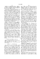
As shown in FIGS. 1 and 2, conventional practices comprise depositing metal layer 11 on dielectric layer 10 which is typically formed on a semiconductor substrate containing an active region with transistors (not shown) After photolithography, etching is then conducted to form a patterned metal layer comprising metal features 11a, 11b, 11c and 11d with gaps therebetween. A dielectric material 12, such as spin on glass (SOG), is typically deposited to fill in the gaps between the metal features, and baked at a temperature of about 300° C. to about 450° C., for a period of time up to about two hours, depending upon the particular SOG material employed, to enhance the dielectric properties of SOG. A layer of silicon dioxide is deposited by plasma enhanced chemical vapor deposition (PECVD) to cap the SOG layer and is subsequently planarized, as by CMP, before the next level of via and metal wiring is attempted.
As feature sizes, e.g., metal lines and interwiring spacings, shrink to 0.25 microns and below, such as 0.18 microns, it becomes increasingly difficult to satisfactorily fill in the interwiring spacings voidlessly and obtain adequate step coverage. Hydrogen silsesquioxane (HSQ) offers many advantages for use in interconnect patterns. HSQ is relatively carbon free, thereby avoiding poison via problems. Moreover, the absence of carbon renders it unnecessary to etch back HSQ below the upper surface of the metal lines to avoid shorting. In addition, HSQ exhibits excellent planarity and is capable of gap filling interwiring spacings less than 0.15 microns employing conventional spin-on equipment. HSQ undergoes a melting phase at approximately 200° C., but does not convert to the high dielectric constant glass phase until reaching temperatures of about 400° C. for intermetal applications and about 700° C. to about 800° C. for premetal applications.
However, after experimental investigation and testing, it was found that the use of HSQ to gap fill the spaces between metal features results in a degradation of the electromigration resistance of the metal feature, e.g., a metal line. Electromigration failure is a serious limitation on the lifetime and reliability of conventional semiconductor devices and is attributed to the conductive interconnection lines. The phenomenon of electromigration involves the flow of electrons causing the migration of atoms, thereby generating voids and hillocks. The formation of voids creates an opening in a conductive interconnection line, thereby decreasing the performance of the interconnection line. The formation of voids generates areas of increased resistance which undesirably reduce the speed of a semiconductor device. Thus, the electromigration phenomenon constitutes a limitation on the lifetime of the conductive interconnection line, as well as the performance of the semiconductor device.
Electromigration in a metal interconnection line can be characterized by the movement of ions induced by a high electrical current density. As miniaturization of the feature size of the semiconductor device increases, the current density also increases and, hence, electromigration induced metallization failures increase. Current metallization failures resulting from electromigration exceed about 30% of the total of metallization failures.
The continuing demand for increased miniaturization requires conductive patterns comprising features, such as conductive lines with interwiring spacings therebetween, having a feature size of about 0.25 microns and under. Semiconductor devices comprising conductive patterns having sub-micron design features are characterized by a high electrical current density and, consequently, increased metallization and electromigration failures. The requirement for a longer electromigration lifetime is of critical importance for an interconnection system.
Prior attempts to restrain electromigration involve the use of overcoating, alloying, or multilevel metallization. In copending application Ser. No. 08/992,953, filed on on Dec. 18, 1997, the electromigration characteristics of metal features are improved by applying a conductive layer to substantially surround and encapsulate the metal features, as by depositing a conductive composite comprising a first layer of titanium and a second layer of titanium-nitride.
There exists a need for semiconductor technology enabling the use of HSQ as a gap fill layer without adversely affecting the electromigration resistance of metal features, such as metal lines. There exists a particular need for semiconductor technology enabling the use of HSQ as a gap fill layer for metal features of about 0.25 microns and under without adversely affecting electromigration resistance.
DISCLOSURE OF THE INVENTION
An object of the present invention is a highly integrated semiconductor device containing an interconnection structure comprising metal features gap filled with HSQ, which interconnection structure exhibits an enhanced electromigration lifetime.
Another object of the present invention is a method of manufacturing a semiconductor device employing HSQ as a gap fill layer without adverse affecting the electromigration existence of the gap filled metal features.
Additional objects, advantages and other features of the invention will be set forth in part in the description which follows and in part will become apparent to those having ordinary skill in the art upon examination of the following or may be learned from the practice of the invention. The objects and advantages of the invention may be realized and obtained as particularly pointed out in the appended claims.
According to the present invention, the foregoing and other objects are achieved in part by a semiconductor device comprising: a dielectric layer; a first patterned metal layer formed on the dielectric layer, the patterned metal layer having metal features with an upper surface and side surfaces and gaps between the metal features; a substantially conformal dielectric layer on the upper surface and side surfaces of the metal features and lining the gaps; and a layer of hydrogen silsesquioxane (HSQ) on the substantially conformal dielectric layer and filling the gaps.
Another aspect of the present invention is a method of manufacturing a semiconductor device, which method comprises: forming a dielectric layer on a substrate; forming a patterned metal layer on the dielectric layer, the patterned metal layer containing metal features having an upper surface and side surfaces and gaps between the metal features; forming a substantially conformal dielectric layer on the upper surface and side surfaces of the metal features and lining the gaps; and forming a layer of hydrogen silsesquioxane (HSQ) on the substantially conformal dielectric layer and filling the gaps.
Additional objects and advantages of the present invention will become readily apparent to those skilled in this art from the following detailed description, wherein only the preferred embodiment of the invention is shown and described, simply by way of illustration of the best mode contemplated for carrying out the invention. As will be realized, the invention is capable of other and different embodiments, and its several details are capable of modifications in various obvious respects, all without departing from the invention. Accordingly, the drawings and description are to be regarded as illustrative in nature, and not as restrictive.
BRIEF DESCRIPTION OF DRAWINGS
FIGS. 1 and 2 schematically illustrate conventional methodology in gap filling a patterned metal layer.
FIG. 3 schematically illustrates an embodiment of the present invention.
DESCRIPTION OF THE INVENTION
The present invention enables the use of HSQ to gap fill, particularly a patterned metal layer comprising metal features, such as metal lines, having a feature size of about 0.25 microns and under, without adverse reduction of the electromigration resistance of the metal features. A limitation on the lifetime and reliability of conventional semiconductor devices attributed to metal interconnections is due to electromigration. The phenomenon of electromigration involves the flow of electrons causing the migration of metal atoms, thereby generating voids and hillocks. The formation of voids creates an opening in a metal layer or line, thereby decreasing performance. The formation of voids generates areas of increased resistance which undesirably reduce the speed at which a semiconductor device can function. Thus, the electromigration phenomenon constitutes a limitation on the lifetime of a metal line as well as the performance of the semiconductor device. In the extreme case, the device becomes non-functional due to a discontinuity in the metal line generated by a sufficiently large void.
Electromigration in a metal interconnection line can be characterized by the movement of ions induced by a high electrical current density. As the feature size of semiconductor devices decreases, the current density consequently increases and, hence, electromigration-induced metallization failures increase. Current metallization failures resulting from electromigration are acutely problematic.
Semiconductor devices comprising conductive patterns having design features of 0.25 microns and under are characterized by a high electrical current density and, consequently, increased metallization electromigration failures. The requirement for a long electromigration lifetime is of critical importance for an interconnection system. The increased susceptibility to electromigration as design features shrink is exacerbated by a reduction in electromigration resistance upon attempting to employ HSQ to gap fill patterned metal layers.
The exact mechanism involved in degradation of the electromigration resistance of metal features, such as metal lines, gap filled with HSQ is not known. However, it is believed that the relative low density or softness of the deposited HSQ gap fill layer renders it undesirably flexible and, hence, susceptible to aluminum extrusion during electromigration. In accordance with the present invention, a thin, substantially conformal dielectric layer is deposited on a patterned metal layer to encapsulate the metal features lining the gaps therebetween. Desirably, the substantially conformal dielectric layer comprises a material having a higher density than that of HSQ. HSQ is then deposited on the substantially conformal dielectric layer gap filling the spaces between the metal features which spaces are lined with a thin layer of the denser conformal dielectric material.
The exact mechanism involved in preventing the degradation of the metal features contain a conformal dielectric lining in accordance with the present invention prior to gap filling with HSQ is not known with certainty. However, electromigration occurs primarily along metal grain boundaries wherein the activation energy is the least. It is, therefore, believed that initially encapsulating the patterned metal features with a relatively dense dielectric material serves to freeze the grain boundaries, thereby preventing grain boundary movement and growth, which significantly improves the electromigration characteristics of the patterned metal features.
In the various embodiments of the present invention, the substantially conformal dielectric layer can comprise any of various dielectric materials which exhibits a density sufficiently greater than HSQ to prevent a reduction in electromigration resistance of metal features, such as an oxide, a nitride, oxynitride or silicon oxime. In preferred embodiments of the present invention, a substantially conformal oxide layer is deposited to encapsulate the patterned metal features, since oxides generally exhibit a lower dielectric constant than nitrides or oxynitrides. By employing an oxide having a relatively low dielectric constant, capacitive coupling between conductive lines is reduced, thereby enhancing circuit speed.
In a preferred embodiment of the present invention, a high density plasma (HDP) oxide is deposited as the conformal dielectric liner prior to deposition of HSQ as a gap filling layer. HDP oxide is typically deposited by high density plasma chemical vapor deposition (HDP-CVD). See, for example, Liu et al., "Integrated HDP Technology for Sub-0.25 Micron Gap Fill", pp. 618-619; Bothra et al., "INTEGRATION OF 0.25 μm THREE AND FIVE LEVEL INTERCONNECT SYSTEM FOR HIGH PERFORMANCE ASIC.", pp. 43-48; Wang et al., "Process Window Characterization of ULTIMA HDP-CVDFM USG Film", pp. 405-408; Saikawa et al., "High Density Plasma CVD for 0.3 μm Device Application", pp. 69-75; Nguyen et al., "CHARACTERIZATION OF HIGH DENSITY PLASMA DEPOSITED SILICON OXIDE DIELECTRIC FOR 0.25 MICRON ULSI", pp. 69-74; all of which papers were presented at the Jun. 10-12, 1997 VMIC Conference, 1997 ISMIC.
HDP oxide easily fills gaps in a patterned metal layer with a 0.25 micron design rule. HDP oxide is relatively dense and exhibits high chemical stability and etch resistance. Advantageously, HDP oxide can be deposited as a thin conformal layer, having a thickness of about 100 Å to about 1,000 Å, encapsulating metal features having a feature size of about 0.25 microns which are typically formed with an interwiring spacing of about 0.375 microns.
An embodiment of the present invention is schematically illustrated in FIG. 3 and comprises metal features 31 formed on dielectric layer 30. Metal features 31 can be formed consistent with conventional practices and typically comprise a first lower metal layer 31A of a refractory metal, such as tungsten or titanium, an intermediate primary conductive layer 31B, such as aluminum or an aluminum alloy, and an upper anti-reflective coating 31C, such as titanium nitride. A relatively high density substantially conformal dielectric layer 32 is then deposited encapsulating metal features 31 and lining the gaps therebetween. In a preferred embodiment, conformal dielectric layer 32 comprises high density plasma oxide deposited by HDP chemical vapor deposition. After depositing the conformal dielectric liner 32, HSQ gap fill layer 33 is deposited on conformal dielectric layer 32, filling the gaps and covering the encapsulated metal features.
The present invention enables the use of HSQ as a gap fill layer without adversely affecting the electromigration resistance of the patterned metal features by depositing a relatively dense substantially conformal dielectric liner encapsulating the metal features prior to HDP deposition. The present invention is applicable to the production of various types of semiconductive devices, particularly high density multi-metal patterned layers with submicron features, particularly submicron features of 0.25 microns and below, exhibiting high speed characteristics and improved reliability. The present invention enables the advantageous use of HSQ to gap fill patterned metal layers without an attendant decrease in electromigration resistance. The present invention is cost effective and can easily be integrated into conventional processing and equipment.
In carrying out the embodiments of the present invention, the metal layers can be formed of any metal typically employed in manufacturing semiconductor devices, such as aluminum, aluminum alloys, copper, copper alloys, gold, gold alloys, silver, silver alloys, refractory metals, refractory metal alloys, and refractory metal compounds. The metal layers of the present invention can be formed by any technique conventionally employed in the manufacture of semiconductor devices. For example, the metal layers can be formed by conventional metallization techniques, such as various types of CVD and sputtering processes, including low pressure chemical vapor deposition (LPCVD), collimated physical vapor deposition (COLPVD), and ionized-metal physical vapor deposition (IMPVD). Normally, when high melting metal point metals such as tungsten are deposited, CVD techniques are employed. Low melting point metals, such as aluminum and aluminum-base alloys, including aluminum-copper alloys, can also be deposited by melting, sputtering, or physical vapor deposition (PVD).
In the previous descriptions, numerous specific details are set forth, such as specific materials, structures, chemicals, processes, etc., in order to provide a thorough understanding of the present invention. However, the present invention can be practiced without resorting to the details specifically set forth. In other instances, well known processing structures have not been described in detail in order not to unnecessarily obscure the present invention.
Only the preferred embodiment of the invention and an example of its versatility are shown and described in the present disclosure. It is to be understood that the invention is capable of use in various other combinations and environments and is capable of changes or modifications within the scope of the inventive concept as expressed herein.

Claims (7)

What is claimed is:
1. A semiconductor device comprises:
a dielectric layer;
a first patterned metal layer formed on the dielectric layer, the patterned metal layer having metal features with an upper surface and side surfaces and gaps between the metal features;
a substantially conformal dielectric layer on the upper surface and side surfaces of the metal features and lining the gaps; and
a layer of hydrogen silsesquioxane (HSQ) on the substantially conformal dielectric layer and filling the gaps, wherein the conformal dielectric layer comprises a material having a density greater than that of HSQ.
2. The semiconductor device according to claim 1, wherein the substantially conformal dielectric layer comprises an oxide liner.
3. The semiconductor device according to claim 2, wherein the oxide liner has a thickness of about 100 Å to about 1,000 Å.
4. The semiconductor device according to claim 3, wherein the substantially conformal oxide layer comprises a high density plasma silicon oxide.
5. The semiconductor device according to claim 1, wherein the metal layer is a composite comprising:
a lower refractory layer;
an intermediate primary conductive layer containing aluminum or an aluminum alloy; and
an upper anti-reflective coating.
6. The semiconductor device according to claim 1, wherein the metal features comprise metal lines having a width no greater than about 0.25 microns and the gaps comprise interwiring spacings no greater than about 0.375 microns.
7. A semiconductor device according to claim 1, wherein the conformal dielectric layer comprises a material selected from the group consisting of oxides, nitrides, oxynitrides and silicon oxime.
US08/993,051 1997-12-18 1997-12-18 Electromigration resistant patterned metal layer gap filled with HSQ Expired - Lifetime US6034420A (en)

Priority Applications (2)

Application Number Priority Date Filing Date Title
US08/993,051 US6034420A (en) 1997-12-18 1997-12-18 Electromigration resistant patterned metal layer gap filled with HSQ
US09/415,218 US6100179A (en) 1997-12-18 1999-10-12 Electromigration resistant patterned metal layer gap filled with HSQ

Applications Claiming Priority (1)

Application Number Priority Date Filing Date Title
US08/993,051 US6034420A (en) 1997-12-18 1997-12-18 Electromigration resistant patterned metal layer gap filled with HSQ

Related Child Applications (1)

Application Number Title Priority Date Filing Date
US09/415,218 Division US6100179A (en) 1997-12-18 1999-10-12 Electromigration resistant patterned metal layer gap filled with HSQ

Publications (1)

Publication Number Publication Date
US6034420A true US6034420A (en) 2000-03-07

Family

ID=25539037

Family Applications (2)

Application Number Title Priority Date Filing Date
US08/993,051 Expired - Lifetime US6034420A (en) 1997-12-18 1997-12-18 Electromigration resistant patterned metal layer gap filled with HSQ
US09/415,218 Expired - Lifetime US6100179A (en) 1997-12-18 1999-10-12 Electromigration resistant patterned metal layer gap filled with HSQ

Family Applications After (1)

Application Number Title Priority Date Filing Date
US09/415,218 Expired - Lifetime US6100179A (en) 1997-12-18 1999-10-12 Electromigration resistant patterned metal layer gap filled with HSQ

Country Status (1)

Country Link
US (2) US6034420A (en)

Cited By (6)

* Cited by examiner, † Cited by third party
Publication number Priority date Publication date Assignee Title
US6127238A (en) * 1999-03-11 2000-10-03 Chartered Semiconductor Manufacturing Ltd. Plasma enhanced chemical vapor deposited (PECVD) silicon nitride barrier layer for high density plasma chemical vapor deposited (HDP-CVD) dielectric layer
US6225210B1 (en) * 1998-12-09 2001-05-01 Advanced Micro Devices, Inc. High density capping layers with improved adhesion to copper interconnects
US6232243B1 (en) * 1997-03-31 2001-05-15 Micron Technology, Inc. Interconnect having recessed contact members with penetrating blades for testing semiconductor dice and packages with contact bumps
US6437441B1 (en) * 1997-07-10 2002-08-20 Kawasaki Microelectronics, Inc. Wiring structure of a semiconductor integrated circuit and a method of forming the wiring structure
US20030207558A1 (en) * 2002-05-06 2003-11-06 Taiwan Semiconductor Manufacturing Co., Ltd. Method forming copper containing semiconductor features to prevent thermally induced defects
US20040026693A1 (en) * 2002-08-07 2004-02-12 International Business Machines Corporation Test structure for locating electromigration voids in dual damascene interconnects

Families Citing this family (5)

* Cited by examiner, † Cited by third party
Publication number Priority date Publication date Assignee Title
US6303525B1 (en) * 2000-08-18 2001-10-16 Philips Electronics No. America Corp. Method and structure for adhering MSQ material to liner oxide
US6645864B1 (en) 2002-02-05 2003-11-11 Taiwan Semiconductor Manufacturing Company Physical vapor deposition of an amorphous silicon liner to eliminate resist poisoning
US20090099566A1 (en) * 2007-10-10 2009-04-16 Maness Megan A Modular stem inserter
US9893159B2 (en) * 2014-08-15 2018-02-13 Taiwan Semiconductor Manufacturing Co., Ltd. Transistor, integrated circuit and method of fabricating the same
US9985026B2 (en) 2014-08-15 2018-05-29 Taiwan Semiconductor Manufacturing Co., Ltd. Transistor, integrated circuit and method of fabricating the same

Citations (8)

* Cited by examiner, † Cited by third party
Publication number Priority date Publication date Assignee Title
US5101259A (en) * 1987-07-31 1992-03-31 Kabushiki Kaisha Toshiba Semiconductor device and manufacturing method thereof
US5589712A (en) * 1993-12-03 1996-12-31 Ricoh Company, Ltd. Semiconductor integrated circuit device and a method of manufacturing the same
US5670823A (en) * 1992-06-15 1997-09-23 Kruger; James B. Integrated circuit barrier structure
US5675186A (en) * 1994-05-31 1997-10-07 Advanced Micro Devices, Inc. Construction that prevents the undercut of interconnect lines in plasma metal etch systems
US5708303A (en) * 1994-09-15 1998-01-13 Texas Instruments Incorporated Semiconductor device having damascene interconnects
US5780908A (en) * 1995-05-09 1998-07-14 Matsushita Electric Industrial Co., Ltd. Semiconductor apparatus with tungstein nitride
US5786625A (en) * 1994-09-14 1998-07-28 Yamaha Corporation Moisture resistant semiconductor device
US5847459A (en) * 1994-08-31 1998-12-08 Fujitsu Limited Multi-level wiring using refractory metal

Family Cites Families (3)

* Cited by examiner, † Cited by third party
Publication number Priority date Publication date Assignee Title
US6008540A (en) * 1997-05-28 1999-12-28 Texas Instruments Incorporated Integrated circuit dielectric and method
US5888898A (en) * 1997-10-23 1999-03-30 Advanced Micro Devices, Inc. HSQ baking for reduced dielectric constant
US5936307A (en) * 1997-11-12 1999-08-10 Advanced Micro Devices, Inc. Surface modification method for film stress reduction

Patent Citations (8)

* Cited by examiner, † Cited by third party
Publication number Priority date Publication date Assignee Title
US5101259A (en) * 1987-07-31 1992-03-31 Kabushiki Kaisha Toshiba Semiconductor device and manufacturing method thereof
US5670823A (en) * 1992-06-15 1997-09-23 Kruger; James B. Integrated circuit barrier structure
US5589712A (en) * 1993-12-03 1996-12-31 Ricoh Company, Ltd. Semiconductor integrated circuit device and a method of manufacturing the same
US5675186A (en) * 1994-05-31 1997-10-07 Advanced Micro Devices, Inc. Construction that prevents the undercut of interconnect lines in plasma metal etch systems
US5847459A (en) * 1994-08-31 1998-12-08 Fujitsu Limited Multi-level wiring using refractory metal
US5786625A (en) * 1994-09-14 1998-07-28 Yamaha Corporation Moisture resistant semiconductor device
US5708303A (en) * 1994-09-15 1998-01-13 Texas Instruments Incorporated Semiconductor device having damascene interconnects
US5780908A (en) * 1995-05-09 1998-07-14 Matsushita Electric Industrial Co., Ltd. Semiconductor apparatus with tungstein nitride

Non-Patent Citations (10)

* Cited by examiner, † Cited by third party
Title
Bothra et al., "Integration of 0.25μm Three and Five Level Interconnect System for High Performance ASIC," Jun. 10-12, 1997, VMIC Conference, 1997, ISMIC-107/97/0043, pp. 43-48.
Bothra et al., Integration of 0.25 m Three and Five Level Interconnect System for High Performance ASIC, Jun. 10 12, 1997, VMIC Conference, 1997, ISMIC 107/97/0043, pp. 43 48. *
Liu et al., "Integrated HDP Technology for Sub-0.25 Micron Gap Fill," Jun. 10-12, 1997, VMIC Conference, 1997, ISMIC-107/97/0618(c), pp. 618-619.
Liu et al., Integrated HDP Technology for Sub 0.25 Micron Gap Fill, Jun. 10 12, 1997, VMIC Conference, 1997, ISMIC 107/97/0618(c), pp. 618 619. *
Nguyen et al., "Characterization of High Density Plasma Deposited Silicon Oxide Dielectric for 0.25 Micron ULSI," Jun. 27-29, 1995, VMIC Conference 1995 ISMIC-104/95/0069, pp. 69-74.
Nguyen et al., Characterization of High Density Plasma Deposited Silicon Oxide Dielectric for 0.25 Micron ULSI, Jun. 27 29, 1995, VMIC Conference 1995 ISMIC 104/95/0069, pp. 69 74. *
Saikawa et al., "High Density Plasma CVD for 0.3μm Device Application," Jun. 18-20, 1996, VMIC Conference 1996 ISMIC-106/96/0069(c), pp. 69-75.
Saikawa et al., High Density Plasma CVD for 0.3 m Device Application, Jun. 18 20, 1996, VMIC Conference 1996 ISMIC 106/96/0069(c), pp. 69 75. *
Wang et al., "Process Window Characterization of Ultima HDP-CVD™ USG Film," Feb. 10-11, 1997, DUMIC Conference 1997 ISMIC-222D/97/0405, pp. 405-408, 619.
Wang et al., Process Window Characterization of Ultima HDP CVD USG Film, Feb. 10 11, 1997, DUMIC Conference 1997 ISMIC 222D/97/0405, pp. 405 408, 619. *

Cited By (7)

* Cited by examiner, † Cited by third party
Publication number Priority date Publication date Assignee Title
US6232243B1 (en) * 1997-03-31 2001-05-15 Micron Technology, Inc. Interconnect having recessed contact members with penetrating blades for testing semiconductor dice and packages with contact bumps
US6437441B1 (en) * 1997-07-10 2002-08-20 Kawasaki Microelectronics, Inc. Wiring structure of a semiconductor integrated circuit and a method of forming the wiring structure
US6225210B1 (en) * 1998-12-09 2001-05-01 Advanced Micro Devices, Inc. High density capping layers with improved adhesion to copper interconnects
US6127238A (en) * 1999-03-11 2000-10-03 Chartered Semiconductor Manufacturing Ltd. Plasma enhanced chemical vapor deposited (PECVD) silicon nitride barrier layer for high density plasma chemical vapor deposited (HDP-CVD) dielectric layer
US20030207558A1 (en) * 2002-05-06 2003-11-06 Taiwan Semiconductor Manufacturing Co., Ltd. Method forming copper containing semiconductor features to prevent thermally induced defects
US20040026693A1 (en) * 2002-08-07 2004-02-12 International Business Machines Corporation Test structure for locating electromigration voids in dual damascene interconnects
US6995392B2 (en) 2002-08-07 2006-02-07 International Business Machines Corporation Test structure for locating electromigration voids in dual damascene interconnects

Also Published As

Publication number Publication date
US6100179A (en) 2000-08-08

Similar Documents

Publication Publication Date Title
US6627539B1 (en) Method of forming dual-damascene interconnect structures employing low-k dielectric materials
EP1029344B1 (en) Method of forming hsq layers and borderless vias with hsq gap filled patterned metal layers
US6143641A (en) Structure and method for controlling copper diffusion and for utilizing low K materials for copper interconnects in integrated circuit structures
US7132363B2 (en) Stabilizing fluorine etching of low-k materials
US6100184A (en) Method of making a dual damascene interconnect structure using low dielectric constant material for an inter-level dielectric layer
EP0761014B1 (en) Simplified dual damascene process for multilevel metallization and interconnection structure
US6573606B2 (en) Chip to wiring interface with single metal alloy layer applied to surface of copper interconnect
US6245663B1 (en) IC interconnect structures and methods for making same
US6004188A (en) Method for forming copper damascene structures by using a dual CMP barrier layer
US6445073B1 (en) Damascene metallization process and structure
US6573572B2 (en) Damascene structure and method of making
US6232221B1 (en) Borderless vias
US6753249B1 (en) Multilayer interface in copper CMP for low K dielectric
US6034420A (en) Electromigration resistant patterned metal layer gap filled with HSQ
US6046106A (en) High density plasma oxide gap filled patterned metal layers with improved electromigration resistance
US6218282B1 (en) Method of forming low dielectric tungsten lined interconnection system
US6084290A (en) HSQ dielectric interlayer
US6501180B1 (en) Structure and method for controlling copper diffusion and for utilizing low K materials for copper interconnects in integrated circuit structures
US5942801A (en) Borderless vias with HSQ gap filled metal patterns having high etching resistance
US5958798A (en) Borderless vias without degradation of HSQ gap fill layers
US6638849B2 (en) Method for manufacturing semiconductor devices having copper interconnect and low-K dielectric layer
US5888911A (en) HSQ processing for reduced dielectric constant
US6048796A (en) Method of manufacturing multilevel metal interconnect
US5888898A (en) HSQ baking for reduced dielectric constant
US6043147A (en) Method of prevention of degradation of low dielectric constant gap-fill material

Legal Events

Date Code Title Description
AS Assignment

Owner name: ADVANCED MICRO DEVICES, INC., CALIFORNIA

Free format text: ASSIGNMENT OF ASSIGNORS INTEREST;ASSIGNOR:TRAN, KHANH;REEL/FRAME:009218/0647

Effective date: 19980520

STCF Information on status: patent grant

Free format text: PATENTED CASE

FPAY Fee payment

Year of fee payment: 4

FPAY Fee payment

Year of fee payment: 8

AS Assignment

Owner name: AMD TECHNOLOGIES HOLDINGS, INC., CALIFORNIA

Free format text: ASSIGNMENT OF ASSIGNORS INTEREST;ASSIGNOR:ADVANCED MICRO DEVICES, INC.;REEL/FRAME:022764/0488

Effective date: 20090302

Owner name: GLOBALFOUNDRIES INC., CAYMAN ISLANDS

Free format text: ASSIGNMENT OF ASSIGNORS INTEREST;ASSIGNOR:AMD TECHNOLOGIES HOLDINGS, INC.;REEL/FRAME:022764/0544

Effective date: 20090302

FPAY Fee payment

Year of fee payment: 12

AS Assignment

Owner name: GLOBALFOUNDRIES U.S. INC., NEW YORK

Free format text: RELEASE BY SECURED PARTY;ASSIGNOR:WILMINGTON TRUST, NATIONAL ASSOCIATION;REEL/FRAME:056987/0001

Effective date: 20201117