US6038150A - Transistorized rectifier for a multiple output converter - Google Patents
Transistorized rectifier for a multiple output converter Download PDFInfo
- Publication number
- US6038150A US6038150A US09/039,018 US3901898A US6038150A US 6038150 A US6038150 A US 6038150A US 3901898 A US3901898 A US 3901898A US 6038150 A US6038150 A US 6038150A
- Authority
- US
- United States
- Prior art keywords
- transistor
- voltage
- recited
- voltage potential
- converter circuit
- Prior art date
- Legal status (The legal status is an assumption and is not a legal conclusion. Google has not performed a legal analysis and makes no representation as to the accuracy of the status listed.)
- Expired - Lifetime
Links
Images


Classifications
-
- H—ELECTRICITY
- H02—GENERATION; CONVERSION OR DISTRIBUTION OF ELECTRIC POWER
- H02M—APPARATUS FOR CONVERSION BETWEEN AC AND AC, BETWEEN AC AND DC, OR BETWEEN DC AND DC, AND FOR USE WITH MAINS OR SIMILAR POWER SUPPLY SYSTEMS; CONVERSION OF DC OR AC INPUT POWER INTO SURGE OUTPUT POWER; CONTROL OR REGULATION THEREOF
- H02M3/00—Conversion of dc power input into dc power output
- H02M3/22—Conversion of dc power input into dc power output with intermediate conversion into ac
- H02M3/24—Conversion of dc power input into dc power output with intermediate conversion into ac by static converters
- H02M3/28—Conversion of dc power input into dc power output with intermediate conversion into ac by static converters using discharge tubes with control electrode or semiconductor devices with control electrode to produce the intermediate ac
- H02M3/325—Conversion of dc power input into dc power output with intermediate conversion into ac by static converters using discharge tubes with control electrode or semiconductor devices with control electrode to produce the intermediate ac using devices of a triode or a transistor type requiring continuous application of a control signal
- H02M3/335—Conversion of dc power input into dc power output with intermediate conversion into ac by static converters using discharge tubes with control electrode or semiconductor devices with control electrode to produce the intermediate ac using devices of a triode or a transistor type requiring continuous application of a control signal using semiconductor devices only
- H02M3/33561—Conversion of dc power input into dc power output with intermediate conversion into ac by static converters using discharge tubes with control electrode or semiconductor devices with control electrode to produce the intermediate ac using devices of a triode or a transistor type requiring continuous application of a control signal using semiconductor devices only having more than one ouput with independent control
-
- H—ELECTRICITY
- H02—GENERATION; CONVERSION OR DISTRIBUTION OF ELECTRIC POWER
- H02M—APPARATUS FOR CONVERSION BETWEEN AC AND AC, BETWEEN AC AND DC, OR BETWEEN DC AND DC, AND FOR USE WITH MAINS OR SIMILAR POWER SUPPLY SYSTEMS; CONVERSION OF DC OR AC INPUT POWER INTO SURGE OUTPUT POWER; CONTROL OR REGULATION THEREOF
- H02M3/00—Conversion of dc power input into dc power output
- H02M3/22—Conversion of dc power input into dc power output with intermediate conversion into ac
- H02M3/24—Conversion of dc power input into dc power output with intermediate conversion into ac by static converters
- H02M3/28—Conversion of dc power input into dc power output with intermediate conversion into ac by static converters using discharge tubes with control electrode or semiconductor devices with control electrode to produce the intermediate ac
- H02M3/325—Conversion of dc power input into dc power output with intermediate conversion into ac by static converters using discharge tubes with control electrode or semiconductor devices with control electrode to produce the intermediate ac using devices of a triode or a transistor type requiring continuous application of a control signal
- H02M3/335—Conversion of dc power input into dc power output with intermediate conversion into ac by static converters using discharge tubes with control electrode or semiconductor devices with control electrode to produce the intermediate ac using devices of a triode or a transistor type requiring continuous application of a control signal using semiconductor devices only
- H02M3/33569—Conversion of dc power input into dc power output with intermediate conversion into ac by static converters using discharge tubes with control electrode or semiconductor devices with control electrode to produce the intermediate ac using devices of a triode or a transistor type requiring continuous application of a control signal using semiconductor devices only having several active switching elements
- H02M3/33576—Conversion of dc power input into dc power output with intermediate conversion into ac by static converters using discharge tubes with control electrode or semiconductor devices with control electrode to produce the intermediate ac using devices of a triode or a transistor type requiring continuous application of a control signal using semiconductor devices only having several active switching elements having at least one active switching element at the secondary side of an isolation transformer
Definitions
- the present invention generally relates to power converters, and, more particularly, to multiple output converters.
- the primary output subcircuit for generating power at output terminal #1 includes a secondary coil 10 that is responsive to a primary coil 21 for generating a voltage/current that passes through a diode 12 and a capacitor 14.
- a feedback line 16 from output terminal #1 is connected to the primary PWM control circuit 18 through an isolation unit 19.
- the primary PWM control circuit 18 detects the level of the feedback signal and correspondingly adjusts the fluctuation of the voltage to the control gate of the transistor 17 where the transistor is turned on and off, thereby adjusting the fluctuation of the current going through the primary coil 21.
- the fluctuation of the current going through the coil 21 causes the primary coil 21 to generate a magnetic field having an intensity that corresponds to the frequency of the current fluctuation.
- the magnetic field in turn affects the secondary coil 10 and causes the secondary coil 10 to generate a voltage/current at output terminal #1 of the primary output subcircuit (via the diode).
- the secondary subcircuit for generating a voltage/current at output terminal #2 comprises a secondary coil 22 responding to the primary coil in generating a voltage/current that passes through a diode 24 and a capacitor 26 where the output at output terminal #2 is regulated by a linear drop regulator 16. While the use of linear regulators are fairly simple, their use is limited to low current outputs because of the relatively low efficiency of the linear regulators. Note that there can be more than one secondary subcircuits for generating different voltages.
- the secondary subcircuit 30 generally comprises a secondary coil 31 for generating a voltage/current that passes through a magamp 32, a diode 34, and a capacitor 36.
- a magamp control circuit 38 senses the voltage level at output terminal #2 and generates a control signal to node 37 to cause the subcircuit to produce the overall and desired output. While this type of circuit is suitable for high current outputs, it is difficult to control the output when the load current is low. Also, it is a relatively complex circuit when compared to a semiconductor switch.
- a secondary converter subcircuit comprises a secondary coil 42 for generating a voltage/current that passes through a diode 44, transistor M1, and a capacitor 48.
- a SSPR ASIC 50 sensing the voltage/current levels between two points (output terminal #2 and the sync node), generates a control signal to the gate terminal of a transistor M1 to control the voltage level generated at output terminal #2.
- the SSPR circuit has a simpler design than that of the magamp and provides better efficiency than that of a linear regulator.
- SSPR PWM ASIC can significantly improve converter efficiency and simplify the converter design process.
- a converter using a SSPR/MOSFET combination is no more efficient than a converter using a magamp.
- a magamp is a more efficient switch than a SSPR/MOSFET switch.
- a presently preferred embodiment of the present invention uses and operates a transistor to prevent reverse conduction of the current in the secondary subcircuit of a converter circuit.
- the diode in the secondary subcircuits of the prior art is replaced by a transistor and the circuitry for controlling the transistor is made part of the control circuit (ASIC).
- the secondary subcircuit includes a secondary coil 60 for generating a voltage that passes through a first transistor M1, a capacitor 62, and a second transistor M2, where the output of the secondary subcircuit is generated at output terminal #2.
- a presently preferred embodiment of a control circuit 64 detects the subcircuit output level at the sync node and at output terminal #2 and controls transistors M1 and M2 accordingly in generating the desired output at output terminal #2.
- An advantage of the present invention is that it provides a converter subcircuit that does not require a diode.
- Another advantage of the present invention is that it provides a diodeless converter subcircuit using a transistor to prevent reverse conduction.
- Yet another advantage of the present invention is that it provides a diodeless converter using a transistor where the body diode of the transistor is used to detect the presence of any current flowing through the transistor.
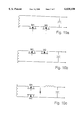
- FIG. 1 illustrates a prior art flyback converter having a primary subcircuit and a secondary subcircuit where the secondary subcircuit uses a linear drop regulator to regulate the voltage level generated at output terminal #2;
- FIG. 2 illustrates a prior art flyback converter having a primary subcircuit and a secondary subcircuit where the secondary subcircuit uses a magamp and magamp control circuit to regulate the voltage level generated at output terminal #2;
- FIG. 3 illustrates a prior art flyback converter having a primary subcircuit and a secondary subcircuit where the secondary subcircuit uses a transistor controlled by a secondary side post regulator in regulating the voltage level generated at output terminal #2;
- FIG. 4 illustrates a converter circuit having a primary subcircuit and a secondary subcircuit where the secondary subcircuit uses a transistor controlled by a diode-less secondary side post regulator in regulating the voltage level generated at output terminal #2;
- FIGS. 5a-5g juxtapose a series of timing diagrams to illustrate timing relationships for various voltages
- FIG. 6 is a flow chart illustrating the logic for predicting and controlling the turning on and off of the transistor to prevent reverse conduction
- FIGS. 7a-7c illustrate timing diagrams for the diode-less prediction circuit
- FIG. 8 shows an aspect in the regulation of the output voltage
- FIG. 9 shows the voltage timing relationship between the primary switch and Vgs for transistor M1.
- FIGS. 10a-10c illustrate alternative converter circuits.
- a presently preferred embodiment of the present invention provides a novel circuit for diode-less secondary side post regulation (DL-SSPR).
- DL-SSPR diode-less secondary side post regulation
- the secondary subcircuit includes a secondary coil 60 for generating a current/voltage that passes through a first transistor M1, a capacitor 62, and a second transistor M2, where the output of the secondary subcircuit is generated at output terminal #2.
- a presently preferred embodiment of a control circuit 64 detects the subcircuit output level at the sync node and at output terminal #2 and controls transistors M1 and M2 accordingly in generating the desired output at output terminal #2.
- FIGS. 5a-5g the timing diagrams of the relevant voltage levels and current levels are illustrated to provide a better understanding of the methods of the preferred embodiment of the present invention.
- FIG. 5a illustrates the ideal voltage wave form, Vgs, for the primary switch, which is a square wave form generated by the primary PWM control circuit on the primary side.
- FIG. 5b illustrates one ideal logical synchronization voltage wave form. In this case, it is a square wave that is complementary to the square wave generated by the primary switch.
- FIG. 5c the timing diagram of the current going through the diode is illustrated by FIG. 5c.
- FIG. 5d illustrates the voltage wave form using conventional control methods, where the M2 transistor is turned off only after detecting that there that is not a forward current (or positive voltage) and that the current has reversed in direction (or negative voltage).
- the delay in turning off the M2 transistor in time would result in the discharge of current from the capacitor where the discharge is shown by the downward current spike illustrated in FIG. 5e.
- FIG. 5f illustrates the desired Vgs timing diagram for transistor M2 (which is also the Vgs timing generated by the presently preferred embodiment).
- the circuit of the preferred embodiment must be able to predict primary switch timing and turn transistor M2 off before the primary switch turns on.
- primary switch timing for the last time period is used in conjunction with the body diode of (or an external diode for) transistor M2.
- a ramp voltage, Vramp having an upward slope corresponding to the situation when coil energy is being discharged to the load, is generated, and Vramp is also produced as a function of Vsyn where Vsyn is complementary to Vgs for the primary switch.
- the generating of the ramp voltage is in relation with the on and off timing of the primary switch and is not limited to a particular shape or form.
- FIG. 6 illustrates the flow chart for determining the timing control for transistor M2.
- Transistor M2 is turned off when Vramp is greater than a reference voltage (Vref) 70.
- the reference voltage is initially set to zero volt and is used as a reference voltage point.
- transistor M2 can be programmed to be turned off immediately after it was turned on or can simply remain off for the first few cycles.
- the voltage across the body diode of transistor M2 is detected.
- transistor M2 body diode conducts and Vds is at a forward body diode voltage that may be -0.6 volt or otherwise, depending on the device. This body diode voltage is detected and Vref is upwardly adjusted accordingly. If Vds equals the forward body diode voltage for a time period greater than a first predefined time period, Vref is step increased a first predetermined amount 76.
- the predefined time period is set at 100 ns. If Vds equals the forward body diode voltage for a time period less than a second predefined time period, Vref is step decreased a second predetermined amount 74. In the next cycle, transistor M2 is turned on when Vsync is less than 0 volt. This detection and adjustment process repeat in a continuous loop.
- FIGS. 7a-7c illustrate Vref and Vramp in accordance with the detected voltage level of the body diode of transistor M2 and the duration of such voltage level. More specifically, FIG. 7a illustrates Vgs for transistor M2, FIG. 7b illustrates Vds for transistor M2, and FIG. 7c illustrates the ramp voltage, Vramp, and the reference voltage, Vref. As is illustrated by FIG. 7c, when Vref intersects Vramp at the intersection indicated at 82, Vgs is turned off to prevent reverse conduction.
- Vref When body diode conduction caused by transistor M2 being turned off at a time that is greater than a predefined period of time (100 ns), Vref would be upwardly adjusted such that Vref would intersect Vramp at a later point in time and transistor M2 would be turned off at a later point in time to minimize or prevent body diode conduction.
- the time period is less than the predefined period of time, e.g. the time period less than 20 ns, Vref would be downwardly adjusted so that transistor M2 is turned off earlier in time to prevent reverse conduction.
- Transistor M2 is turned on when Vsync is less than zero.
- transistor M1 operates as the PWM switch for the secondary subcircuit and is controlled by the DL-SSPR control circuit (FIG. 4, 64) to regulate the converter output voltage.
- the primary switch After the primary switch is turned off, the mutual inductance discharges its energy to the converter output (load).
- the DL-SSPR uses transistor M1's on-time/off-time ratio to regulate the output voltage.
- the primary switch on-time is indicated at 90
- transistor M1 on-time is indicated at 92.
- transistor M1 is turned on (as indicated at 98) by the DL-SSPR control circuit when the primary switch is on.
- FIGS. 10a, 10b, and 10c illustrates certain ones of the alternative secondary subcircuit variations in the arrangement of the circuit components. More specifically, FIG. 10a illustrates a coil for generating a voltage potential and a corresponding current to pass through a capacitor, transistors M1 and M2, and back to the coil. FIG. 10b illustrates a coil for generating a voltage potential and a corresponding current to pass through to transistors M1 and M2, a capacitor, and back to the coil. FIG.
- 10c shows a coil for generating a voltage potential and corresponding current that passes through transistor M1, an inductor, a capacitor, transistor M2, and back to the coil; a diode is disposed at one terminal between transistor M1 and the inductor and at another terminal between transistor M2 and the capacitor.
Abstract
Description
Claims (34)
Priority Applications (1)
| Application Number | Priority Date | Filing Date | Title |
|---|---|---|---|
| US09/039,018 US6038150A (en) | 1997-07-23 | 1998-03-13 | Transistorized rectifier for a multiple output converter |
Applications Claiming Priority (2)
| Application Number | Priority Date | Filing Date | Title |
|---|---|---|---|
| US5348797P | 1997-07-23 | 1997-07-23 | |
| US09/039,018 US6038150A (en) | 1997-07-23 | 1998-03-13 | Transistorized rectifier for a multiple output converter |
Publications (1)
| Publication Number | Publication Date |
|---|---|
| US6038150A true US6038150A (en) | 2000-03-14 |
Family
ID=21984610
Family Applications (1)
| Application Number | Title | Priority Date | Filing Date |
|---|---|---|---|
| US09/039,018 Expired - Lifetime US6038150A (en) | 1997-07-23 | 1998-03-13 | Transistorized rectifier for a multiple output converter |
Country Status (2)
| Country | Link |
|---|---|
| US (1) | US6038150A (en) |
| JP (1) | JP3445497B2 (en) |
Cited By (55)
| Publication number | Priority date | Publication date | Assignee | Title |
|---|---|---|---|---|
| US6297970B2 (en) * | 1999-12-10 | 2001-10-02 | International Business Machines Corporation | Multiple output synchronous rectifier circuit providing zero volt switch mode operation |
| WO2001078223A1 (en) * | 2000-04-07 | 2001-10-18 | Telefonaktiebolaget Lm Ericsson (Publ) | Method and arrangement for regulating low output voltages in multiple output flyback dc/dc converters |
| US6356060B1 (en) * | 1998-05-29 | 2002-03-12 | Stmicroelectronics S.A. | Switching circuit and method for use in a switching circuit |
| US6449175B1 (en) * | 2000-08-11 | 2002-09-10 | Astec International Limited | Switched magamp post regulator |
| WO2002077629A1 (en) * | 2001-03-26 | 2002-10-03 | Proteome Systems Intellectual Property Pty Ltd | Electrophoresis apparatus incorporating multi-channel power supply |
| US20050122753A1 (en) * | 2003-11-04 | 2005-06-09 | International Rectifier Corporation | Integrated synchronous rectifier package |
| US20060209754A1 (en) * | 2005-03-16 | 2006-09-21 | Ji Tingfang | Channel structures for a quasi-orthogonal multiple-access communication system |
| US20060223449A1 (en) * | 2005-04-01 | 2006-10-05 | Qualcomm Incorporated | Systems and methods for control channel signaling |
| US20070041226A1 (en) * | 2005-08-17 | 2007-02-22 | Adc Dsl Systems, Inc. | Secondary regulation in a multiple output flyback topology |
| US20070047485A1 (en) * | 2005-08-24 | 2007-03-01 | Qualcomm Incorporated | Varied transmission time intervals for wireless communication system |
| US20070060178A1 (en) * | 2005-08-22 | 2007-03-15 | Alexei Gorokhov | Segment sensitive scheduling |
| US20070097909A1 (en) * | 2005-10-27 | 2007-05-03 | Aamod Khandekar | Scalable frequency band operation in wireless communication systems |
| US20070098050A1 (en) * | 2005-10-27 | 2007-05-03 | Aamod Khandekar | Pilot symbol transmission in wireless communication systems |
| US20070244510A1 (en) * | 2006-04-14 | 2007-10-18 | Ethicon Endo-Surgery, Inc. | Endoscopic device |
| US20070244512A1 (en) * | 2006-04-14 | 2007-10-18 | Ethicon Endo-Surgery, Inc. | Endoscopic device |
| US20070244514A1 (en) * | 2006-04-14 | 2007-10-18 | Ethicon Endo-Surgery, Inc. | End effector and method of manufacture |
| US20080309162A1 (en) * | 2007-06-14 | 2008-12-18 | Samsung Electronics Co., Ltd. | Synchronous rectifier circuit and multi-output power supply device using the same |
| US20090010351A1 (en) * | 2000-09-13 | 2009-01-08 | Qualcomm Incorporated | Signaling method in an ofdm multiple access system |
| US20090016083A1 (en) * | 2003-11-04 | 2009-01-15 | Marco Soldano | Secondary side synchronous rectifier for resonant converter |
| US20100023346A1 (en) * | 2008-07-25 | 2010-01-28 | Invivodata, Inc. | Endpoint development process |
| US20100118566A1 (en) * | 2005-07-26 | 2010-05-13 | Samsung Electronics Co., Ltd | Multi-voltage power supply |
| US20100172158A1 (en) * | 2007-06-14 | 2010-07-08 | Mitsumi Electric Co., Ltd. | Switching power supply apparatus and primary side control circuit |
| US8045512B2 (en) | 2005-10-27 | 2011-10-25 | Qualcomm Incorporated | Scalable frequency band operation in wireless communication systems |
| US20120170322A1 (en) * | 2010-12-30 | 2012-07-05 | Echostar Technologies L.L.C. | Apparatus, systems and methods for power supply employing single-stage forward voltage conversion |
| CN102638180A (en) * | 2011-02-11 | 2012-08-15 | 光明电子股份有限公司 | Power converter |
| KR101214169B1 (en) | 2007-06-15 | 2012-12-21 | 삼성전자주식회사 | Power supply apparatus for multi-output |
| CN102882380A (en) * | 2012-10-22 | 2013-01-16 | 广州三晶电气有限公司 | Multi-path output flyback power supply with output short-circuit protection function and protection method |
| US20130032854A1 (en) * | 2011-08-01 | 2013-02-07 | Lui Chao-Cheng | Rectirier |
| US8565194B2 (en) | 2005-10-27 | 2013-10-22 | Qualcomm Incorporated | Puncturing signaling channel for a wireless communication system |
| US8582548B2 (en) | 2005-11-18 | 2013-11-12 | Qualcomm Incorporated | Frequency division multiple access schemes for wireless communication |
| US8693405B2 (en) | 2005-10-27 | 2014-04-08 | Qualcomm Incorporated | SDMA resource management |
| US8879511B2 (en) | 2005-10-27 | 2014-11-04 | Qualcomm Incorporated | Assignment acknowledgement for a wireless communication system |
| US8885628B2 (en) | 2005-08-08 | 2014-11-11 | Qualcomm Incorporated | Code division multiplexing in a single-carrier frequency division multiple access system |
| US8917654B2 (en) | 2005-04-19 | 2014-12-23 | Qualcomm Incorporated | Frequency hopping design for single carrier FDMA systems |
| US9130810B2 (en) | 2000-09-13 | 2015-09-08 | Qualcomm Incorporated | OFDM communications methods and apparatus |
| US9136974B2 (en) | 2005-08-30 | 2015-09-15 | Qualcomm Incorporated | Precoding and SDMA support |
| US9144060B2 (en) | 2005-10-27 | 2015-09-22 | Qualcomm Incorporated | Resource allocation for shared signaling channels |
| US9143305B2 (en) | 2005-03-17 | 2015-09-22 | Qualcomm Incorporated | Pilot signal transmission for an orthogonal frequency division wireless communication system |
| US9154211B2 (en) | 2005-03-11 | 2015-10-06 | Qualcomm Incorporated | Systems and methods for beamforming feedback in multi antenna communication systems |
| US9172453B2 (en) | 2005-10-27 | 2015-10-27 | Qualcomm Incorporated | Method and apparatus for pre-coding frequency division duplexing system |
| US9210651B2 (en) | 2005-10-27 | 2015-12-08 | Qualcomm Incorporated | Method and apparatus for bootstraping information in a communication system |
| US9225416B2 (en) | 2005-10-27 | 2015-12-29 | Qualcomm Incorporated | Varied signaling channels for a reverse link in a wireless communication system |
| US9225488B2 (en) | 2005-10-27 | 2015-12-29 | Qualcomm Incorporated | Shared signaling channel |
| US9246560B2 (en) | 2005-03-10 | 2016-01-26 | Qualcomm Incorporated | Systems and methods for beamforming and rate control in a multi-input multi-output communication systems |
| FR3024302A1 (en) * | 2014-12-11 | 2016-01-29 | Continental Automotive France | FLYBACK TYPE DC / DC VOLTAGE CONVERTER WITH MULTIPLE OUTPUTS |
| US9307544B2 (en) | 2005-04-19 | 2016-04-05 | Qualcomm Incorporated | Channel quality reporting for adaptive sectorization |
| US9461859B2 (en) | 2005-03-17 | 2016-10-04 | Qualcomm Incorporated | Pilot signal transmission for an orthogonal frequency division wireless communication system |
| US20160359421A1 (en) * | 2014-12-07 | 2016-12-08 | Alpha And Omega Semiconductor (Cayman) Ltd. | Power supply device |
| US20160359420A1 (en) * | 2015-06-03 | 2016-12-08 | Silergy Semiconductor Technology (Hangzhou) Ltd. | Switching mode converter |
| US9520972B2 (en) | 2005-03-17 | 2016-12-13 | Qualcomm Incorporated | Pilot signal transmission for an orthogonal frequency division wireless communication system |
| EP2618470A3 (en) * | 2012-01-17 | 2017-07-19 | PHOENIX CONTACT GmbH & Co. KG | Multichannel regulated DC/DC converter for redundant voltage supply in safety technology |
| EP3386088A1 (en) * | 2017-04-03 | 2018-10-10 | Nxp B.V. | Switched mode power supplies with adaptive reference voltage for controlling output transistor |
| US10157702B2 (en) | 2014-12-07 | 2018-12-18 | Alpha And Omega Semiconductor (Cayman) Ltd. | Pulse transformer |
| US10194463B2 (en) | 2004-07-21 | 2019-01-29 | Qualcomm Incorporated | Efficient signaling over access channel |
| US10224824B2 (en) * | 2016-09-30 | 2019-03-05 | Stmicroelectronics S.R.L. | Driver for a power field-effect transistor with a programmable drive voltage, and related systems and methods |
Families Citing this family (2)
| Publication number | Priority date | Publication date | Assignee | Title |
|---|---|---|---|---|
| EP1990528B1 (en) * | 2007-05-08 | 2020-05-06 | Denso Corporation | Injection characteristic detection apparatus, control system, and method for the same |
| CN105305844B (en) * | 2015-10-21 | 2017-11-21 | 深圳市芯茂微电子有限公司 | A kind of isolated form synchronous commutating control circuit and its device and control method |
Citations (8)
| Publication number | Priority date | Publication date | Assignee | Title |
|---|---|---|---|---|
| US3582758A (en) * | 1969-09-30 | 1971-06-01 | Ibm | Rectifier using low saturation voltage transistors |
| US4870555A (en) * | 1988-10-14 | 1989-09-26 | Compaq Computer Corporation | High-efficiency DC-to-DC power supply with synchronous rectification |
| US4922404A (en) * | 1989-03-15 | 1990-05-01 | General Electric Company | Method and apparatus for gating of synchronous rectifier |
| US5144547A (en) * | 1990-06-08 | 1992-09-01 | Nec Corporation | Rectifying circuit with FETs |
| US5528480A (en) * | 1994-04-28 | 1996-06-18 | Elonex Technologies, Inc. | Highly efficient rectifying and converting circuit for computer power supplies |
| US5734563A (en) * | 1995-06-01 | 1998-03-31 | Nec Corporation | Synchronous rectification type converter |
| US5742491A (en) * | 1995-08-09 | 1998-04-21 | Lucent Technologies Inc. | Power converter adaptively driven |
| US5774350A (en) * | 1995-04-07 | 1998-06-30 | Sgs-Thomson Microelectronics S.A. | Integrated low dissipation power controller |
-
1998
- 1998-03-13 US US09/039,018 patent/US6038150A/en not_active Expired - Lifetime
- 1998-07-22 JP JP20614398A patent/JP3445497B2/en not_active Expired - Lifetime
Patent Citations (8)
| Publication number | Priority date | Publication date | Assignee | Title |
|---|---|---|---|---|
| US3582758A (en) * | 1969-09-30 | 1971-06-01 | Ibm | Rectifier using low saturation voltage transistors |
| US4870555A (en) * | 1988-10-14 | 1989-09-26 | Compaq Computer Corporation | High-efficiency DC-to-DC power supply with synchronous rectification |
| US4922404A (en) * | 1989-03-15 | 1990-05-01 | General Electric Company | Method and apparatus for gating of synchronous rectifier |
| US5144547A (en) * | 1990-06-08 | 1992-09-01 | Nec Corporation | Rectifying circuit with FETs |
| US5528480A (en) * | 1994-04-28 | 1996-06-18 | Elonex Technologies, Inc. | Highly efficient rectifying and converting circuit for computer power supplies |
| US5774350A (en) * | 1995-04-07 | 1998-06-30 | Sgs-Thomson Microelectronics S.A. | Integrated low dissipation power controller |
| US5734563A (en) * | 1995-06-01 | 1998-03-31 | Nec Corporation | Synchronous rectification type converter |
| US5742491A (en) * | 1995-08-09 | 1998-04-21 | Lucent Technologies Inc. | Power converter adaptively driven |
Cited By (109)
| Publication number | Priority date | Publication date | Assignee | Title |
|---|---|---|---|---|
| US6356060B1 (en) * | 1998-05-29 | 2002-03-12 | Stmicroelectronics S.A. | Switching circuit and method for use in a switching circuit |
| US6297970B2 (en) * | 1999-12-10 | 2001-10-02 | International Business Machines Corporation | Multiple output synchronous rectifier circuit providing zero volt switch mode operation |
| WO2001078223A1 (en) * | 2000-04-07 | 2001-10-18 | Telefonaktiebolaget Lm Ericsson (Publ) | Method and arrangement for regulating low output voltages in multiple output flyback dc/dc converters |
| US6459595B2 (en) | 2000-04-07 | 2002-10-01 | Telefonaktiebolaget Lm Ericsson | Method and arrangement for regulating low output voltages in multiple output flyback DC/DC converters |
| US6449175B1 (en) * | 2000-08-11 | 2002-09-10 | Astec International Limited | Switched magamp post regulator |
| US7990844B2 (en) | 2000-09-13 | 2011-08-02 | Qualcomm Incorporated | Signaling method in an OFDM multiple access system |
| US10313069B2 (en) | 2000-09-13 | 2019-06-04 | Qualcomm Incorporated | Signaling method in an OFDM multiple access system |
| US9130810B2 (en) | 2000-09-13 | 2015-09-08 | Qualcomm Incorporated | OFDM communications methods and apparatus |
| US20090262641A1 (en) * | 2000-09-13 | 2009-10-22 | Qualcomm Incorporated | Signaling method in an ofdm multiple access system |
| US9426012B2 (en) | 2000-09-13 | 2016-08-23 | Qualcomm Incorporated | Signaling method in an OFDM multiple access system |
| US8098569B2 (en) | 2000-09-13 | 2012-01-17 | Qualcomm Incorporated | Signaling method in an OFDM multiple access system |
| US8098568B2 (en) | 2000-09-13 | 2012-01-17 | Qualcomm Incorporated | Signaling method in an OFDM multiple access system |
| US8014271B2 (en) | 2000-09-13 | 2011-09-06 | Qualcomm Incorporated | Signaling method in an OFDM multiple access system |
| US11032035B2 (en) | 2000-09-13 | 2021-06-08 | Qualcomm Incorporated | Signaling method in an OFDM multiple access system |
| US20090296837A1 (en) * | 2000-09-13 | 2009-12-03 | Qualcomm Incorporated | Signaling method in an ofdm multiple access system |
| US7990843B2 (en) | 2000-09-13 | 2011-08-02 | Qualcomm Incorporated | Signaling method in an OFDM multiple access system |
| US20090010351A1 (en) * | 2000-09-13 | 2009-01-08 | Qualcomm Incorporated | Signaling method in an ofdm multiple access system |
| US7924699B2 (en) | 2000-09-13 | 2011-04-12 | Qualcomm Incorporated | Signaling method in an OFDM multiple access system |
| US7916624B2 (en) | 2000-09-13 | 2011-03-29 | Qualcomm Incorporated | Signaling method in an OFDM multiple access system |
| US20100195486A1 (en) * | 2000-09-13 | 2010-08-05 | Qualcomm Incorporated | Signaling method in an ofdm multiple access system |
| US20100195484A1 (en) * | 2000-09-13 | 2010-08-05 | Qualcomm Incorporated | Signaling method in an ofdm multiple access system |
| WO2002077629A1 (en) * | 2001-03-26 | 2002-10-03 | Proteome Systems Intellectual Property Pty Ltd | Electrophoresis apparatus incorporating multi-channel power supply |
| US7408796B2 (en) | 2003-11-04 | 2008-08-05 | International Rectifier Corporation | Integrated synchronous rectifier package |
| US20080247209A1 (en) * | 2003-11-04 | 2008-10-09 | International Rectifier Corporation | Integrated synchronous rectifier package |
| US7768808B2 (en) | 2003-11-04 | 2010-08-03 | International Rectifier Corporation | Integrated synchronous rectifier package |
| US20050122753A1 (en) * | 2003-11-04 | 2005-06-09 | International Rectifier Corporation | Integrated synchronous rectifier package |
| US20090016083A1 (en) * | 2003-11-04 | 2009-01-15 | Marco Soldano | Secondary side synchronous rectifier for resonant converter |
| US8134851B2 (en) | 2003-11-04 | 2012-03-13 | International Rectifier Corporation | Secondary side synchronous rectifier for resonant converter |
| US10849156B2 (en) | 2004-07-21 | 2020-11-24 | Qualcomm Incorporated | Efficient signaling over access channel |
| US10237892B2 (en) | 2004-07-21 | 2019-03-19 | Qualcomm Incorporated | Efficient signaling over access channel |
| US11039468B2 (en) | 2004-07-21 | 2021-06-15 | Qualcomm Incorporated | Efficient signaling over access channel |
| US10517114B2 (en) | 2004-07-21 | 2019-12-24 | Qualcomm Incorporated | Efficient signaling over access channel |
| US10194463B2 (en) | 2004-07-21 | 2019-01-29 | Qualcomm Incorporated | Efficient signaling over access channel |
| US9246560B2 (en) | 2005-03-10 | 2016-01-26 | Qualcomm Incorporated | Systems and methods for beamforming and rate control in a multi-input multi-output communication systems |
| US9154211B2 (en) | 2005-03-11 | 2015-10-06 | Qualcomm Incorporated | Systems and methods for beamforming feedback in multi antenna communication systems |
| US20060209754A1 (en) * | 2005-03-16 | 2006-09-21 | Ji Tingfang | Channel structures for a quasi-orthogonal multiple-access communication system |
| US8446892B2 (en) | 2005-03-16 | 2013-05-21 | Qualcomm Incorporated | Channel structures for a quasi-orthogonal multiple-access communication system |
| US9143305B2 (en) | 2005-03-17 | 2015-09-22 | Qualcomm Incorporated | Pilot signal transmission for an orthogonal frequency division wireless communication system |
| US9461859B2 (en) | 2005-03-17 | 2016-10-04 | Qualcomm Incorporated | Pilot signal transmission for an orthogonal frequency division wireless communication system |
| US9520972B2 (en) | 2005-03-17 | 2016-12-13 | Qualcomm Incorporated | Pilot signal transmission for an orthogonal frequency division wireless communication system |
| US20060223449A1 (en) * | 2005-04-01 | 2006-10-05 | Qualcomm Incorporated | Systems and methods for control channel signaling |
| US8917654B2 (en) | 2005-04-19 | 2014-12-23 | Qualcomm Incorporated | Frequency hopping design for single carrier FDMA systems |
| US9036538B2 (en) | 2005-04-19 | 2015-05-19 | Qualcomm Incorporated | Frequency hopping design for single carrier FDMA systems |
| US9307544B2 (en) | 2005-04-19 | 2016-04-05 | Qualcomm Incorporated | Channel quality reporting for adaptive sectorization |
| CN103178719B (en) * | 2005-07-26 | 2016-01-20 | 三星电子株式会社 | Multi-voltage power supply |
| US20100118566A1 (en) * | 2005-07-26 | 2010-05-13 | Samsung Electronics Co., Ltd | Multi-voltage power supply |
| EP2315344A2 (en) * | 2005-07-26 | 2011-04-27 | Samsung Electronics Co., Ltd. | Multi-voltage power supply |
| US7940538B2 (en) * | 2005-07-26 | 2011-05-10 | Samsung Electronics Co., Ltd. | Multi-voltage power supply |
| CN103178719A (en) * | 2005-07-26 | 2013-06-26 | 三星电子株式会社 | Multi-voltage power supply |
| US8885628B2 (en) | 2005-08-08 | 2014-11-11 | Qualcomm Incorporated | Code division multiplexing in a single-carrier frequency division multiple access system |
| US9693339B2 (en) | 2005-08-08 | 2017-06-27 | Qualcomm Incorporated | Code division multiplexing in a single-carrier frequency division multiple access system |
| US20070041226A1 (en) * | 2005-08-17 | 2007-02-22 | Adc Dsl Systems, Inc. | Secondary regulation in a multiple output flyback topology |
| US7872881B2 (en) * | 2005-08-17 | 2011-01-18 | Adc Dsl Systems, Inc. | Secondary regulation in a multiple output flyback topology |
| US9240877B2 (en) | 2005-08-22 | 2016-01-19 | Qualcomm Incorporated | Segment sensitive scheduling |
| US9209956B2 (en) | 2005-08-22 | 2015-12-08 | Qualcomm Incorporated | Segment sensitive scheduling |
| US20070060178A1 (en) * | 2005-08-22 | 2007-03-15 | Alexei Gorokhov | Segment sensitive scheduling |
| US9246659B2 (en) | 2005-08-22 | 2016-01-26 | Qualcomm Incorporated | Segment sensitive scheduling |
| US8644292B2 (en) | 2005-08-24 | 2014-02-04 | Qualcomm Incorporated | Varied transmission time intervals for wireless communication system |
| US20090213750A1 (en) * | 2005-08-24 | 2009-08-27 | Qualcomm, Incorporated | Varied transmission time intervals for wireless communication system |
| US20070047485A1 (en) * | 2005-08-24 | 2007-03-01 | Qualcomm Incorporated | Varied transmission time intervals for wireless communication system |
| US9136974B2 (en) | 2005-08-30 | 2015-09-15 | Qualcomm Incorporated | Precoding and SDMA support |
| US9225416B2 (en) | 2005-10-27 | 2015-12-29 | Qualcomm Incorporated | Varied signaling channels for a reverse link in a wireless communication system |
| US8045512B2 (en) | 2005-10-27 | 2011-10-25 | Qualcomm Incorporated | Scalable frequency band operation in wireless communication systems |
| US20070097909A1 (en) * | 2005-10-27 | 2007-05-03 | Aamod Khandekar | Scalable frequency band operation in wireless communication systems |
| US8879511B2 (en) | 2005-10-27 | 2014-11-04 | Qualcomm Incorporated | Assignment acknowledgement for a wireless communication system |
| US9210651B2 (en) | 2005-10-27 | 2015-12-08 | Qualcomm Incorporated | Method and apparatus for bootstraping information in a communication system |
| US20070098050A1 (en) * | 2005-10-27 | 2007-05-03 | Aamod Khandekar | Pilot symbol transmission in wireless communication systems |
| US8565194B2 (en) | 2005-10-27 | 2013-10-22 | Qualcomm Incorporated | Puncturing signaling channel for a wireless communication system |
| US9225488B2 (en) | 2005-10-27 | 2015-12-29 | Qualcomm Incorporated | Shared signaling channel |
| US10805038B2 (en) | 2005-10-27 | 2020-10-13 | Qualcomm Incorporated | Puncturing signaling channel for a wireless communication system |
| US9088384B2 (en) | 2005-10-27 | 2015-07-21 | Qualcomm Incorporated | Pilot symbol transmission in wireless communication systems |
| US9172453B2 (en) | 2005-10-27 | 2015-10-27 | Qualcomm Incorporated | Method and apparatus for pre-coding frequency division duplexing system |
| US8693405B2 (en) | 2005-10-27 | 2014-04-08 | Qualcomm Incorporated | SDMA resource management |
| US9144060B2 (en) | 2005-10-27 | 2015-09-22 | Qualcomm Incorporated | Resource allocation for shared signaling channels |
| US8582548B2 (en) | 2005-11-18 | 2013-11-12 | Qualcomm Incorporated | Frequency division multiple access schemes for wireless communication |
| US20070244511A1 (en) * | 2006-04-14 | 2007-10-18 | Ethicon Endo-Surgery, Inc. | Endoscopic device and method of assembly |
| US20070244512A1 (en) * | 2006-04-14 | 2007-10-18 | Ethicon Endo-Surgery, Inc. | Endoscopic device |
| US20070244507A1 (en) * | 2006-04-14 | 2007-10-18 | Ethicon Endo-Surgery, Inc. | Endoscopic device and method of packaging |
| US20070244514A1 (en) * | 2006-04-14 | 2007-10-18 | Ethicon Endo-Surgery, Inc. | End effector and method of manufacture |
| US20070244509A1 (en) * | 2006-04-14 | 2007-10-18 | Ethicon Endo-Surgery, Inc. | Endoscopic device |
| US20070244508A1 (en) * | 2006-04-14 | 2007-10-18 | Ethicon Endo-Surgery, Inc. | Endoscopic device |
| US20070244510A1 (en) * | 2006-04-14 | 2007-10-18 | Ethicon Endo-Surgery, Inc. | Endoscopic device |
| US8169798B2 (en) * | 2007-06-14 | 2012-05-01 | Samsung Electronics Co., Ltd. | Synchronous rectifier circuit and multi-output power supply device using the same |
| US20080309162A1 (en) * | 2007-06-14 | 2008-12-18 | Samsung Electronics Co., Ltd. | Synchronous rectifier circuit and multi-output power supply device using the same |
| US8218340B2 (en) * | 2007-06-14 | 2012-07-10 | Mitsumi Electric Co., Ltd. | Switching power supply apparatus and primary side control circuit |
| EP2003768A3 (en) * | 2007-06-14 | 2015-12-02 | Samsung Electronics Co., Ltd. | Synchronous rectifier circuit and multi-output power supply device using the same |
| KR101214172B1 (en) | 2007-06-14 | 2012-12-21 | 삼성전자주식회사 | Synchronous rectifier circuit and multiple output power supply device using the synchronous rectifier circuit |
| US20100172158A1 (en) * | 2007-06-14 | 2010-07-08 | Mitsumi Electric Co., Ltd. | Switching power supply apparatus and primary side control circuit |
| CN101325372B (en) * | 2007-06-14 | 2013-06-12 | 三星电子株式会社 | Synchronous rectifier circuit and multi-output power supply device using the same |
| KR101214169B1 (en) | 2007-06-15 | 2012-12-21 | 삼성전자주식회사 | Power supply apparatus for multi-output |
| US8446036B2 (en) | 2007-06-15 | 2013-05-21 | Samsung Electronics, Co., Ltd. | Multi-output power supply device |
| US20100023346A1 (en) * | 2008-07-25 | 2010-01-28 | Invivodata, Inc. | Endpoint development process |
| US9013896B2 (en) * | 2010-12-30 | 2015-04-21 | Echostar Technologies L.L.C. | Apparatus, systems and methods for power supply employing single-stage forward voltage conversion |
| US20120170322A1 (en) * | 2010-12-30 | 2012-07-05 | Echostar Technologies L.L.C. | Apparatus, systems and methods for power supply employing single-stage forward voltage conversion |
| CN102638180B (en) * | 2011-02-11 | 2014-12-17 | 光明电子股份有限公司 | Power converter |
| CN102638180A (en) * | 2011-02-11 | 2012-08-15 | 光明电子股份有限公司 | Power converter |
| US20130032854A1 (en) * | 2011-08-01 | 2013-02-07 | Lui Chao-Cheng | Rectirier |
| EP2618470A3 (en) * | 2012-01-17 | 2017-07-19 | PHOENIX CONTACT GmbH & Co. KG | Multichannel regulated DC/DC converter for redundant voltage supply in safety technology |
| CN102882380A (en) * | 2012-10-22 | 2013-01-16 | 广州三晶电气有限公司 | Multi-path output flyback power supply with output short-circuit protection function and protection method |
| CN102882380B (en) * | 2012-10-22 | 2014-06-18 | 广州三晶电气有限公司 | Multi-path output flyback power supply with output short-circuit protection function and protection method |
| US10157702B2 (en) | 2014-12-07 | 2018-12-18 | Alpha And Omega Semiconductor (Cayman) Ltd. | Pulse transformer |
| US9882500B2 (en) * | 2014-12-07 | 2018-01-30 | Alpha & Omega Semiconductor (Cayman), Ltd. | Power supply device |
| US20160359421A1 (en) * | 2014-12-07 | 2016-12-08 | Alpha And Omega Semiconductor (Cayman) Ltd. | Power supply device |
| US11127520B2 (en) | 2014-12-07 | 2021-09-21 | Alpha And Omega Semiconductor (Cayman) Ltd. | Pulse transformer |
| FR3024302A1 (en) * | 2014-12-11 | 2016-01-29 | Continental Automotive France | FLYBACK TYPE DC / DC VOLTAGE CONVERTER WITH MULTIPLE OUTPUTS |
| US9729068B2 (en) * | 2015-06-03 | 2017-08-08 | Silergy Semiconductor Technology (Hangzhou) Ltd. | Switching mode converter |
| US20160359420A1 (en) * | 2015-06-03 | 2016-12-08 | Silergy Semiconductor Technology (Hangzhou) Ltd. | Switching mode converter |
| US10224824B2 (en) * | 2016-09-30 | 2019-03-05 | Stmicroelectronics S.R.L. | Driver for a power field-effect transistor with a programmable drive voltage, and related systems and methods |
| EP3386088A1 (en) * | 2017-04-03 | 2018-10-10 | Nxp B.V. | Switched mode power supplies with adaptive reference voltage for controlling output transistor |
Also Published As
| Publication number | Publication date |
|---|---|
| JPH11136935A (en) | 1999-05-21 |
| JP3445497B2 (en) | 2003-09-08 |
Similar Documents
| Publication | Publication Date | Title |
|---|---|---|
| US6038150A (en) | Transistorized rectifier for a multiple output converter | |
| US6914789B2 (en) | Switching power supply apparatus with blanking pulse generator | |
| US7538526B2 (en) | Switching regulator, and a circuit and method for controlling the switching regulator | |
| US6870747B2 (en) | Control circuit for synchronous rectifiers in DC/DC converters to reduce body diode conduction losses | |
| US6055170A (en) | Prediction methods and circuits for operating a transistor as a rectifier | |
| US6949917B2 (en) | Switching power supply unit | |
| TWI509971B (en) | System and method and controller for output detection and synchronous rectification mechanism for adjusting power supply conversion system | |
| US7045994B2 (en) | Method and apparatus for reducing audio noise in a switching regulator | |
| JP4347423B2 (en) | Power supply using synchronous rectification | |
| US10651747B2 (en) | Systems and methods with timing control for synchronization rectifier controllers | |
| US6307356B1 (en) | Voltage mode feedback burst mode circuit | |
| US7764057B2 (en) | Constant-on-time switching power supply with virtual ripple feedback and related system and method | |
| US8023291B2 (en) | Voltage detecting circuit and switching power source apparatus | |
| US8218340B2 (en) | Switching power supply apparatus and primary side control circuit | |
| US7864548B2 (en) | Synchronous rectifier control device and forward synchronous rectifier circuit | |
| US7548437B2 (en) | Switching mode power supply | |
| JPWO2004059822A1 (en) | Switching power supply device and control method of switching power supply device | |
| KR100680047B1 (en) | Switched mode power supply and a circuit arrangement for the power supply | |
| US6998825B2 (en) | DC-DC converter | |
| JP7212261B2 (en) | switching power supply | |
| US20220329171A1 (en) | Systems and methods for controlling synchronous rectifiers in power converters with zero voltage switching | |
| JP2009284667A (en) | Power supply device, its control method, and semiconductor device | |
| US20030214251A1 (en) | DC voltage converting circuit | |
| US9069366B2 (en) | Switching regulator | |
| US20090244932A1 (en) | Synchronous Rectifying Apparatus and Forward Synchronous Converter |
Legal Events
| Date | Code | Title | Description |
|---|---|---|---|
| STCF | Information on status: patent grant |
Free format text: PATENTED CASE |
|
| AS | Assignment |
Owner name: SRMOS, INC., WASHINGTON Free format text: ASSIGNMENT OF ASSIGNORS INTEREST;ASSIGNORS:YEE, HSIAN-PEI;SAWAHATA, SATORU;WAKATABE, MASARU;REEL/FRAME:011474/0081;SIGNING DATES FROM 20001220 TO 20001222 Owner name: SHINDENGEN ELECTRIC MANUFACTURING CO., LTD., JAPAN Free format text: ASSIGNMENT OF ASSIGNORS INTEREST;ASSIGNORS:YEE, HSIAN-PEI;SAWAHATA, SATORU;WAKATABE, MASARU;REEL/FRAME:011474/0081;SIGNING DATES FROM 20001220 TO 20001222 |
|
| REMI | Maintenance fee reminder mailed | ||
| FPAY | Fee payment |
Year of fee payment: 4 |
|
| SULP | Surcharge for late payment | ||
| FPAY | Fee payment |
Year of fee payment: 8 |
|
| AS | Assignment |
Owner name: SYNC POWER CORPORATION, TAIWAN Free format text: REASSIGNMENT;ASSIGNOR:SRMOS, INC.;REEL/FRAME:021701/0523 Effective date: 20081016 |
|
| FPAY | Fee payment |
Year of fee payment: 12 |