US6046598A - Test board and a test method using the same providing improved electrical connection - Google Patents
Test board and a test method using the same providing improved electrical connection Download PDFInfo
- Publication number
- US6046598A US6046598A US08/852,159 US85215997A US6046598A US 6046598 A US6046598 A US 6046598A US 85215997 A US85215997 A US 85215997A US 6046598 A US6046598 A US 6046598A
- Authority
- US
- United States
- Prior art keywords
- test board
- test
- projection
- projection electrodes
- conductive
- Prior art date
- Legal status (The legal status is an assumption and is not a legal conclusion. Google has not performed a legal analysis and makes no representation as to the accuracy of the status listed.)
- Expired - Lifetime
Links
- 238000012360 testing method Methods 0.000 title claims abstract description 271
- 238000010998 test method Methods 0.000 title claims description 26
- 230000007246 mechanism Effects 0.000 claims description 12
- 230000004044 response Effects 0.000 claims description 3
- 239000004642 Polyimide Substances 0.000 claims description 2
- 239000011810 insulating material Substances 0.000 claims description 2
- 229920001721 polyimide Polymers 0.000 claims description 2
- 239000004065 semiconductor Substances 0.000 abstract description 94
- 230000015572 biosynthetic process Effects 0.000 description 18
- 239000002184 metal Substances 0.000 description 14
- 229910052751 metal Inorganic materials 0.000 description 14
- 238000010276 construction Methods 0.000 description 13
- 238000003825 pressing Methods 0.000 description 12
- 239000000463 material Substances 0.000 description 11
- 238000000034 method Methods 0.000 description 8
- 239000011347 resin Substances 0.000 description 8
- 229920005989 resin Polymers 0.000 description 8
- 239000010931 gold Substances 0.000 description 7
- 230000008569 process Effects 0.000 description 6
- 229910000679 solder Inorganic materials 0.000 description 5
- PCHJSUWPFVWCPO-UHFFFAOYSA-N gold Chemical compound [Au] PCHJSUWPFVWCPO-UHFFFAOYSA-N 0.000 description 4
- 229910052737 gold Inorganic materials 0.000 description 4
- 238000006243 chemical reaction Methods 0.000 description 3
- 230000000694 effects Effects 0.000 description 3
- 238000007740 vapor deposition Methods 0.000 description 3
- 239000011651 chromium Substances 0.000 description 2
- 239000010949 copper Substances 0.000 description 2
- 238000007772 electroless plating Methods 0.000 description 2
- 238000005516 engineering process Methods 0.000 description 2
- VYZAMTAEIAYCRO-UHFFFAOYSA-N Chromium Chemical compound [Cr] VYZAMTAEIAYCRO-UHFFFAOYSA-N 0.000 description 1
- RYGMFSIKBFXOCR-UHFFFAOYSA-N Copper Chemical compound [Cu] RYGMFSIKBFXOCR-UHFFFAOYSA-N 0.000 description 1
- 239000000853 adhesive Substances 0.000 description 1
- 230000001070 adhesive effect Effects 0.000 description 1
- 238000005422 blasting Methods 0.000 description 1
- 239000000919 ceramic Substances 0.000 description 1
- 229910052804 chromium Inorganic materials 0.000 description 1
- 230000008094 contradictory effect Effects 0.000 description 1
- 229910052802 copper Inorganic materials 0.000 description 1
- 230000007547 defect Effects 0.000 description 1
- 238000001312 dry etching Methods 0.000 description 1
- 230000009977 dual effect Effects 0.000 description 1
- 238000005530 etching Methods 0.000 description 1
- 230000006870 function Effects 0.000 description 1
- 230000006872 improvement Effects 0.000 description 1
- 238000004519 manufacturing process Methods 0.000 description 1
- 230000004048 modification Effects 0.000 description 1
- 238000012986 modification Methods 0.000 description 1
- 238000007747 plating Methods 0.000 description 1
- 229920000728 polyester Polymers 0.000 description 1
- 238000001556 precipitation Methods 0.000 description 1
- 230000002265 prevention Effects 0.000 description 1
- 230000009467 reduction Effects 0.000 description 1
- 229910001220 stainless steel Inorganic materials 0.000 description 1
- 239000010935 stainless steel Substances 0.000 description 1
Images


Classifications
-
- H—ELECTRICITY
- H05—ELECTRIC TECHNIQUES NOT OTHERWISE PROVIDED FOR
- H05K—PRINTED CIRCUITS; CASINGS OR CONSTRUCTIONAL DETAILS OF ELECTRIC APPARATUS; MANUFACTURE OF ASSEMBLAGES OF ELECTRICAL COMPONENTS
- H05K3/00—Apparatus or processes for manufacturing printed circuits
- H05K3/30—Assembling printed circuits with electric components, e.g. with resistor
- H05K3/32—Assembling printed circuits with electric components, e.g. with resistor electrically connecting electric components or wires to printed circuits
- H05K3/325—Assembling printed circuits with electric components, e.g. with resistor electrically connecting electric components or wires to printed circuits by abutting or pinching, i.e. without alloying process; mechanical auxiliary parts therefor
- H05K3/326—Assembling printed circuits with electric components, e.g. with resistor electrically connecting electric components or wires to printed circuits by abutting or pinching, i.e. without alloying process; mechanical auxiliary parts therefor the printed circuit having integral resilient or deformable parts, e.g. tabs or parts of flexible circuits
-
- G—PHYSICS
- G01—MEASURING; TESTING
- G01R—MEASURING ELECTRIC VARIABLES; MEASURING MAGNETIC VARIABLES
- G01R1/00—Details of instruments or arrangements of the types included in groups G01R5/00 - G01R13/00 and G01R31/00
- G01R1/02—General constructional details
- G01R1/04—Housings; Supporting members; Arrangements of terminals
- G01R1/0408—Test fixtures or contact fields; Connectors or connecting adaptors; Test clips; Test sockets
Definitions
- the present invention generally relates to test boards and test methods using the same, and more particularly, to a test board and a test method using the same suitable for testing a semiconductor chip, a circuit board, or a semiconductor device having projection electrodes.
- a plurality of bare semiconductor chips not sealed in a package or a plurality of semiconductor devices having a ball grid array (BGA) structure may be directly mounted on a circuit board.
- BGA ball grid array
- the entire device becomes an inferior product if one of the plurality of bare chips or semiconductor devices has a defect. Therefore, a high level of reliability is required in individual bare chips or semiconductor devices.
- Various methods for testing devices having projection electrodes on the lower surface thereof are proposed and practiced. These devices include a bare chip not sealed in a resin package, a semiconductor device sealed in a resin package, a circuit board on which semiconductor devices are mounted.
- the tested device When a device having projection electrodes is tested for electrical connection, the tested device should be connected to bumps. Care must be taken so that the bumps may not be deformed or transformed when they are connected to the electrodes.
- the conductive part 54 is provided on that surface of the insulating plate 53 opposite to the surface on which the semiconductor device 51 is mounted.
- the conductive part 54 is connected to a testing apparatus (not shown) so that a test is conducted on the semiconductor device 51 by connecting the conductive part 54 to the associated projection electrode 52.
- a pressing mechanism presses the semiconductor device 51 against the test board so as to ensure that the projection electrode 52 is electrically connected to the land part 55 properly. Due to the pressing mechanism, an increased amount of connection pressure is provided between the projection electrode 52 and the land part 55 so that the proper electrical connection is established.
- the projection electrodes 52 are provided at an increasingly finer pitch. Associated with this, the size of the projection electrode 52 is becoming smaller. As the pitch of the projection electrode 52 becomes finer and the size thereof becomes smaller, the projection electrode becomes less robust until only a small amount of connection pressure may cause the projection electrode 52 to be deformed.
- Such deformation occurs due to the spherical configuration of the projection electrode 52.
- the spherical configuration only provides point contact between an end of the projection electrode 52 and the test board 50. Thus, the aforementioned pressure is concentrated on the contact point.
- Another and more specific object of the present invention is to provide a test board and a test method in which deformation of projection electrodes is prevented from occurring when a test is conducted.
- the present invention provides a test board for testing a device having projection electrodes and mounted on the test board for testing, comprising: insulating parts facing the device mounted on the test board so as to support one of the device and the projection electrodes of the device when the device is mounted on the test board; connection holes formed in the insulating parts so as to accept the respective projection electrodes; and conductive parts formed on a surface of the respective insulating parts which surface is opposite to a surface facing the device, and electrically connected to the respective projection electrodes by physical contact.
- the aforementioned object can also be attained by a test method for testing a device having projection electrodes, by mounting the device on a test board provided with insulating parts facing the device mounted on the test board, connection holes for accepting the projection electrodes, and conductive parts underlying the respective connection holes, comprising the steps of: positioning and inserting each of the second projection electrodes in the connection hole; and supporting one of the device and the projection electrodes of the device by each of the insulating parts, when the device is mounted on the test board.
- the test device In case the tested device is supported by the insulating part, an excessive pressure is prevented from being exerted on the projection electrode so that deformation of the projection electrode is prevented from occurring.
- the projection electrode In case the projection electrode is supported by the insulating part, the insulating part is not designed to be electrically connected to the projection electrode. Therefore, flexible layout of the insulating part in the test board is possible. It is then possible to provide a relatively wide area of contact between the projection electrode and the insulating part. Accordingly, the pressure (hereinafter, referred to as the connect pressure) exerted on the tested device so as to electrically connect the projection electrode and the test board is properly distributed. In other words, the connect pressure is prevented from being concentrated in an area of contact between the projection electrode and the conductive part, thus preventing deformation of the projection electrode.
- a test board for testing a device having projection electrodes and mounted on the test board for testing comprising: insulating parts facing the device mounted on the test board so as to support one of the device and the projection electrodes of the device when the device is mounted on the test board; connection holes formed in the insulating parts so as to accept the respective projection electrodes; and conductive parts formed on a surface of the respective insulating parts which surface is opposite to a surface facing the device, and electrically connected to the respective projection electrodes by physical contact, wherein a slit is formed at a position of each of the conductive parts which position comes into contact with the projection electrode, so that the conductive part is deformable at the position.
- the aforementioned object can also be attained by a test method for testing a device having projection electrodes, using a test board comprising: insulating parts facing the device mounted on the test board so as to support one of the device and the projection electrodes of the device when the device is mounted on the test board; connection holes formed in the insulating parts so as to accept the respective projection electrodes; conductive parts formed on a surface of the respective insulating parts which surface is opposite to a surface facing the device, and electrically connected to the respective projection electrodes by physical contact, and a slit formed at a position of each of the conductive parts which position comes into contact with the projection electrode, so that the conductive part is deformable at the position, the test method comprising the steps of: positioning and inserting each of the second projection electrodes in the connection hole; and pressing the device against the test board so as to press each of the second projection electrodes against the conductive part and establish an electrical connection between each of the second projection electrodes and the conductive part.
- the conductive part is deformed so as to cancel the connect pressure exerted on the projection electrode and an area of contact between the conductive part and the projection electrode is increased.
- the requirement for prevention of deformation of the projection electrode and improvement of electrical connection between the projection electrode and the conductive part are both met.
- FIG. 1 shows a test board according to a related art
- FIG. 2A is a sectional view of a test board according to a first embodiment of the present invention.
- FIG. 2B is a sectional view showing how a tested device is mounted on the test board according to the first embodiment
- FIG. 3 is a sectional view of a test board according to a second embodiment of the present invention.
- FIG. 4 is a sectional view of a test board according to a third embodiment of the present invention.
- FIG. 5 is a sectional view of a test board according to a fourth embodiment of the present invention.
- FIG. 6 is a sectional view of a test board according to a fifth embodiment of the present invention.
- FIG. 7 is a sectional view of a test board according to a sixth embodiment of the present invention.
- FIG. 8 is a sectional view of a test board according to a seventh embodiment of the present invention.
- FIG. 9 is a sectional view of a test board according to an eighth embodiment of the present invention.
- FIG. 10 is a sectional view of a test board according to a ninth embodiment of the present invention.
- FIG. 11 is a sectional view of a test board according to a tenth embodiment of the present invention.
- FIG. 12 is a sectional view of a test board according to an eleventh embodiment of the present invention.
- FIG. 13 is a sectional view of a test board according to a twelfth embodiment of the present invention.
- FIG. 14 is a sectional view of a test board according to a thirteenth embodiment of the present invention.
- FIG. 15 is a sectional view of a test board according to a fourteenth embodiment of the present invention.
- FIGS. 16A and 16B show a test method using a test board of the present invention
- FIG. 17 is a sectional view of a test board according to a fifteenth embodiment of the present invention.
- FIGS. 18A, 18B and 18C show variations of the test board according to the fifteenth embodiment
- FIG. 19 is a sectional view of a test board according to a sixteenth embodiment of the present invention.
- FIG. 20 is a sectional view of a test board according to a seventeenth embodiment of the present invention.
- FIG. 21 is a sectional view of a test board according to an eighteenth embodiment of the present invention.
- FIG. 22 is a sectional view of a test board according to a nineteenth embodiment of the present invention.
- FIG. 23 is a sectional view showing a testing connection according to a twentieth embodiment of the present invention.
- FIG. 24 is a sectional view showing a testing connection according to a twenty-first embodiment of the present invention.
- FIG. 25 is a sectional view of a test board according to a twenty-second embodiment of the present invention.
- FIG. 26 is a sectional view of a test board according to a twenty-third embodiment of the present invention.
- FIG. 27A is a sectional view of a test board according to a twenty-fourth embodiment of the present invention.
- FIG. 27B is a bottom view of the test board according to the twenty-fourth embodiment.
- FIG. 2A is a sectional view of a test board 10A according to a first embodiment of the present invention.
- FIG. 2B is a sectional view showing how a semiconductor device 1 is mounted on the test board 10A.
- test boards according to the present invention are equally used for a bare chip which is not sealed in a resin package, a semiconductor device which is sealed in a resin package and a circuit board on which semiconductor devices are mounted.
- the test board 10A has a relatively simple construction comprising an insulating part 11 and a conductive part 12.
- the insulating part 11 is a film formed of a polyimide or a polyester which are known to have an insulating characteristic. Since the insulating part 11 is formed of a film, it has a certain flexibility.
- connection hole 13 has a truncated cone configuration and is formed at a position corresponding to a projection electrode 17 formed in a semiconductor device 16. Accordingly, an inner wall 14 of the connection hole 13 is sloped.
- the conductive part 12 is formed of a conductive metal such as a copper (Cu) and a gold (Au) so as to underline the insulating part 11. That is, the conductive part 12 is formed on a rear surface 11b of the insulating part 11 opposite to a front surface 11a (mounting surface) on which the semiconductor device 16 is mounted.
- a conductive metal such as a copper (Cu) and a gold (Au) so as to underline the insulating part 11. That is, the conductive part 12 is formed on a rear surface 11b of the insulating part 11 opposite to a front surface 11a (mounting surface) on which the semiconductor device 16 is mounted.
- the conductive part 12 may be adhesively attached to the insulating part 11. Alternatively, the conductive part 12 may be attached to the insulating part 11 by vapor deposition or electroless plating. Alternatively, the conductive part 12 may be formed first so that the insulating part 11 is formed thereon.
- a portion of the conductive part 12 is located beneath the connection hole 13. Therefore, the conductive part 12 is exposed in the connection hole 13.
- the surface of the conductive part 12 exposed in the connection hole 13 is referred to as a conductive surface 15.
- the projection electrode 17 comes into contact with the conductive surface 15 when the semiconductor device 16 is mounted on the test board 10A so that an electrical connection is established between the projection electrode 17 and the conductive part 12.
- each of the projection electrodes 17 arranged on the underside of the semiconductor device 16 is formed of a solder (Pb/Sn) and has a spherical configuration.
- the semiconductor device 16 is mounted on the test board 10A by properly positioning the projection electrode 17 with respect to the connection hole 13 before inserting the projection electrode 17 into the connection hole 13.
- the semiconductor device 16 is pressed by a pressing mechanism (not shown) against the test board 10A.
- the projection electrode 17 By pressing the semiconductor device 16 against the test board 10A, an increased amount of contact pressure between the projection electrode 17 and the conductive surface 15 is provided so that proper electrical connection between the projection electrode 17 and the conductive surface 15 is secured.
- the projection electrode 17 may be deformed by being collapsed by the pressure, thus causing various unfavorable effects.
- FIG. 2B shows how the semiconductor device 16 is mounted on the test board 10A.
- the projection electrode 17 is inserted into the connection hole 13 formed in the insulating part 11 so as to be electrically connected to the conductive part 12 (conductive surface 15). In this state, the projection electrode 17 is in contact with the inner wall of the connection hole 13. Thus, the projection electrode 17 (semiconductor device 16) is supported by the insulating part 11.
- the inner wall 14 of the connection hole 13 is sloped. Accordingly, the projection electrode 17 and the inner wall 14 of the connection hole 13 are in annular contact with each other, as indicated by the arrow A in FIG. 2B.
- the projection electrode 17 and the inner wall 14 are in line contact instead of point contact of the related art.
- the contact area between the projection electrode 17 and the inner wall 14 is larger than the corresponding area in the test board 50 according to the related art (see FIG. 1).
- the connect pressure is thus properly distributed, i.e. the connect pressure is prevented from being concentrated at the end of the projection electrode 17.
- the projection electrode 17 is prevented from being deformed.
- the insulating part 11 Since the insulating part 11 is not electrically connected to the projection electrode 17, flexible layout of the insulating part 11 is possible. Therefore, it is possible to efficiently distribute the connect pressure by appropriately selecting the slope angle of the inner wall 14. It is also possible to provide a large area of contact between the projection electrode 17 and the inner wall 14 by appropriately selecting the configuration of the inner wall 14. The latter construction will be described in detail later.
- test board according to second through fifth embodiments of the present invention.
- FIGS. 3 through 6 are sectional views of test boards 10B, 10C, 10D and 10E, respectively, according to the second through fifth embodiments, respectively.
- those components that are the same as the corresponding components shown in FIGS. 2A and 2B are designated by the same reference numerals and the description thereof is omitted.
- the second through fifth embodiments feature formation of projecting connection parts 18, 19, 20 and 21, respectively, on the conductive surface 15 of the conductive part 12, that is, at the bottom of the connection hole 13.
- the projecting connection parts 18, 19, 20 and 21 are electrically connected to the conductive part 12 and project from the conductive surface 15 toward the connection hole 13.
- FIG. 3 shows the test board 10B according to the second embodiment.
- a non-wettable member 18 is provided as the projecting connection part.
- the projection electrode 17 is formed of a solder (Pb/Sn) and the conductive part 12 is formed of a gold (Au), a chemical reaction occurs between the solder and the gold.
- the projection electrode 17 and the conductive part 12 are jointed together, resulting in poor electrical connection between the projection electrode 17 and the conductive part 12 or difficulty in removing the semiconductor device 16 from the test board after a test.
- the non-wettable member 18 provided on the conductive plate 15 as the projecting connection part prevents the projection electrode 17 and the conductive part 12 from being joined together even when the projection electrode 17 is formed of a solder (Pb/Sn) and the conductive part 12 is formed of a gold (Au).
- the non-wettable member 18 may be formed of a chromium (Cr), for example.
- non-wettable member 18 projecting connection part formed of a material different from the material forming the conductive part 12, proper electrical connection between the projection electrode 17 and the conductive part 12 is secured.
- FIG. 4 shows the test board 10C according to the third embodiment.
- the test board 10C features formation of a stud bump 19 used as a projecting connection part.
- the stud bump 19 is easily formed using wire-bonding technology.
- the stud bump 19 is configured to have a sharp end so that the projection electrode 17 inserted into the connection hole 13 is pierced by the sharp end of the stud bump 19.
- the second embodiment Compared with the first embodiment where the projection electrode 17 comes into point contact with the conductive surface 15 for electrical connection therewith, the second embodiment provides a larger area of contact between the projection electrode 17 and the stud bump 19. Since the stud bump 19 is in electrical connection with the conductive part 12, the second embodiment ensures that the projection electrode 17 and the conductive part 12 are electrically connected to each other properly.
- the sharp end is formed as an outcome of a process for forming the stud bump 19. Therefore, it is not necessary to provide an extra step for forming the sharp end.
- FIG. 5 shows the test board 10D according to the fourth embodiment.
- the test board 10D features formation of a metal pin (conductive pin) as a projecting connection part.
- the material forming the metal pin 20 may be identical to or different from the material forming the conductive part 12.
- chemical reaction between the metal pin 20 and the projection electrode 17 is prevented by appropriately selecting the material forming the metal pin 20.
- the metal pin 20 may be secured on the conductive surface 15 using, for example, an conductive adhesive. Alternatively, the metal pin 20 may be formed by precipitation. The metal pin 20 has a sharp end that pierces the projection electrode 17 when the projection electrode 17 is inserted into the connection hole 13.
- the fourth embodiment provides a relatively large area of contact between the projection electrode 17 and the metal pin 20. Accordingly, proper electrical connection between the conductive part 12 and the projection electrode 17 is secured.
- FIG. 6 shows the test board 10E according to the fifth embodiment.
- the test board 10E features formation of a coarse-surfaced member 21 as a projecting connection part.
- the material forming the coarse-surfaced member 21 may be identical to or different from the material forming the conductive part 12. Chemical reaction between the coarse-surfaced member 21 and the projection electrode 17 is prevented by appropriately selecting the material forming the coarse-surfaced member 21.
- the coarse-surfaced member 21 has a jagged top surface including fine pinhead projections.
- the coarse-surfaced member 21 having such a construction may be formed on the conductive surface 15 by the following steps. First, a conductive metal is formed on the conductive surface 15 by plating or vapor deposition. Then, the surface of the conductive metal is turned into a coarse surface by etching or blasting.
- the fine pinhead projections formed on the surface of the coarse-surfaced member 21 pierce the projection electrode 17 by inserting the projection electrode 17 into the connection hole 13.
- the fifth embodiment provides a relatively large area of contact between the projection electrode 17 and the metal pin 20. Accordingly, proper electrical connection between the conductive part 12 and the projection electrode 17 is secured.
- FIG. 7 shows a test board 10F according to the sixth embodiment.
- the test board 10F features formation of a conductive part 12A inside an insulating part 11A and exposure of the conductive part 12A from the inner wall 14 of the connection hole 13.
- a conductive surface 15A is exposed in the inner wall 14.
- the conductive part 12A is electrically connected to the side of the projection electrode 17.
- the conductive part 12A may be formed inside the insulating part 11A using, for example, the technology for forming a stacking flexible board.
- the conductive part 12A By forming the conductive part 12A inside the insulating part 11A so as to produce the conductive surface 15A exposed from the inner wall 14 of the connection hole 13, the conductive part 12A is in contact with the side of the projection electrode 17.
- the end of the projection electrode 17 does not come into contact with the conductive part 12A.
- the connect pressure is not concentrated on the end of the projection electrode 17.
- the conductive part 12A is in annular contact with the projection electrode 17.
- the contact area between the conductive part 12A and the projection electrode 17 is larger than the corresponding area according to the related art so that the connect pressure is distributed.
- the projection electrode 17 is prevented from being deformed at its contact with the conductive part 12A.
- FIG. 8 shows a test board 10G according to the seventh embodiment.
- the test board 10G features formation of a conductive film 22 on the inner wall of the connection hole 13.
- the conductive film 22 is electrically connected to the conductive part 12 at its lower end.
- the conductive film 22 may be formed on the inner wall of the connection hole 13 by electroless plating or vapor deposition.
- the test board 10G By forming the conductive film 22 on the inner wall of the connection hole 13, the area providing electrical connection between the projection electrode 17 and the conductive part 12 is increased. More specifically, the test board 10G according to the seventh embodiment ensures that the projection electrode 17 is in contact with the conductive film 22 at its side as well as the conductive surface 15 at its end.
- the area of contact between the projection electrode 17 and the conductive part 12 is increased.
- proper electrical connection between the projection electrode 17 and the conductive part 12 is secured even with a reduced connect pressure. Accordingly, the projection electrode 17 is prevented from being deformed and electrical connection between the projection electrode 17 and the conductive part 12 is improved.
- FIG. 9 shows a test board 10H according to the eighth embodiment.
- the test board 10H features hemispherical formation of the inner wall of a connection hole 13A so as to fit the spherical configuration of the projection electrode 17.
- the hemispherical connection hole 13A may be formed in the insulating part 11 by using a thermal tool having a configuration adapted for the configuration of the projection electrode 17. By pressing the thermal tool against the insulating part 11, the hemispherical configuration results.
- a die having a configuration adapted for the configuration of the projection electrode 17 may be used so that the connection hole 13A is formed simultaneously as the insulating part 11 is formed.
- connection hole 13A By configuring the inner wall of the connection hole 13A to adapt for the configuration of the projection electrode 17, a relatively large area of contact between the projection electrode 17 and the inner wall of the connection hole 13A results. Thus, the connect pressure is properly distributed and deformation of the projection electrode 17 is prevented even more thoroughly than the foregoing embodiments.
- the eighth embodiment provides the conductive film 22 on the inner wall of the connection hole 13A. Since the inner wall of the connection hole is configured to adapt for the configuration of the projection electrode 17, the area of contact between the projection electrode 17 and the conductive film 22 is larger than the corresponding contact area according to the seventh embodiment.
- the projection electrode 17 is electrically connected to the conductive part 12 properly even with a smaller connect pressure than the connect pressure required in the seventh embodiment. Accordingly, deformation of the projection electrode 17 is more properly prevented and electrical connection between the projection electrode 17 and the conductive part 12 is more properly secured than the foregoing embodiment.
- FIG. 10 shows a test board 10I according to the ninth embodiment. While the semiconductor device 16 is provided with a large number of projection electrodes, all of the projection electrodes may be used in a test conducted on the semiconductor device 16 or only some of the projection electrodes 17 may be used.
- the semiconductor device 16 is a memory
- some of the projection electrodes 17 are not used in a test.
- those projection electrodes that are used in a test will be referred to as tested projection electrodes 17A and those that are not used will be referred to as non-connection projection electrodes 17B.
- non-connection conductive part 23 The conductive part 12 that is connected to the non-connection projection electrode 17B will be specifically referred to as non-connection conductive part 23. If the non-connection conductive part 23 is relatively elongated on the test board, disturbances entering through the non-connection conductive part 23 may affect the test, resulting in a less accurate test result.
- test board 10I is constructed such that the non-connection conductive part 23 connected to the non-connection projection electrode 17B is electrically separated from the testing conductive part 12 connected to the tested projection electrode 17A.
- the test board 10I is constructed such that the non-connection conductive part 23 has a minimal area only large enough to cover the bottom of the connection hole into which the non-connection projection electrode 17B is inserted.
- the non-connection conductive part 23 and the testing conductive part 12 are electrically separated from each other and the non-connection conductive part 23 has a minimum extension.
- disturbances are prevented from entering the testing conductive part 12 via the non-connection conductive part 23. Consequently, precision of the test is improved.
- FIG. 11 shows a test board 10J according to the tenth embodiment.
- the test board 10J has a variation of the construction described in the ninth embodiment for preventing disturbances from entering the testing conductive part 12.
- the test board 10J according to the tenth embodiment is constructed such that the conductive part 12 is provided only in the connection hole 13 into which the tested projection electrode 17A is inserted.
- test board 10J is constructed such that a through hole 24 is provided in the conductive part 12 so as to face the non-connection projection electrode 17B.
- the non-connection projection electrode 17B and the conductive part 12 are not connected to each other when the semiconductor device 16 is not mounted on the test board 10J.
- the non-connection conductive part that may allow disturbances from entering the testing conductive part is absent in the test board 10J. Accordingly, disturbances are prevented from entering the conductive part 12 due to the non-connection projection electrode 17B, thereby improving precision of the test.
- FIGS. 12 through 14 show test boards 10K-1, 10K-2 and 10K-3, respectively, according to the eleventh through thirteenth embodiments, respectively.
- the connection hole 13 is formed only at a position that faces the tested projection electrode 17A.
- the connection hole 13 is not formed at a position that faces the non-connection projection electrode 17B.
- the projecting connection parts 19, 20 and 21 electrically connected to the conductive part 12 are provided in the connection hole 13 of the eleventh through thirteenth embodiments, respectively.
- the thickness (indicated by the arrow H 1 in FIGS. 12 through 14) of the insulating part 11 is set such that the tested projection electrode 17A is connected to the respective one of the projecting connection parts 19, 20 and 21 when the non-connection projection electrode 17B is in contact with the insulating part 11.
- the tested projection electrode 17A is electrically connected to the respective one of the projecting connection parts 19, 20 and 21 when the semiconductor device 16 is mounted on the respective one of the test boards 10K-1, 10K-2 and 10K-3.
- the non-connection projection electrode 17B When the semiconductor device 16 is mounted on the respective one of the test boards 10K-1, 10K-2 and 10K-3, the non-connection projection electrode 17B is in contact with the upper major surface of the insulating part 11. Contact of the non-connection projection electrode 17B with the upper major surface of the insulating part 11 ensures that the semiconductor device 16 is supported on the insulating part 11 by the non-connection projection electrode 17B.
- the connect pressure exerted on the semiconductor device 16 and applied to the tested projection electrode 17A is moderated because the semiconductor device 16 is supported on the insulating part 11 due to the contact of the non-connection projection electrode 17B with the insulating part 11.
- deformation of the tested projection electrode 17A is prevented.
- the connect pressure is properly distributed depending on the number of non-connection projection electrodes 17B.
- the connect pressure applied to the individual non-connection projection electrode 17B is reduced.
- deformation of the non-connection projection electrode 17B supporting the semiconductor 16 is prevented.
- the non-connection conductive part is absent at positions where the non-connection projection electrode 17B is in contact with the insulating part 11. That is, the non-connection projection electrode 17B is electrically separated from the testing conductive part 12. Accordingly, disturbances are prevented from entering the testing conductive part 12, thus improving precision of the test.
- FIG. 12 shows the test board 10K-1 according to the eleventh embodiment.
- the test board 10K-1 features formation of the stud bump 19 as the projecting connection part.
- FIG. 13 shows the test board 10K-2 according to the twelfth embodiment.
- the test board 10K-2 features formation of the metal pin 20 as the projecting connection part.
- FIG. 14 shows the test board 10K-3 according to the thirteenth embodiment.
- the test board 10K-3 features formation of the coarse-surfaced member 21 as the projecting connection part.
- FIG. 15 shows a test board 10L according to the fourteenth embodiment.
- the fourteenth embodiment provides a variation that achieves the same objective as the test boards 10K1, 10K2 and 10K3 according to the eleventh through thirteenth embodiments, respectively.
- the test board 10L features formation of the connection hole 13 in the insulating part 11 only at a position facing the tested projection electrode 17A and formation of a recess 25 at a position facing the non-connection projection electrode 17B.
- the depth of the recess 25 (indicated by the arrow H 2 in FIG. 15) is set such that the tested projection electrode 17A is connected to the projecting connection part (in FIG. 15, the stud bump 19 is shown as an example) when the non-connection projection electrode 17B is in contact with the bottom of the recess 25.
- the tested projection electrode 17A and the stud bump 19 are electrically connected to each other and the non-connection projection electrode 17B is in contact with the recess 25 formed in the insulating part 11.
- the semiconductor device 16 Since the non-connection projection electrode 17B is in contact with the bottom of the recess 25 formed in the insulating part 11, the semiconductor device 16 is supported on the insulating part 11 by the non-connection projection electrode 17B.
- the connect pressure exerted on the semiconductor device 16 and applied to the tested projection electrode 17A is moderated because the semiconductor device 16 is supported on the insulating part 11 as a result of the contact between the non-connection projection electrode 17B and the insulating part 11. Accordingly, deformation of the tested projection electrode 17B is prevented.
- the connect pressure is properly distributed depending on the number of non-connection projection electrodes 17B, resulting in a reduced connect pressure applied to the individual non-connection projection electrode 17B. Thus, deformation of the non-connection projection electrode 17B is prevented.
- the fourteenth embodiment ensures that the non-connection conductive part is not formed at a position at which the non-connection projection electrode 17B comes into contact with the insulating part 11. Accordingly, disturbances are prevented from entering the testing conductive part 12, thus improving precision of the test.
- FIGS. 16A and 16B show a test method using the test board 10M.
- a molded plate 26 having an opening 27 only at a position facing the tested projection electrode 17A is prepared.
- the non-connection projection electrode 17B is deformed by being collapsed by the pressure so as to have a reduced height.
- the tested projection electrode 17A located in the opening 27 formed in the molded plate 26, does not have its height changed.
- the molded plate 26 may be formed of a material harder than the material (for example, solder) forming the projection electrode. More specifically, the molded plate 26 may be formed of a ceramic or a stainless steel.
- the semiconductor device 16 is mounted on the test board 10M such that the tested projection electrode 17A is positioned in the connection hole 13 formed in the test board 10M.
- the test board 10M has a projecting connection part (18, 19, 20 and 21) formed inside the connection hole 13 (FIG. 16B shows the stud bump 19).
- the connection hole 13 is formed only at a position facing the tested projection electrode 17A.
- the semiconductor device 16 is pressed against the test board 10M so that the stud bump 19 pierces the tested projection electrode 17A, resulting in an electrical connection between the tested projection electrode 17A and the conductive part 12.
- the non-connection projection electrode 17B smaller in height than the tested projection electrode 17A comes into contact with the upper major surface of the insulating part 11. Accordingly, the semiconductor device 16 is supported by the insulating part 11.
- the connect pressure exerted on the tested device and applied to the tested projection electrode 17A is moderated because the semiconductor device 16 is supported on the insulating part due to the contact between the non-connection projection electrode 17B and the insulating part 11.
- the connect pressure is prevented from being concentrated in the tested projection electrode 17A and deformation of the tested projection electrode 17A is prevented.
- the connect pressure is properly distributed so that the connect pressure exerted on the individual non-connection projection electrodes 17B is reduced. Accordingly, an excessive deformation of the non-connection projection electrode 17B is prevented even when the semiconductor device 16 is supported by the non-connection projection electrode 17B.
- the non-connection projection electrode 17B is deformed.
- a deformation of the non-connection projection electrode 17B is insignificant as compared to the deformation caused by the concentration of the connect pressure.
- a forming process for providing the spherical configuration of the projection electrode 17 is performed at a stage toward the end of a semiconductor fabrication process.
- the deformation caused in the non-connection projection electrode 17B according to the test method of FIGS. 16A and 16B is insignificant. Therefore, any deformation caused as a result of the test method of FIGS. 16A and 16B is properly remedied by the forming process. However, the deformation caused by the concentration of the connect pressure can not be remedied by the forming process. Accordingly, the test method of FIGS. 16A and 16B lends itself to preventing deformation of the non-connection projection electrode 17 due to the connect pressure.
- FIG. 17 shows a test board 10N according to the fifteenth embodiment.
- FIGS. 18A, 18B and 18C show test boards 10N-1, 10N-2 and 10N-3, respectively, according to the fifteenth embodiment.
- the test boards 10N, 10N-1, 10N-2 and 10N-3 feature formation of a supporting part 28A in an insulating part 11B.
- the supporting part 28A is formed to be integral with the insulating part 11B.
- the supporting part 28A is an upward extension of the insulating part 11B.
- the supporting part 28A is constructed such that its end comes into contact with or is at a minute distance from a bottom 16a of the semiconductor device 16 when the semiconductor device 16 is properly mounted on the test board 10N.
- the supporting part 28A is provided between the adjacent connection holes 13 so that, when the semiconductor device 16 is mounted on the test board 10N, the projection electrode 17 is located between the adjacent supporting parts 28A.
- the semiconductor 16, mounted properly on the test board 10N is supported by the insulating part 11B via the supporting part 28A. Accordingly, the connect pressure exerted on the semiconductor device 16 is distributed among the plurality of supporting parts 28A so that the connect pressure is prevented from being concentrated in the projection electrode 17. Thus, the connect pressure applied to the projection electrode 17 is moderated and deformation of the projection electrode 17 is prevented.
- the supporting part 28A is provided between the adjacent connection holes 13. Therefore, the semiconductor device 16 is supported at a plurality of positions near the projection electrodes 17 so that the connect pressure applied to the projection electrode 17 is properly moderated.
- FIGS. 18A, 18B and 18C a projecting connection part is provided.
- FIG. 18A shows the test board 10N-1 in which the stud bump 19 is used as the projecting connection part.
- FIG. 18B shows the test board 10N-2 in which the metal pin 20 is used as the projecting connection part.
- FIG. 28C shows the test board 10N-3 in which the coarse-surfaced member 21 is used as the projecting connection part.
- test boards 10N-1, 10N-2 and 10N-3 provide the same effect as the test board 10N shown in FIG. 17.
- FIG. 19 shows a test board 10P according to the sixteenth embodiment.
- the sixteenth embodiment provides a variation that achieves the same effect as the test boards 10N, 10N-1, 10N-2 and 10N-3 according to the fifteenth embodiment.
- a supporting part 28B is an upward extension of an insulating part 11C.
- the supporting part 28B is constructed such that its end comes into contact with or is at a minute distance from the bottom 16a of the semiconductor device 16 when the semiconductor device 16 is properly mounted on the test board 10P. Further, the supporting part 28B is located between the adjacent connection holes 13.
- the supporting part 28B is configured to be smaller in width than the supporting part 28A of the test boards 10N, 10N-1, 10N-2 and 10N-3 according to the fifteenth embodiment.
- the supporting part 28B is provided with a tapered surface 28B-1 narrowing toward the bottom.
- the tapered surface 28B-1 guides the projection electrode 17 when the semiconductor device 16 is being mounted on the test board 10P. Accordingly, mounting of the semiconductor device 16 on the test board 10P is performed easily.
- FIG. 20 shows a test board 10Q according to the seventeenth embodiment.
- the test board 10Q achieves the same objective as the test boards 10N, 10N-1, 10N-2 and 10N-3 according to the fifteenth embodiment.
- a supporting part 28C is an upward extension of the insulating part 11.
- the supporting part 28C is constructed such that its end comes into contact with or is at a minute distance from the bottom 16a of the semiconductor device 16 when the semiconductor device 16 is mounted on the test board 10Q. Further, the supporting part 28C is provided between the adjacent connection hole 13.
- the supporting part 28C of the test board 10Q is not integral with the insulating part 11.
- the supporting part 28C may be adhesively attached to the insulating part 11.
- the supporting part 28C By constructing the supporting part 28C so as to be separate from the insulating part 11, it is possible to form the supporting part 28C and the insulating part 11 more accurately than in the integral construction. If the supporting part 28C and the insulating part 11 are formed to be integral with each other, a complex construction results, and the supporting part 28C and the insulating part 11 cannot be formed accurately. When an accurate formation is not possible, the connection holes cannot be properly formed with precision. In such a case, the test board cannot be adapted for the high-density, compact semiconductor device 16 having the fine-pitched projection electrodes 17.
- the test board 10Q is constructed such that, by separating the supporting part 28C and the insulating part 11, the supporting part 28C and the insulating part 11 are formed properly. Accordingly, the test board 10Q is adapted for the fine-pitch construction of the semiconductor device 16.
- FIG. 21 shows a test board 10R according to the nineteenth embodiment.
- FIG. 22 shows a test board 10S according to a nineteenth embodiment.
- the eighteenth and nineteenth embodiments achieve the same objective as the test boards 10N, 10N-1, 10N-2 and 10N-3 according to the fifteenth embodiment.
- the supporting parts 28A, 20B and 28C are provided between the adjacent connection holes 13. Such a construction produces a relatively large pitch between the connection holes 13 and cannot be adapted for the semiconductor device 16 having fine-pitched projection electrodes 17.
- the eighteenth and nineteenth embodiments feature formation of supporting parts 28D and 28E, respectively, at the periphery of an area populated by the connection holes 13.
- the connection holes 13 can be arranged at close distances from each other, resulting in the fine-pitched connection holes 13.
- the test boards 10R and 10S are adapted for the fine-pitched semiconductor device 16.
- the test board 10R according to the eighteenth embodiment shown in FIG. 21 is constructed such that the supporting part 28D is formed to be integral with the insulating part 11D.
- the test board 10S is constructed such that the supporting part 28E is formed to be separate from the insulating part 11.
- FIG. 23 shows a testing connection according to the twentieth embodiment using a test board 10T
- FIG. 24 shows a testing connection according to the twenty-first embodiment using the test board 10A.
- the twentieth and twenty-first embodiments feature provision of a pressing mechanism for pressing that part of the conductive part 12 facing the connection holes 13 toward the projection electrode 17.
- the connect pressure is properly distributed and deformation of the projection electrode 17 is prevented by constructing the projection electrode 17 to come into contact with the inner wall 14 of the connection hole 13 formed in the insulating part 11 so that the semiconductor device 16 is supported by the insulating part 11. Since the connect pressure is exerted in order to ensure electrical connection by pressing the projection electrode 17 against the conductive part 12, poor electrical connection between the projection electrode 17 and the conductive part 12 results if the connect pressure is received only by the insulating part 11.
- the connect pressure is best supported only by the insulating part 11.
- the connect pressure is better applied to the projection electrode 17.
- the test board must meet the contradicting requirements.
- deformation of the projection electrode 17 is prevented by the insulating part 11 as is done in the foregoing embodiments.
- Electrical connection between the projection electrode 17 and the conductive part 12 is secured by providing a pressing mechanism.
- the pressing mechanism is provided in the test board 10T. More specifically, an insulating projection 29 formed of an insulating material is formed to project from a rear surface of the conductive part opposite to a connection surface facing the projection electrode 17.
- the insulating projection 29 may be formed of an insulating resin.
- the insulating projection part 29 may be formed such that an insulating resin film 36 (indicated by the dash line in FIG. 23) is formed on the entire underside of the conductive part 12, whereupon the insulating resin film 36 is removed except at those positions corresponding to the locations connected to the projection electrode 17. Removal of the insulating resin film 36 may be effected by anisotropic dry etching. Thus, the insulating projection 29 is easily formed.
- Numeral 30 in FIG. 23 indicates a seat provided in a socket (not shown) on which the test board 10T is mounted.
- a pressurized sheet 31 is provided on the upper major surface of the seat 30.
- the test board 10T is placed on the pressurized sheet 31 when mounted on the socket.
- the insulating projection 29 is in contact with the pressurized sheet 31.
- the pressurized sheet is formed of a material having a predetermined flexibility.
- test board 10T A description will now be given of how the semiconductor device 16 is mounted on the test board 10T.
- the connect pressure is exerted on the semiconductor device 16 in the mounting process.
- the test board 10T is constructed such that the connect pressure is supported largely by the insulating part 11 by appropriately selecting the angle of the inner wall 14 of the connection hole 13. Thus, deformation of the projection electrode 17 is properly prevented.
- the test board 10T receives a downward pressure which caused the insulating projection 29 to be pressed against the pressurized sheet 31. A counter force for this downward pressure causes the conductive part 12 to be deformed toward the projection electrode 17. Accordingly, a proper electrical connection between the conductive part 12 and the projection electrode 17 is secured.
- the insulating projection 29 is provided to correspond to the location of the conductive part 12 connected to the projection electrode 17, the aforementioned two requirements are both met. That is, deformation of the projection electrode 17 is prevented, and an improved electrical connection between the conductive part 12 and the projection electrode 17 is secured.
- the pressure causing the conductive part 12 to be deformed toward the projection electrode 17 is adjustable by varying the flexibility of the pressurized sheet 31.
- the twenty-first embodiment shown in FIG. 24 features formation of a projection 32 on a pressurized sheet 31A.
- the projection 32 is formed at a selected position corresponding to the location of the conductive part 12 connected to the projection electrode 17.
- the test board 10A according to the first embodiment is used.
- the connect pressure exerted on the semiconductor device 16 mounted on the test board 10A causes the test board 10A to be pressed downward against the pressurized sheet 31A. Since the projection 32 is formed in the pressurized sheet 31A, the conductive part 12 is pressed against the projection 32 in response to the downward movement of the test board 10A.
- the conductive part 12 is forced to be deformed toward the projection electrode 17, securing a proper electrical connection between the conductive part 12 and the projection electrode 17.
- the twenty-first embodiment also satisfies the aforementioned two requirements. That is, deformation of the projection electrode is prevented, and electrical connection between the conductive part 12 and the projection electrode 17 is improved.
- FIG. 25 shows a test board 10U according to a twenty-second embodiment
- FIG. 26 shows a test board 10V according to a twenty-third embodiment.
- the test boards 10U and 10V feature provision of a positioning mechanism for positioning the projection electrode 17 with respect to the connection hole 13.
- the test board 10U features formation of a positioning surface 33 in an insulating part 11E at the periphery of an area populated by the connection holes 13.
- the positioning surface 33 is configured to be adapted for the configuration of the semiconductor device 16 and is tapered so as to facilitate the mounting of the semiconductor device 16. Accordingly, a simple operation of guiding the semiconductor device 16 along the positioning surface 33 provided in the test board 10U ensures that the projection electrode 17 is properly inserted into the connection holes 13. Thus, the mounting operation is performed easily.
- the test board 10V features a separate positioning member 34 for positioning the projection electrode 17 with respect to the connection hole 13.
- the positioning member 34 is formed on the upper major surface of the insulating part 11.
- the positioning member 34 has a positioning hole 37 for positioning the semiconductor device 16. A simple operation guiding the semiconductor device 16 along the positioning hole 37 provided in the test board 10V ensures that the projection electrode 17 is properly inserted into the connection hole 13. Thus, the mounting operation is performed easily.
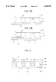
- FIG. 27A is an enlarged sectional view showing a part of a test board 10W according to the twenty-fourth embodiment.
- FIG. 27B is an enlarged bottom view of a part of the test board 10W.
- the test board 10W features formation of a slit 35 on that part of a conductive part 12B which is in contact with the projection electrode 17 so that the conductive part 12B is deformable around the slit 35.
- the slit 35 may be cross-shaped or has other configurations. The deformability of the conductive part 12B is controlled depending on the configuration of the slit 35 and the elasticity of the conductive part 12B.
- the conductive part 12B is deformed by the pressure from the projection electrode 17 when the semiconductor device 16 is mounted on the test board 10W. Since the conductive part 12B is deformed, the connect pressure exerted on the projection electrode 17 is canceled and the area of contact between the conductive part 12B and the projection electrode 17 is increased. Accordingly, the dual objectives of preventing deformation of the projection electrode 17 and improving electrical connection between the projection electrode 17 and the conductive part 12B are achieved.
Abstract
Description
Claims (33)
Priority Applications (1)
| Application Number | Priority Date | Filing Date | Title |
|---|---|---|---|
| US08/852,159 US6046598A (en) | 1994-11-18 | 1997-05-06 | Test board and a test method using the same providing improved electrical connection |
Applications Claiming Priority (5)
| Application Number | Priority Date | Filing Date | Title |
|---|---|---|---|
| JP28534294 | 1994-11-18 | ||
| US08/531,449 US5854558A (en) | 1994-11-18 | 1995-09-21 | Test board for testing a semiconductor device and method of testing the semiconductor device |
| JP9-019214 | 1997-01-31 | ||
| JP01921497A JP3233867B2 (en) | 1997-01-31 | 1997-01-31 | Test substrate and test method using the same |
| US08/852,159 US6046598A (en) | 1994-11-18 | 1997-05-06 | Test board and a test method using the same providing improved electrical connection |
Publications (1)
| Publication Number | Publication Date |
|---|---|
| US6046598A true US6046598A (en) | 2000-04-04 |
Family
ID=29424196
Family Applications (1)
| Application Number | Title | Priority Date | Filing Date |
|---|---|---|---|
| US08/852,159 Expired - Lifetime US6046598A (en) | 1994-11-18 | 1997-05-06 | Test board and a test method using the same providing improved electrical connection |
Country Status (1)
| Country | Link |
|---|---|
| US (1) | US6046598A (en) |
Cited By (12)
| Publication number | Priority date | Publication date | Assignee | Title |
|---|---|---|---|---|
| US6232791B1 (en) * | 1998-10-27 | 2001-05-15 | Matsushita Electric Industrial Co., Ltd. | Testing Board |
| US6316952B1 (en) * | 1999-05-12 | 2001-11-13 | Micron Technology, Inc. | Flexible conductive structures and method |
| US6388461B2 (en) * | 1997-03-19 | 2002-05-14 | Fujitsu Limited | Semiconductor inspection apparatus and inspection method using the apparatus |
| US6404214B1 (en) * | 1998-12-21 | 2002-06-11 | Shinko Electric Industries Co., Ltd. | Substrate for inspecting electronic device, method of manufacturing substrate, and method of inspecting electronic device |
| US6407563B2 (en) * | 1999-03-12 | 2002-06-18 | Oki Electric Industry Co, Ltd. | Semiconductor device test apparatus |
| US6448647B1 (en) | 1997-06-05 | 2002-09-10 | Sony Chemicals Corporation | BGA package substrate |
| US6466046B1 (en) * | 1998-12-18 | 2002-10-15 | Fujitsu Limited | Contactor for semiconductor devices, a testing apparatus using such contactor, a testing method using such contactor, and a method of cleaning such contactor |
| US6498503B2 (en) * | 1996-04-01 | 2002-12-24 | Micron Technology, Inc. | Semiconductor test interconnect with variable flexure contacts |
| US6597192B2 (en) * | 1999-01-29 | 2003-07-22 | Nitto Denko Corporation | Test method of semiconductor device |
| US20050023681A1 (en) * | 2000-12-11 | 2005-02-03 | Matsushita Electric Industrial Co., Ltd. | Viscous fluid transfer apparatus and transfer method, electronic component mounting apparatus and mounting method, and semiconductor device |
| CN102866318A (en) * | 2012-09-26 | 2013-01-09 | 贵州航天计量测试技术研究所 | Test device for laminar packaging discrete device |
| CN105044391A (en) * | 2014-04-24 | 2015-11-11 | 日本电产理德股份有限公司 | Electrode structure inspection jig and method of manufacturing electrode structure |
Citations (6)
| Publication number | Priority date | Publication date | Assignee | Title |
|---|---|---|---|---|
| JPS59208469A (en) * | 1983-05-13 | 1984-11-26 | Hitachi Micro Comput Eng Ltd | Probe card |
| JPS6377129A (en) * | 1986-09-19 | 1988-04-07 | Oki Electric Ind Co Ltd | Probe card |
| JPH05283490A (en) * | 1992-04-02 | 1993-10-29 | Fuji Electric Co Ltd | Testing method for integrated circuit device |
| JPH0735771A (en) * | 1993-07-23 | 1995-02-07 | Hitachi Ltd | Inspecting jig for electric characteristic of semiconductor device |
| US5500605A (en) * | 1993-09-17 | 1996-03-19 | At&T Corp. | Electrical test apparatus and method |
| US5519331A (en) * | 1994-11-10 | 1996-05-21 | Lsi Logic Corporation | Removable biasing board for automated testing of integrated circuits |
-
1997
- 1997-05-06 US US08/852,159 patent/US6046598A/en not_active Expired - Lifetime
Patent Citations (6)
| Publication number | Priority date | Publication date | Assignee | Title |
|---|---|---|---|---|
| JPS59208469A (en) * | 1983-05-13 | 1984-11-26 | Hitachi Micro Comput Eng Ltd | Probe card |
| JPS6377129A (en) * | 1986-09-19 | 1988-04-07 | Oki Electric Ind Co Ltd | Probe card |
| JPH05283490A (en) * | 1992-04-02 | 1993-10-29 | Fuji Electric Co Ltd | Testing method for integrated circuit device |
| JPH0735771A (en) * | 1993-07-23 | 1995-02-07 | Hitachi Ltd | Inspecting jig for electric characteristic of semiconductor device |
| US5500605A (en) * | 1993-09-17 | 1996-03-19 | At&T Corp. | Electrical test apparatus and method |
| US5519331A (en) * | 1994-11-10 | 1996-05-21 | Lsi Logic Corporation | Removable biasing board for automated testing of integrated circuits |
Cited By (27)
| Publication number | Priority date | Publication date | Assignee | Title |
|---|---|---|---|---|
| US6982564B2 (en) | 1996-04-01 | 2006-01-03 | Micron Technology, Inc. | Semiconductor test interconnect with variable flexure contacts |
| US7259578B2 (en) | 1996-04-01 | 2007-08-21 | Micron Technology, Inc. | System for testing semiconductor components having interconnect with variable flexure contacts |
| US7129725B2 (en) | 1996-04-01 | 2006-10-31 | Micron Technology, Inc. | Semiconductor test interconnect with variable flexure contacts having polymer material |
| US20060181294A1 (en) * | 1996-04-01 | 2006-08-17 | Salman Akram | System for testing semiconductor components having interconnect with variable flexure contacts |
| US6498503B2 (en) * | 1996-04-01 | 2002-12-24 | Micron Technology, Inc. | Semiconductor test interconnect with variable flexure contacts |
| US20030090282A1 (en) * | 1996-04-01 | 2003-05-15 | Salman Akram | Semiconductor test interconnect with variable flexure contacts |
| US20060001439A1 (en) * | 1996-04-01 | 2006-01-05 | Salman Akram | Semiconductor test interconnect with variable flexure contacts having polymer material |
| US6388461B2 (en) * | 1997-03-19 | 2002-05-14 | Fujitsu Limited | Semiconductor inspection apparatus and inspection method using the apparatus |
| US6448647B1 (en) | 1997-06-05 | 2002-09-10 | Sony Chemicals Corporation | BGA package substrate |
| US6232791B1 (en) * | 1998-10-27 | 2001-05-15 | Matsushita Electric Industrial Co., Ltd. | Testing Board |
| US6466046B1 (en) * | 1998-12-18 | 2002-10-15 | Fujitsu Limited | Contactor for semiconductor devices, a testing apparatus using such contactor, a testing method using such contactor, and a method of cleaning such contactor |
| US6781395B2 (en) | 1998-12-18 | 2004-08-24 | Fujitsu Limited | Contactor for semiconductor devices, a testing apparatus using such contactor, a testing method using such contactor, and a method of cleaning such contactor |
| US6603325B2 (en) | 1998-12-18 | 2003-08-05 | Fujitsu Limited | Contactor for semiconductor devices, a testing apparatus using such contactor, a testing method using such contactor, and a method of cleaning such contactor |
| US20030197501A1 (en) * | 1998-12-18 | 2003-10-23 | Fujitsu Limited | Contactor for semiconductor devices, a testing apparatus using such contactor, a testing method using such contactor, and a method of cleaning such contactor |
| US6404214B1 (en) * | 1998-12-21 | 2002-06-11 | Shinko Electric Industries Co., Ltd. | Substrate for inspecting electronic device, method of manufacturing substrate, and method of inspecting electronic device |
| US6597192B2 (en) * | 1999-01-29 | 2003-07-22 | Nitto Denko Corporation | Test method of semiconductor device |
| US7262610B2 (en) * | 1999-03-12 | 2007-08-28 | Oki Electric Industry Co., Ltd. | Method for manufacturing and testing semiconductor devices on a resin-coated wafer |
| US7639027B2 (en) | 1999-03-12 | 2009-12-29 | Oki Semiconductor Co., Ltd. | Method of testing circuit elements on a semiconductor wafer |
| US6879169B2 (en) * | 1999-03-12 | 2005-04-12 | Oki Electric Industry Co., Ltd. | Method for manufacturing and batch testing semiconductor devices |
| US6407563B2 (en) * | 1999-03-12 | 2002-06-18 | Oki Electric Industry Co, Ltd. | Semiconductor device test apparatus |
| US20070194802A1 (en) * | 1999-03-12 | 2007-08-23 | Oki Electric Industry Co., Ltd. | Method of testing circuit elements on a semiconductor wafer |
| US6316952B1 (en) * | 1999-05-12 | 2001-11-13 | Micron Technology, Inc. | Flexible conductive structures and method |
| US20050023681A1 (en) * | 2000-12-11 | 2005-02-03 | Matsushita Electric Industrial Co., Ltd. | Viscous fluid transfer apparatus and transfer method, electronic component mounting apparatus and mounting method, and semiconductor device |
| CN102866318A (en) * | 2012-09-26 | 2013-01-09 | 贵州航天计量测试技术研究所 | Test device for laminar packaging discrete device |
| CN102866318B (en) * | 2012-09-26 | 2015-07-22 | 贵州航天计量测试技术研究所 | Test device for laminar packaging discrete device |
| CN105044391A (en) * | 2014-04-24 | 2015-11-11 | 日本电产理德股份有限公司 | Electrode structure inspection jig and method of manufacturing electrode structure |
| CN105044391B (en) * | 2014-04-24 | 2019-10-25 | 日本电产理德股份有限公司 | Electrode assembly detects the manufacturing method of fixture and electrode assembly |
Similar Documents
| Publication | Publication Date | Title |
|---|---|---|
| US6075710A (en) | Low-cost surface-mount compatible land-grid array (LGA) chip scale package (CSP) for packaging solder-bumped flip chips | |
| US5726502A (en) | Bumped semiconductor device with alignment features and method for making the same | |
| US5534784A (en) | Method for probing a semiconductor wafer | |
| KR101227228B1 (en) | Wire bond interconnection | |
| US7176043B2 (en) | Microelectronic packages and methods therefor | |
| US8759973B2 (en) | Microelectronic assemblies having compliancy and methods therefor | |
| US6826827B1 (en) | Forming conductive posts by selective removal of conductive material | |
| US5880590A (en) | Apparatus and method for burn-in and testing of devices with solder bumps or preforms | |
| KR100430208B1 (en) | Test assembly | |
| US7719121B2 (en) | Microelectronic packages and methods therefor | |
| US6836011B2 (en) | Semiconductor chip mounting structure with movable connection electrodes | |
| US6177636B1 (en) | Connection components with posts | |
| US6939143B2 (en) | Flexible compliant interconnect assembly | |
| JP4150695B2 (en) | Contact carrier (tile) for placing spring contacts on larger substrates | |
| US6046598A (en) | Test board and a test method using the same providing improved electrical connection | |
| US6861858B2 (en) | Vertical probe card and method for using the same | |
| US20030110626A1 (en) | Method of locating conductive spheres utilizing screen and hopper of solder balls | |
| US20060125501A1 (en) | Modularized probe head | |
| US5854558A (en) | Test board for testing a semiconductor device and method of testing the semiconductor device | |
| KR20050106581A (en) | Structure of flip chip semiconductor package for testing a bump and method of fabricating the same | |
| US20060033515A1 (en) | Test fixture with movable pin contacts | |
| US6428908B1 (en) | Contact and method for producing a contact | |
| JPH08220140A (en) | Probe card and manufacture thereof | |
| US7028398B2 (en) | Contactor, a method of manufacturing the contactor and a device and method of testing electronic component using the contactor | |
| JP3233867B2 (en) | Test substrate and test method using the same |
Legal Events
| Date | Code | Title | Description |
|---|---|---|---|
| AS | Assignment |
Owner name: FUJITSU LIMITED, JAPAN Free format text: ASSIGNMENT OF ASSIGNORS INTEREST;ASSIGNORS:MIYAJI, NAOMI;MORIYA, SUSUMU;MARUYAMA, SHIGEYUKI;AND OTHERS;REEL/FRAME:008544/0001 Effective date: 19970424 |
|
| AS | Assignment |
Owner name: FUJITSU LIMITED, JAPAN Free format text: ASSIGNMENT OF ASSIGNOR'S INTEREST (RE-RECORD TO CORRECT THE RECORDATION DATE 5/2/97 RECORDED ON REEL 8544, FRAME 0001);ASSIGNORS:MIYAJI, NAOMI;MORIYA, SUSUMU;MARUYAMA, SHIGEYUKI;AND OTHERS;REEL/FRAME:008735/0047 Effective date: 19970424 |
|
| STCF | Information on status: patent grant |
Free format text: PATENTED CASE |
|
| FEPP | Fee payment procedure |
Free format text: PAYOR NUMBER ASSIGNED (ORIGINAL EVENT CODE: ASPN); ENTITY STATUS OF PATENT OWNER: LARGE ENTITY |
|
| FPAY | Fee payment |
Year of fee payment: 4 |
|
| CC | Certificate of correction | ||
| FPAY | Fee payment |
Year of fee payment: 8 |
|
| AS | Assignment |
Owner name: FUJITSU MICROELECTRONICS LIMITED, JAPAN Free format text: ASSIGNMENT OF ASSIGNORS INTEREST;ASSIGNOR:FUJITSU LIMITED;REEL/FRAME:021976/0876 Effective date: 20081104 Owner name: FUJITSU MICROELECTRONICS LIMITED,JAPAN Free format text: ASSIGNMENT OF ASSIGNORS INTEREST;ASSIGNOR:FUJITSU LIMITED;REEL/FRAME:021976/0876 Effective date: 20081104 |
|
| AS | Assignment |
Owner name: FUJITSU SEMICONDUCTOR LIMITED, JAPAN Free format text: CHANGE OF NAME;ASSIGNOR:FUJITSU MICROELECTRONICS LIMITED;REEL/FRAME:024804/0269 Effective date: 20100401 |
|
| FPAY | Fee payment |
Year of fee payment: 12 |
|
| AS | Assignment |
Owner name: SOCIONEXT INC., JAPAN Free format text: ASSIGNMENT OF ASSIGNORS INTEREST;ASSIGNOR:FUJITSU SEMICONDUCTOR LIMITED;REEL/FRAME:035508/0637 Effective date: 20150302 |