US6067132A - LCD having contact electrode coupling gate electrode of first pixel to region active layer of second pixel region - Google Patents
LCD having contact electrode coupling gate electrode of first pixel to region active layer of second pixel region Download PDFInfo
- Publication number
- US6067132A US6067132A US08/917,382 US91738297A US6067132A US 6067132 A US6067132 A US 6067132A US 91738297 A US91738297 A US 91738297A US 6067132 A US6067132 A US 6067132A
- Authority
- US
- United States
- Prior art keywords
- region
- active layer
- gate
- electrode
- contact
- Prior art date
- Legal status (The legal status is an assumption and is not a legal conclusion. Google has not performed a legal analysis and makes no representation as to the accuracy of the status listed.)
- Expired - Lifetime
Links
Images


Classifications
-
- G—PHYSICS
- G02—OPTICS
- G02F—OPTICAL DEVICES OR ARRANGEMENTS FOR THE CONTROL OF LIGHT BY MODIFICATION OF THE OPTICAL PROPERTIES OF THE MEDIA OF THE ELEMENTS INVOLVED THEREIN; NON-LINEAR OPTICS; FREQUENCY-CHANGING OF LIGHT; OPTICAL LOGIC ELEMENTS; OPTICAL ANALOGUE/DIGITAL CONVERTERS
- G02F1/00—Devices or arrangements for the control of the intensity, colour, phase, polarisation or direction of light arriving from an independent light source, e.g. switching, gating or modulating; Non-linear optics
- G02F1/01—Devices or arrangements for the control of the intensity, colour, phase, polarisation or direction of light arriving from an independent light source, e.g. switching, gating or modulating; Non-linear optics for the control of the intensity, phase, polarisation or colour
- G02F1/13—Devices or arrangements for the control of the intensity, colour, phase, polarisation or direction of light arriving from an independent light source, e.g. switching, gating or modulating; Non-linear optics for the control of the intensity, phase, polarisation or colour based on liquid crystals, e.g. single liquid crystal display cells
- G02F1/133—Constructional arrangements; Operation of liquid crystal cells; Circuit arrangements
- G02F1/136—Liquid crystal cells structurally associated with a semi-conducting layer or substrate, e.g. cells forming part of an integrated circuit
- G02F1/1362—Active matrix addressed cells
- G02F1/136213—Storage capacitors associated with the pixel electrode
-
- G—PHYSICS
- G02—OPTICS
- G02F—OPTICAL DEVICES OR ARRANGEMENTS FOR THE CONTROL OF LIGHT BY MODIFICATION OF THE OPTICAL PROPERTIES OF THE MEDIA OF THE ELEMENTS INVOLVED THEREIN; NON-LINEAR OPTICS; FREQUENCY-CHANGING OF LIGHT; OPTICAL LOGIC ELEMENTS; OPTICAL ANALOGUE/DIGITAL CONVERTERS
- G02F1/00—Devices or arrangements for the control of the intensity, colour, phase, polarisation or direction of light arriving from an independent light source, e.g. switching, gating or modulating; Non-linear optics
- G02F1/01—Devices or arrangements for the control of the intensity, colour, phase, polarisation or direction of light arriving from an independent light source, e.g. switching, gating or modulating; Non-linear optics for the control of the intensity, phase, polarisation or colour
- G02F1/13—Devices or arrangements for the control of the intensity, colour, phase, polarisation or direction of light arriving from an independent light source, e.g. switching, gating or modulating; Non-linear optics for the control of the intensity, phase, polarisation or colour based on liquid crystals, e.g. single liquid crystal display cells
- G02F1/133—Constructional arrangements; Operation of liquid crystal cells; Circuit arrangements
- G02F1/1333—Constructional arrangements; Manufacturing methods
- G02F1/1343—Electrodes
-
- G—PHYSICS
- G02—OPTICS
- G02F—OPTICAL DEVICES OR ARRANGEMENTS FOR THE CONTROL OF LIGHT BY MODIFICATION OF THE OPTICAL PROPERTIES OF THE MEDIA OF THE ELEMENTS INVOLVED THEREIN; NON-LINEAR OPTICS; FREQUENCY-CHANGING OF LIGHT; OPTICAL LOGIC ELEMENTS; OPTICAL ANALOGUE/DIGITAL CONVERTERS
- G02F1/00—Devices or arrangements for the control of the intensity, colour, phase, polarisation or direction of light arriving from an independent light source, e.g. switching, gating or modulating; Non-linear optics
- G02F1/01—Devices or arrangements for the control of the intensity, colour, phase, polarisation or direction of light arriving from an independent light source, e.g. switching, gating or modulating; Non-linear optics for the control of the intensity, phase, polarisation or colour
- G02F1/13—Devices or arrangements for the control of the intensity, colour, phase, polarisation or direction of light arriving from an independent light source, e.g. switching, gating or modulating; Non-linear optics for the control of the intensity, phase, polarisation or colour based on liquid crystals, e.g. single liquid crystal display cells
- G02F1/133—Constructional arrangements; Operation of liquid crystal cells; Circuit arrangements
- G02F1/136—Liquid crystal cells structurally associated with a semi-conducting layer or substrate, e.g. cells forming part of an integrated circuit
- G02F1/1362—Active matrix addressed cells
- G02F1/1368—Active matrix addressed cells in which the switching element is a three-electrode device
-
- H—ELECTRICITY
- H01—ELECTRIC ELEMENTS
- H01L—SEMICONDUCTOR DEVICES NOT COVERED BY CLASS H10
- H01L27/00—Devices consisting of a plurality of semiconductor or other solid-state components formed in or on a common substrate
- H01L27/02—Devices consisting of a plurality of semiconductor or other solid-state components formed in or on a common substrate including semiconductor components specially adapted for rectifying, oscillating, amplifying or switching and having at least one potential-jump barrier or surface barrier; including integrated passive circuit elements with at least one potential-jump barrier or surface barrier
- H01L27/12—Devices consisting of a plurality of semiconductor or other solid-state components formed in or on a common substrate including semiconductor components specially adapted for rectifying, oscillating, amplifying or switching and having at least one potential-jump barrier or surface barrier; including integrated passive circuit elements with at least one potential-jump barrier or surface barrier the substrate being other than a semiconductor body, e.g. an insulating body
- H01L27/1214—Devices consisting of a plurality of semiconductor or other solid-state components formed in or on a common substrate including semiconductor components specially adapted for rectifying, oscillating, amplifying or switching and having at least one potential-jump barrier or surface barrier; including integrated passive circuit elements with at least one potential-jump barrier or surface barrier the substrate being other than a semiconductor body, e.g. an insulating body comprising a plurality of TFTs formed on a non-semiconducting substrate, e.g. driving circuits for AMLCDs
- H01L27/124—Devices consisting of a plurality of semiconductor or other solid-state components formed in or on a common substrate including semiconductor components specially adapted for rectifying, oscillating, amplifying or switching and having at least one potential-jump barrier or surface barrier; including integrated passive circuit elements with at least one potential-jump barrier or surface barrier the substrate being other than a semiconductor body, e.g. an insulating body comprising a plurality of TFTs formed on a non-semiconducting substrate, e.g. driving circuits for AMLCDs with a particular composition, shape or layout of the wiring layers specially adapted to the circuit arrangement, e.g. scanning lines in LCD pixel circuits
-
- H—ELECTRICITY
- H01—ELECTRIC ELEMENTS
- H01L—SEMICONDUCTOR DEVICES NOT COVERED BY CLASS H10
- H01L27/00—Devices consisting of a plurality of semiconductor or other solid-state components formed in or on a common substrate
- H01L27/02—Devices consisting of a plurality of semiconductor or other solid-state components formed in or on a common substrate including semiconductor components specially adapted for rectifying, oscillating, amplifying or switching and having at least one potential-jump barrier or surface barrier; including integrated passive circuit elements with at least one potential-jump barrier or surface barrier
- H01L27/12—Devices consisting of a plurality of semiconductor or other solid-state components formed in or on a common substrate including semiconductor components specially adapted for rectifying, oscillating, amplifying or switching and having at least one potential-jump barrier or surface barrier; including integrated passive circuit elements with at least one potential-jump barrier or surface barrier the substrate being other than a semiconductor body, e.g. an insulating body
- H01L27/1214—Devices consisting of a plurality of semiconductor or other solid-state components formed in or on a common substrate including semiconductor components specially adapted for rectifying, oscillating, amplifying or switching and having at least one potential-jump barrier or surface barrier; including integrated passive circuit elements with at least one potential-jump barrier or surface barrier the substrate being other than a semiconductor body, e.g. an insulating body comprising a plurality of TFTs formed on a non-semiconducting substrate, e.g. driving circuits for AMLCDs
- H01L27/1255—Devices consisting of a plurality of semiconductor or other solid-state components formed in or on a common substrate including semiconductor components specially adapted for rectifying, oscillating, amplifying or switching and having at least one potential-jump barrier or surface barrier; including integrated passive circuit elements with at least one potential-jump barrier or surface barrier the substrate being other than a semiconductor body, e.g. an insulating body comprising a plurality of TFTs formed on a non-semiconducting substrate, e.g. driving circuits for AMLCDs integrated with passive devices, e.g. auxiliary capacitors
Definitions
- the present invention relates to a liquid crystal display device, and more particularly to a liquid crystal display device and a method of fabricating the same.
- a liquid crystal display device includes two glass plates, i.e., a bottom plate and a top plate, in which a liquid crystal is injected therebetween.
- a thin film transistor and a pixel electrode are arranged on the bottom plate.
- the top plate has a color filter layer for displaying a color, a common electrode, and a black matrix layer.
- FIG. 1 is a circuit diagram of a conventional liquid crystal display device. Referring to FIG. 1, a plurality of gate lines are disposed in one direction at a predetermined interval and a plurality of data lines are disposed perpendicular to the gate lines at a predetermined interval.
- a plurality of thin film transistors are formed between the respective gate line and the respective data line in a matrix arrangement so as to apply signals of the data lines as well as the gate lines to the pixel electrode.
- a stacked storage capacitor and a liquid crystal capacitor having a liquid crystal layer as a dielectric are formed in the pixel electrode.
- FIG. 2 is a layout illustrating a bottom plate of a conventional liquid crystal display device.
- FIGS. 3A-3H are sectional views illustrating fabricating process steps of a liquid crystal display device taken along I--I line of FIG. 2.
- polysilicon is formed on a transparent insulating substrate 1 of glass or quartz and patterned to form an island shaped active layer 2.
- the active layer 2 serves as an active region of the thin film transistor and an electrode of the storage capacitor.
- a photoresist 3 is coated on an entire surface of the substrate 1 and patterned to expose the active layer 2 which will be a lower electrode of the storage capacitor. Impurity ions such as phosphorus P or boron B are implanted into the exposed active layer 2 using the photoresist 3 as a mask.
- the photoresist 3 is removed and a gate insulating film 4 is formed on the entire surface of the substrate 1 including the active layer 2.
- Polysilicon containing impurity ions is deposited on the entire surface of the substrate 1 including the gate insulating film 4.
- Silicide material such as WSix or MoSix is then deposited thereon and patterned to define gate electrodes 5 and 5' and upper electrodes 5a and 5a' of the storage capacitor.
- the gate electrodes 5 and 5' are used as the gate line and the upper electrodes 5a and 5a' are used as the common electrode.
- the impurity ions such as phosphorus or boron are implanted into the active layer 2 using the gate electrodes 5 and 5' as masks and the impurity ions are activated by heat treatment to define source and drain regions of the thin film transistor.
- a first interlayer insulating film 6 is deposited on the entire surface of the substrate 1 including the gate electrodes 5 and 5'.
- a first contact hole 7 is formed by selectively removing the gate insulating film 4 and the first interlayer insulating film 6 to expose the source region of the active layer 2.
- a metal is deposited on the entire surface of the substrate 1 including the first interlayer insulating film 6 and patterned so that a data line 8 is formed to be connected with the active layer 2 through the first contact hole 7.
- a second interlayer insulating film 9 is deposited on the entire surface of the substrate 1 including the data line 8.
- a second contact hole 10 is formed by selectively removing the gate insulating film 4 and the first and second interlayer insulating films 6 and 9 to expose the drain region of the active layer 2.
- a transparent conductive material such as Indium Tin Oxide (ITO) is deposited on the second interlayer insulating film 9 and patterned.
- a pixel electrode 11 is then formed to be connected with the active layer 2 through the second contact hole 10.
- the active layer 2 is hydrogenated to remove its defects.
- ITO Indium Tin Oxide
- a protective film 12 is formed on the entire surface of the substrate 1 including the pixel electrode 11 and a pad is open. As a result, the lower plate of the liquid crystal display device is completed.
- the conventional liquid crystal display device has several problems.
- the storage capacitor has an opaque stacked structure of the active layer, the gate insulating film, and the gate electrode, aperture ratio is reduced as much as an area 15-25% of the pixel region due to the storage capacitor.
- the suicide material such as WSix or MoSix is deposited on the polysilicon containing the impurity ions to be used as the gate electrode material, there are problems in that the step of forming the suicide material is complicated and resistance becomes larger than that of the metal material.
- the photoresist is patterned on the active layer and the impurity ions are implanted into the active layer to define the lower electrode region of the storage capacitor.
- the step of removing the photoresist is difficult and the surface of the active layer is damaged during that step of removing the photoresist, thereby deteriorating characteristics of the device.
- the present invention is directed to a liquid crystal display device and a method for fabricating the same that substantially obviates one or more of the above problems, limitations and disadvantages of the related art.
- An object of the present invention is to provide a liquid crystal display device and a method for fabricating the same, which improves aperture ratio.
- a liquid crystal display device having a plurality of matrix shaped pixel regions, and a plurality of gate lines and data lines perpendicular to each other between the pixel regions, includes a first active layer having source and drain regions in a first region on a substrate, a second active layer in a second region on the substrate, a gate electrode formed between the source region and drain regions of the first active layer in contact with the gate lines, a first pixel electrode formed in the pixel regions in contact with the drain region of the first active layer, and a contact electrode formed to be connected with the gate electrode in contact with the second active layer.
- a method for fabricating a liquid crystal display device having a thin film transistor and a storage capacitor, includes the steps of forming a first active layer in a thin film transistor region on a substrate, forming a second active layer in a storage capacitor region, forming a first insulating film on the first and second active layers, forming a gate electrode in the thin film transistor region, implanting impurity ions into the first active layer using the gate electrode as a mask to form source and drain regions of the thin film transistor, forming a first pixel electrode to be connected with the drain region of the first active layer, forming a contact electrode to be connected with the second active layer and the gate electrode, forming a second insulating film on an entire surface of the substrate including the first and pixel electrode the contact electrode, forming data lines to be connected with the source region of the first active layer, forming a third insulating film on the entire surface including the data lines, forming gate lines to be connected with the gate electrode, and forming a protective film on
- a liquid crystal display device having a plurality of matrix shaped pixel regions, and a plurality of gate lines and data lines perpendicular to each other between the pixel regions, includes a first active layer having source and drain regions in a first region on a substrate, a second active layer in a second region on the substrate, a gate electrode formed between the source and drain regions of the first active layer in contact with gate lines, a first pixel electrode formed in the pixel regions in contact with the drain region of the first active layer, and a contact electrode formed in a data line region in contact with the second active layer.
- a method for fabricating a liquid crystal display device having a thin film transistor and a storage capacitor, includes the steps of forming a first active layer in a thin film transistor region on a substrate, forming a second active layer in a storage capacitor region, forming a first insulating film on the first and second active layers, forming a gate electrode in the thin film transistor region, implanting impurity ions into the first active layer using the gate electrode as a mask to form source and drain regions of the thin film transistor, forming a first pixel electrode to be connected with the drain region of the first active layer, forming a contact electrode to be connected with a predetermined region of the second active layer, forming a second insulating film on an entire surface of the substrate including the first pixel electrode and the contact electrode electrodes, forming data lines in an integral form with the contact electrode to be connected with the source region of the first active layer, forming a third insulating film on the entire surface of the substrate including the data lines, forming gate lines
- FIG. 1 is a circuit diagram illustrating a conventional liquid crystal display device
- FIG. 2 is a layout illustrating a conventional liquid crystal display device
- FIGS. 3A-3H are sectional views illustrating fabricating process steps of a liquid crystal display device taken along I--I line of FIG. 2;
- FIG. 4A is a circuit diagram illustrating a liquid crystal display device according to a first embodiment of the present invention.
- FIG. 4B is a layout illustrating a liquid crystal display device according to the first embodiment of the present invention.
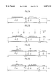
- FIGS. 5A-5G are sectional views illustrating fabricating process steps of a liquid crystal display device taken along II--II line and III--III line of FIG. 4B;
- FIG. 6 is a layout illustrating a liquid crystal display device according to a second embodiment of the present invention.
- FIGS. 7A-7H are sectional views illustrating fabricating process steps of a liquid crystal display device taken along IV--IV line, V--V line, and VI--VI line of FIG. 6.
- a plurality of gate lines 41 are formed at a predetermined interval and a plurality of data lines 38 are formed in a direction perpendicular to the gate lines 41 at a predetermined interval.
- an island shaped first active layer 31 having source and drain regions is formed in a thin film transistor region on a substrate in which the gate lines 41 and the data lines 38 are formed.
- an island shaped second active layer 31' is formed in a storage capacitor region.
- a gate electrode 33 is formed between the source and drain regions of the first active layer 31 in contact with the gate line 41. At this time, the gate electrode 33 and the gate line 41 are made of different material from each other.
- a first pixel electrode 35 is formed in contact with the drain region of the first active layer 31.
- a contact electrode 35' is formed in contact with the second active layer 31' to be connected with the gate electrode 33.
- the pixel electrode 35' is disposed below the gate line 41.
- the gate electrode 33 and the second active layer 31' in which the storage capacitor will be formed are connected to each other by the contact electrode 35'.
- the first active layer 31 and the second active layer 31' are respectively formed in the thin film transistor region and the pixel region on a transparent insulating substrate 30 of glass or quartz and then patterned in island shapes.
- a gate insulating film 32 is formed on the entire surface on the first and second active layers 31 and 31'.
- the first gate electrode material is deposited on the entire surface of the substrate 30 including the gate insulating film 32 and patterned to form the gate electrode 33.
- a polysilicon containing impurity ions such as boron or phosphorus is used as the first gate electrode material to facilitate the hydrogenation process in which hydrogen radicals are diffused into the active layer to improve performance of the thin film transistor.
- the source and drain regions are defined by implanting the impurity ions such as phosphorus or boron into the first active layer 31 using the gate electrode 33 as a mask. At this time, the impurity ions are naturally implanted into the second active layer 31' in which the storage capacitor will be formed, so that the lower electrode of the storage capacitor is defined.
- the impurity ions implanted into the first and second active layers 31 and 31' are activated by heat treatment.
- the gate insulating film 32 on the drain region of the first active layer 31 and on the second active layer 31' in which the storage capacitor will be formed is partially removed to form first and second contact holes 34 and 34', respectively.
- a transparent conductive material such as ITO is coated on the second active layer 31' and patterned.
- the first pixel electrode 35 is then formed to be connected with the drain region of the first active layer 31 through the first contact hole 34.
- the contact electrode 35' is formed to be connected with the second active layer 31', in which the storage capacitor will be formed, through the second contact hole 34' and at the same time to be connected with the gate electrode 33.
- a first interlayer insulating film 36 is deposited on the entire surface of the substrate 30 including the first pixel electrode 35 and the contact electrode 35'.
- a third contact hole 37 is formed by selectively removing the gate insulating film 32 and the first interlayer insulating film 36 to expose the source region of the first active layer 31.
- a metal is deposited on the entire surface of the substrate 30 including the first interlayer insulating film 36 and patterned.
- the data line 38 is then formed to be connected with the first active layer 31 through the third contact hole 37.
- a second interlayer insulating film 39 is deposited on the entire surface of the substrate 30 including the data line 38.
- a fourth contact hole 40 is formed by selectively removing the first and second interlayer insulating films 36 and 39 to expose the gate electrode 33.
- the second gate electrode material is deposited on the entire surface of the substrate 30 including the second interlayer insulating film 39 and patterned.
- the gate line 41 is then formed to be connected with the gate electrode 33 through the fourth contact hole 40. At this time, metal material having very low resistance is used as the gate line 41.
- a protective film 42 is formed on the entire surface of the substrate 30 including the gate line 41.
- a liquid crystal display device according to a second embodiment of the present invention will now be described.
- a plurality of gate lines 71 are formed at a predetermined interval, and a plurality of data lines 68 are formed in a direction perpendicular to the gate lines 71 at a predetermined interval.
- An island shaped first active layer 61 having source and drain regions is formed in a thin film transistor region on a substrate in which the gate lines 71 and the data lines 68 are formed.
- An island shaped second active layer 61' is formed in a storage capacitor region on the substrate.
- a gate electrode 63 is formed between the source and drain regions of the first active layer 61 in contact with the gate line 71. At this time, the gate electrode 63 and the gate line 71 are made of different material from each other.
- a first pixel electrode 65 is formed in a pixel region in contact with the drain region of the first active layer 61.
- a contact electrode 65' is formed in a data region in an integral form in contact with the second active layer 61'.
- the first active layer 61 is formed in the thin film transistor region on a transparent insulating substrate 60 of glass or quartz and then patterned in an island shape.
- the second active layer 61' is formed in a region, in which the storage capacitor will be formed, and patterned in an island shape.
- the gate insulating film 62 is formed on the entire surface on the first and second active layers 61 and 61'.
- the first gate electrode material is deposited on the entire surface of the substrate 60 including the gate insulating film 62 and patterned to form the gate electrode 63.
- polysilicon containing impurity ions such as boron or phosphorus is used as the first gate electrode material to facilitate hydrogenation process.
- the source and drain regions are defined by implanting impurity ions such as phosphorus or boron into the first active layer 61 using the gate electrode 63 as a mask. At this time, the impurity ions are naturally implanted into the second active layer 61' so that a lower electrode of the storage capacitor is defined.
- the gate insulating film 62 on the drain region of the first active layer 61 and on the second active layer 61' in which the storage capacitor will be formed is partially removed to form first and second contact holes 64 and 64', respectively.
- a transparent conductive material such as ITO is deposited and patterned.
- the first pixel electrode 65 is then formed to be connected with the drain region of the first active layer 61 through the first contact hole 64.
- the contact electrode 65' is formed to be connected with the second active layer 61', in which the storage capacitor will be formed, through the second contact hole 64'.
- a first interlayer insulating film 66 is deposited on the entire surface of the substrate 60 including the first pixel electrode 65 and the contact electrode 65'.
- a third contact hole 67 is formed by selectively removing the gate insulating film 62 and the first interlayer insulating film 66 to expose the source region of the first active layer 61.
- a metal is deposited on the entire surface of the substrate 60 including the first interlayer insulating film 66 and patterned.
- the data line 68 is then formed to be connected with the first active layer 61 through the third contact hole 67.
- a second interlayer insulating film 69 is deposited on the entire surface of the substrate 60 including the data line 68.
- a fourth contact hole 70 is formed by selectively removing the first and second interlayer insulating films 66 and 69 to expose the gate electrode 63.
- the second gate electrode material is deposited on the entire surface of the substrate 60 including the second interlayer insulating film 69 and patterned.
- the gate line 71 is then formed to be connected with the gate electrode 63 through the fourth contact hole 70.
- a metal material having very low resistance is used as the gate line 71.
- the first and second active layers 61 and 61' are hydrogenated to remove their defects and improve performance of the thin film transistor.
- a protective film 72 is formed on the entire surface of the substrate 60 including the gate line 71.
- the liquid crystal display device and the method for fabricating the same according to the present invention have the following advantages.
- the storage capacitor has a transparent structure formed of the active layer, the gate insulating film, and the pixel electrode, aperture is improved, thereby yielding a liquid crystal display device having high definition.
- the lower electrode of the storage capacitor is defined when the source and drain regions of the thin film transistor are defined.
Abstract
Description
Claims (20)
Applications Claiming Priority (2)
| Application Number | Priority Date | Filing Date | Title |
|---|---|---|---|
| KR1019960037539A KR100209620B1 (en) | 1996-08-31 | 1996-08-31 | Liquid crystal display device and its manufacturing method |
| KR96-37539 | 1996-08-31 |
Publications (1)
| Publication Number | Publication Date |
|---|---|
| US6067132A true US6067132A (en) | 2000-05-23 |
Family
ID=19472283
Family Applications (1)
| Application Number | Title | Priority Date | Filing Date |
|---|---|---|---|
| US08/917,382 Expired - Lifetime US6067132A (en) | 1996-08-31 | 1997-08-26 | LCD having contact electrode coupling gate electrode of first pixel to region active layer of second pixel region |
Country Status (3)
| Country | Link |
|---|---|
| US (1) | US6067132A (en) |
| JP (1) | JP3116221B2 (en) |
| KR (1) | KR100209620B1 (en) |
Cited By (22)
| Publication number | Priority date | Publication date | Assignee | Title |
|---|---|---|---|---|
| US20010028071A1 (en) * | 2000-02-11 | 2001-10-11 | Soon-Sung Yoo | Array substrate for use in LCD device and method of fabricating same |
| US6317173B1 (en) * | 1997-12-31 | 2001-11-13 | Samsung Electronics Co., Ltd. | Liquid crystal displays, manufacturing methods and a driving method thereof |
| US20020021380A1 (en) * | 2000-08-09 | 2002-02-21 | Hitachi, Ltd. | Active matrix display device |
| US6421101B1 (en) * | 1996-09-04 | 2002-07-16 | Semiconductor Energy Laboratory Co., Ltd. | Display device including a transparent electrode pattern covering and extending along gate & source lines |
| US6593592B1 (en) * | 1999-01-29 | 2003-07-15 | Semiconductor Energy Laboratory Co., Ltd. | Semiconductor device having thin film transistors |
| US20030201963A1 (en) * | 2002-04-30 | 2003-10-30 | International Business Machines Corporation | Liquid crystal display |
| EP1045451A3 (en) * | 1999-04-12 | 2006-08-02 | Semiconductor Energy Laboratory Co., Ltd. | Semiconductor device and method for fabricating the same |
| US20060226430A1 (en) * | 1999-03-19 | 2006-10-12 | Semiconductor Energy Laboratory Co., Ltd. | Electro-optical device and manufacturing method thereof |
| US7122835B1 (en) | 1999-04-07 | 2006-10-17 | Semiconductor Energy Laboratory Co., Ltd. | Electrooptical device and a method of manufacturing the same |
| US20060244889A1 (en) * | 2005-05-02 | 2006-11-02 | Ji-Won Sohn | Liquid crystal display and manufacturing method of the same |
| EP1087438A3 (en) * | 1999-09-27 | 2007-05-23 | Semiconductor Energy Laboratory Co., Ltd. | Semiconductor device and method of manufacturing therof |
| CN100429765C (en) * | 2006-12-04 | 2008-10-29 | 友达光电股份有限公司 | An array substrate of thin-film transistor and its manufacture method |
| US20090059109A1 (en) * | 2007-08-29 | 2009-03-05 | Min-Hyuk Choi | Array substrate and display panel having the same |
| US20090122241A1 (en) * | 2006-04-28 | 2009-05-14 | Hitoshi Satoh | Liquid crystal display device and manufacturing method of the same |
| US20090267073A1 (en) * | 2000-02-22 | 2009-10-29 | Semiconductor Energy Laboratory Co., Ltd. | Semiconductor Device and Method of Manufacturing the Same |
| US20100110320A1 (en) * | 2007-04-24 | 2010-05-06 | Hidehito Kitakado | Display device substrate, display device, and wiring substrate |
| US20110013106A1 (en) * | 2009-07-17 | 2011-01-20 | Beijing Boe Optoelectronics Technology Co., Ltd. | Tft-lcd array substrate and manufacturing method thereof |
| US20110090416A1 (en) * | 2009-10-21 | 2011-04-21 | Semiconductor Energy Laboratory Co., Ltd. | Liquid crystal display device and electronic device including the same |
| US20110210327A1 (en) * | 2010-02-26 | 2011-09-01 | Semiconductor Energy Laboratory Co., Ltd. | Liquid crystal display device |
| CN103094354A (en) * | 2013-01-28 | 2013-05-08 | 合肥京东方光电科技有限公司 | Array baseplate, manufacturing method and display device thereof |
| US8487315B2 (en) | 2000-04-12 | 2013-07-16 | Semiconductor Energy Laboratory Co., Ltd. | Illumination apparatus |
| US9608009B2 (en) | 2013-10-07 | 2017-03-28 | Lg Display Co., Ltd. | Display device and method of fabricating the same |
Families Citing this family (9)
| Publication number | Priority date | Publication date | Assignee | Title |
|---|---|---|---|---|
| JP3844913B2 (en) * | 1999-06-28 | 2006-11-15 | アルプス電気株式会社 | Active matrix type liquid crystal display device |
| JP5148032B2 (en) * | 2000-08-09 | 2013-02-20 | 株式会社ジャパンディスプレイイースト | Active matrix display device |
| KR20020091688A (en) * | 2001-05-31 | 2002-12-06 | 주식회사 현대 디스플레이 테크놀로지 | Tft lcd and method for manufacturing thereof |
| KR100433209B1 (en) | 2001-06-25 | 2004-05-27 | 엘지.필립스 엘시디 주식회사 | Array Substrate of Liquid Crystal Display Device and Fabricating Method Thereof |
| JP4305811B2 (en) * | 2001-10-15 | 2009-07-29 | 株式会社日立製作所 | Liquid crystal display device, image display device and manufacturing method thereof |
| KR100623232B1 (en) | 2003-11-29 | 2006-09-18 | 삼성에스디아이 주식회사 | flat panel display and fabrication method of the same |
| US7675582B2 (en) | 2004-12-03 | 2010-03-09 | Au Optronics Corporation | Stacked storage capacitor structure for a thin film transistor liquid crystal display |
| JP5766481B2 (en) * | 2011-03-29 | 2015-08-19 | 株式会社Joled | Display device and electronic device |
| KR102042484B1 (en) | 2017-03-31 | 2019-11-19 | 주식회사 선우씨앤에스 | form supporter of bracket for building upper layer installation |
Citations (7)
| Publication number | Priority date | Publication date | Assignee | Title |
|---|---|---|---|---|
| US5054887A (en) * | 1988-08-10 | 1991-10-08 | Sharp Kabushiki Kaisha | Active matrix type liquid crystal display |
| US5187602A (en) * | 1990-07-12 | 1993-02-16 | Kabushiki Kaisha Toshiba | Liquid crystal display apparatus |
| US5191451A (en) * | 1990-04-20 | 1993-03-02 | Sharp Kabushiki Kaisha | Active matrix display device having drain electrodes of the pair of tfts being symmetrically formed with respect to the central plane to prevent the flicker due to the different parasitic capacitances |
| US5212574A (en) * | 1989-07-05 | 1993-05-18 | Sharp Kabushiki Kaisha | Active matrix board having double-layer scan lines and capacity lines with discontinuous lower scan lines and lower capacity lines |
| US5737049A (en) * | 1995-05-09 | 1998-04-07 | Lg Electronics, Inc. | Liquid crystal display device having storage capacitors of increased capacitance and fabrication method therefor |
| US5745194A (en) * | 1994-06-28 | 1998-04-28 | Nec Corporation | Active matrix LCD apparatus with compensating capacitor having a particular feature |
| US5880794A (en) * | 1996-03-15 | 1999-03-09 | Lg Electronics, Inc. | Active matrix liquid crystal display and method with two anodizations |
-
1996
- 1996-08-31 KR KR1019960037539A patent/KR100209620B1/en not_active IP Right Cessation
-
1997
- 1997-08-26 US US08/917,382 patent/US6067132A/en not_active Expired - Lifetime
- 1997-08-27 JP JP09230798A patent/JP3116221B2/en not_active Expired - Fee Related
Patent Citations (7)
| Publication number | Priority date | Publication date | Assignee | Title |
|---|---|---|---|---|
| US5054887A (en) * | 1988-08-10 | 1991-10-08 | Sharp Kabushiki Kaisha | Active matrix type liquid crystal display |
| US5212574A (en) * | 1989-07-05 | 1993-05-18 | Sharp Kabushiki Kaisha | Active matrix board having double-layer scan lines and capacity lines with discontinuous lower scan lines and lower capacity lines |
| US5191451A (en) * | 1990-04-20 | 1993-03-02 | Sharp Kabushiki Kaisha | Active matrix display device having drain electrodes of the pair of tfts being symmetrically formed with respect to the central plane to prevent the flicker due to the different parasitic capacitances |
| US5187602A (en) * | 1990-07-12 | 1993-02-16 | Kabushiki Kaisha Toshiba | Liquid crystal display apparatus |
| US5745194A (en) * | 1994-06-28 | 1998-04-28 | Nec Corporation | Active matrix LCD apparatus with compensating capacitor having a particular feature |
| US5737049A (en) * | 1995-05-09 | 1998-04-07 | Lg Electronics, Inc. | Liquid crystal display device having storage capacitors of increased capacitance and fabrication method therefor |
| US5880794A (en) * | 1996-03-15 | 1999-03-09 | Lg Electronics, Inc. | Active matrix liquid crystal display and method with two anodizations |
Cited By (79)
| Publication number | Priority date | Publication date | Assignee | Title |
|---|---|---|---|---|
| US7023502B2 (en) | 1996-09-04 | 2006-04-04 | Semiconductor Energy Laboratory Co., Ltd. | Semiconductor device having light-shielded thin film transistor |
| US20050151891A1 (en) * | 1996-09-04 | 2005-07-14 | Semiconductor Energy Laboratory Co., Ltd., A Japan Corporation | Display Device |
| US7646022B2 (en) | 1996-09-04 | 2010-01-12 | Semiconductor Energy Laboratory Co., Ltd. | Display device |
| US6421101B1 (en) * | 1996-09-04 | 2002-07-16 | Semiconductor Energy Laboratory Co., Ltd. | Display device including a transparent electrode pattern covering and extending along gate & source lines |
| US20100044714A1 (en) * | 1996-09-04 | 2010-02-25 | Semiconductor Energy Laboratory Co., Ltd. | Display device |
| US7863618B2 (en) | 1996-09-04 | 2011-01-04 | Semiconductor Energy Laboratory Co., Ltd. | Display device |
| US8586985B2 (en) | 1996-09-04 | 2013-11-19 | Semiconductor Energy Laboratory Co., Ltd. | Display device |
| US20110163315A1 (en) * | 1996-09-04 | 2011-07-07 | Semiconductor Energy Laboratory Co., Ltd. | Display device |
| US8536577B2 (en) | 1996-09-04 | 2013-09-17 | Semiconductor Energy Laboratory Co., Ltd. | Display device |
| US7046313B2 (en) * | 1996-09-04 | 2006-05-16 | Semiconductor Energy Laboratory Co., Ltd. | Semiconductor device including a source line formed on interlayer insulating film having flattened surface |
| US20060192201A1 (en) * | 1996-09-04 | 2006-08-31 | Semiconductor Energy Laboratory Co., Ltd. | Display device |
| US20030184686A1 (en) * | 1997-12-31 | 2003-10-02 | Byung-Hoo Jung | Method for manufacturing a liquid crystal display |
| US20030147022A1 (en) * | 1997-12-31 | 2003-08-07 | Byung-Hoo Jung | Liquid crystal display and a method for manufacturing the same |
| US20050161677A1 (en) * | 1997-12-31 | 2005-07-28 | Byung-Hoo Jung | Thin film transistor array panel |
| US6317173B1 (en) * | 1997-12-31 | 2001-11-13 | Samsung Electronics Co., Ltd. | Liquid crystal displays, manufacturing methods and a driving method thereof |
| US7271857B2 (en) | 1997-12-31 | 2007-09-18 | Samsung Electronics Co., Ltd. | Method for manufacturing a liquid crystal display |
| US7227597B2 (en) | 1997-12-31 | 2007-06-05 | Samsung Electronics Co., Ltd. | Liquid crystal display having a source electrode and a metal pattern for a storage capacitor formed on an insulating substrate |
| US6784950B2 (en) | 1997-12-31 | 2004-08-31 | Samsung Electronics Co., Ltd. | Liquid crystal display and a method for manufacturing the same |
| US6955953B2 (en) | 1999-01-29 | 2005-10-18 | Semiconductor Energy Laboratory Co., Ltd. | Method of manufacturing a semiconductor device having thin film transistor and capacitor |
| US6593592B1 (en) * | 1999-01-29 | 2003-07-15 | Semiconductor Energy Laboratory Co., Ltd. | Semiconductor device having thin film transistors |
| US20040029338A1 (en) * | 1999-01-29 | 2004-02-12 | Semiconductor Energy Laboratory Co., Ltd. | Semiconductor device and method of fabricating the same |
| US7462866B2 (en) | 1999-03-19 | 2008-12-09 | Semiconductor Energy Laboratory Co., Ltd. | Electro-optical device and manufacturing method thereof |
| US20060226430A1 (en) * | 1999-03-19 | 2006-10-12 | Semiconductor Energy Laboratory Co., Ltd. | Electro-optical device and manufacturing method thereof |
| US7122835B1 (en) | 1999-04-07 | 2006-10-17 | Semiconductor Energy Laboratory Co., Ltd. | Electrooptical device and a method of manufacturing the same |
| US20070026583A1 (en) * | 1999-04-07 | 2007-02-01 | Semiconductor Energy Laboratory Co., Ltd. | Electrooptical device and a method of manufacturing the same |
| US7575961B2 (en) | 1999-04-07 | 2009-08-18 | Semiconductor Energy Laboratory Co., Ltd. | Electrooptical device and a method of manufacturing the same |
| US20060249733A1 (en) * | 1999-04-12 | 2006-11-09 | Semiconductor Energy Laboratory Co., Ltd. | Semiconductor device and method for fabricating the same |
| US20060261338A1 (en) * | 1999-04-12 | 2006-11-23 | Semiconductor Energy Laboratory Co., Ltd. | Semiconductor device and method for fabricating the same |
| US7855380B2 (en) | 1999-04-12 | 2010-12-21 | Semiconductor Energy Laboratory Co., Ltd. | Semiconductor device and method for fabricating the same |
| US8129721B2 (en) | 1999-04-12 | 2012-03-06 | Semiconductor Energy Laboratory Co., Ltd. | Semiconductor device and method for fabricating the same |
| EP1045451A3 (en) * | 1999-04-12 | 2006-08-02 | Semiconductor Energy Laboratory Co., Ltd. | Semiconductor device and method for fabricating the same |
| US8071981B2 (en) | 1999-04-12 | 2011-12-06 | Semiconductor Energy Laboratory Co., Ltd. | Semiconductor device and method for fabricating the same |
| US8866143B2 (en) | 1999-04-12 | 2014-10-21 | Semiconductor Energy Laboratory Co., Ltd. | Semiconductor device and method for fabricating the same |
| US7456430B1 (en) | 1999-04-12 | 2008-11-25 | Semiconductor Energy Laboratory Co., Ltd. | Semiconductor device and method for fabricating the same |
| US7541618B2 (en) | 1999-09-27 | 2009-06-02 | Semiconductor Energy Laboratory Co., Ltd. | Liquid crystal device having a thin film transistor |
| EP1087438A3 (en) * | 1999-09-27 | 2007-05-23 | Semiconductor Energy Laboratory Co., Ltd. | Semiconductor device and method of manufacturing therof |
| US7282737B2 (en) | 1999-09-27 | 2007-10-16 | Semiconductor Energy Laboratory Co., Ltd. | Projector including a light source and liquid crystal display device |
| US20080036935A1 (en) * | 1999-09-27 | 2008-02-14 | Semiconductor Energy Laboratory Co., Ltd. | Semiconductor device and method of manufacturing thereof |
| US20010028071A1 (en) * | 2000-02-11 | 2001-10-11 | Soon-Sung Yoo | Array substrate for use in LCD device and method of fabricating same |
| US6627470B2 (en) * | 2000-02-11 | 2003-09-30 | Lg.Philips Lcd Co., Ltd. | Array substrate for use in LCD device and method of fabricating same |
| US6992364B2 (en) | 2000-02-11 | 2006-01-31 | Lg.Philips Lcd Co., Ltd. | Array substrate for use in LCD device and method of fabricating same |
| US9318610B2 (en) | 2000-02-22 | 2016-04-19 | Semiconductor Energy Laboratory Co., Ltd. | Semiconductor device and method of manufacturing the same |
| US20090267073A1 (en) * | 2000-02-22 | 2009-10-29 | Semiconductor Energy Laboratory Co., Ltd. | Semiconductor Device and Method of Manufacturing the Same |
| US9869907B2 (en) | 2000-02-22 | 2018-01-16 | Semiconductor Energy Laboratory Co., Ltd. | Semiconductor device and method of manufacturing the same |
| US8704233B2 (en) | 2000-02-22 | 2014-04-22 | Semiconductor Energy Laboratory Co., Ltd. | Semiconductor device and method of manufacturing the same |
| EP1128430A3 (en) * | 2000-02-22 | 2010-11-03 | Semiconductor Energy Laboratory Co., Ltd. | Semiconductor device and method of manufacturing the same |
| US20110169011A1 (en) * | 2000-02-22 | 2011-07-14 | Semiconductor Energy Laboratory Co., Ltd. | Semiconductor device and method of manufacturing the same |
| US8399884B2 (en) | 2000-02-22 | 2013-03-19 | Semiconductor Energy Laboratory Co., Ltd. | Semiconductor device and method of manufacturing the same |
| US7915615B2 (en) | 2000-02-22 | 2011-03-29 | Semiconductor Energy Laboratory Co., Ltd. | Semiconductor device and method of manufacturing the same |
| US8487315B2 (en) | 2000-04-12 | 2013-07-16 | Semiconductor Energy Laboratory Co., Ltd. | Illumination apparatus |
| US9704996B2 (en) | 2000-04-12 | 2017-07-11 | Semiconductor Energy Laboratory Co., Ltd. | Semiconductor device |
| US8829529B2 (en) | 2000-04-12 | 2014-09-09 | Semiconductor Energy Laboratory Co., Ltd. | Illumination apparatus |
| US6744479B2 (en) | 2000-08-09 | 2004-06-01 | Hitachi, Ltd. | Active matrix display device |
| US20020021380A1 (en) * | 2000-08-09 | 2002-02-21 | Hitachi, Ltd. | Active matrix display device |
| US7034904B2 (en) * | 2002-04-30 | 2006-04-25 | International Business Machines Corporation | Liquid crystal display |
| US20030201963A1 (en) * | 2002-04-30 | 2003-10-30 | International Business Machines Corporation | Liquid crystal display |
| US20060244889A1 (en) * | 2005-05-02 | 2006-11-02 | Ji-Won Sohn | Liquid crystal display and manufacturing method of the same |
| US20090122241A1 (en) * | 2006-04-28 | 2009-05-14 | Hitoshi Satoh | Liquid crystal display device and manufacturing method of the same |
| CN100429765C (en) * | 2006-12-04 | 2008-10-29 | 友达光电股份有限公司 | An array substrate of thin-film transistor and its manufacture method |
| US8421944B2 (en) * | 2007-04-24 | 2013-04-16 | Sharp Kabushiki Kaisha | Display device substrate, display device, and wiring substrate |
| US20100110320A1 (en) * | 2007-04-24 | 2010-05-06 | Hidehito Kitakado | Display device substrate, display device, and wiring substrate |
| US20090059109A1 (en) * | 2007-08-29 | 2009-03-05 | Min-Hyuk Choi | Array substrate and display panel having the same |
| US20110013106A1 (en) * | 2009-07-17 | 2011-01-20 | Beijing Boe Optoelectronics Technology Co., Ltd. | Tft-lcd array substrate and manufacturing method thereof |
| US8797472B2 (en) | 2009-07-17 | 2014-08-05 | Beijing Boe Optoelectronics Technology Co., Ltd. | TFT-LCD array substrate and manufacturing method thereof |
| US8553166B2 (en) * | 2009-07-17 | 2013-10-08 | Beijing Boe Optoelectronics Technology Co., Ltd. | TFT-LCD array substrate and manufacturing method thereof |
| US10714622B2 (en) | 2009-10-21 | 2020-07-14 | Semiconductor Energy Laboratory Co., Ltd. | Liquid crystal display device and electronic device including the same |
| US20110090416A1 (en) * | 2009-10-21 | 2011-04-21 | Semiconductor Energy Laboratory Co., Ltd. | Liquid crystal display device and electronic device including the same |
| US9559208B2 (en) | 2009-10-21 | 2017-01-31 | Semiconductor Energy Laboratory Co., Ltd. | Liquid crystal display device and electronic device including the same |
| US9658506B2 (en) | 2010-02-26 | 2017-05-23 | Semiconductor Energy Laboratory Co., Ltd. | Display device having an oxide semiconductor transistor |
| US9048325B2 (en) | 2010-02-26 | 2015-06-02 | Semiconductor Energy Laboratory Co., Ltd. | Display device having an oxide semiconductor transistor |
| US10983407B2 (en) | 2010-02-26 | 2021-04-20 | Semiconductor Energy Laboratory Co., Ltd. | Display device having an oxide semiconductor transistor |
| US20110210327A1 (en) * | 2010-02-26 | 2011-09-01 | Semiconductor Energy Laboratory Co., Ltd. | Liquid crystal display device |
| US11927862B2 (en) | 2010-02-26 | 2024-03-12 | Semiconductor Energy Laboratory Co., Ltd. | Display device having an oxide semiconductor transistor |
| US10539845B2 (en) | 2010-02-26 | 2020-01-21 | Semiconductor Energy Laboratory Co., Ltd. | Display device having an oxide semiconductor transistor |
| US8502226B2 (en) | 2010-02-26 | 2013-08-06 | Semiconductor Energy Laboratory Co., Ltd. | Liquid crystal display device |
| CN103094354B (en) * | 2013-01-28 | 2015-08-12 | 合肥京东方光电科技有限公司 | Array base palte and manufacture method, display unit |
| CN103094354A (en) * | 2013-01-28 | 2013-05-08 | 合肥京东方光电科技有限公司 | Array baseplate, manufacturing method and display device thereof |
| US9608009B2 (en) | 2013-10-07 | 2017-03-28 | Lg Display Co., Ltd. | Display device and method of fabricating the same |
| US10020324B2 (en) | 2013-10-07 | 2018-07-10 | Lg Display Co., Ltd. | Display device |
Also Published As
| Publication number | Publication date |
|---|---|
| KR100209620B1 (en) | 1999-07-15 |
| KR19980017723A (en) | 1998-06-05 |
| JPH1096962A (en) | 1998-04-14 |
| JP3116221B2 (en) | 2000-12-11 |
Similar Documents
| Publication | Publication Date | Title |
|---|---|---|
| US6067132A (en) | LCD having contact electrode coupling gate electrode of first pixel to region active layer of second pixel region | |
| US6031589A (en) | Liquid crystal display device and the fabrication method thereof | |
| US5622814A (en) | Method for fabricating active substrate | |
| US7211827B2 (en) | Thin film transistor array panel and liquid crystal display including the panel | |
| US5734177A (en) | Semiconductor device, active-matrix substrate and method for fabricating the same | |
| US6088071A (en) | Auxiliary capacitor for a liquid crystal display device | |
| JP3941032B2 (en) | Thin film transistor liquid crystal display element having vertical thin film transistor | |
| US5940151A (en) | Liquid crystal display and method for fabricating the same | |
| US5751020A (en) | Structure of a liquid crystal display unit having exposed channel region | |
| JPH04283729A (en) | Active matrix display device | |
| CN113568230B (en) | Array substrate, manufacturing method and display panel | |
| KR100209623B1 (en) | Liquid crystal display device and its manufacturing method | |
| US8435722B2 (en) | Method for fabricating liquid crystal display device | |
| KR100223879B1 (en) | Liquid crystal display device and its manufacturing method | |
| US6018377A (en) | Storage capacitor with dielectric layer comprising particular materials | |
| KR100226857B1 (en) | Manufacturing method of liquid crystal display device | |
| KR100339346B1 (en) | Method for fabricating liquid crystal display | |
| KR20000002472A (en) | Method of making liquid crystal display device | |
| JP4031105B2 (en) | Active matrix type liquid crystal display device | |
| KR100267995B1 (en) | Lcd and its fabrication method | |
| KR100267994B1 (en) | method for manufacturing of Liquid Crystal Display | |
| KR100209621B1 (en) | Liquid crystal display device and its manufacturing method | |
| JPH07142737A (en) | Manufacture of thin-film transistor | |
| KR100272588B1 (en) | Liquid crystal display device and fabricating method of it | |
| JPH10170950A (en) | Active matrix type liquid crystal display device and its production |
Legal Events
| Date | Code | Title | Description |
|---|---|---|---|
| AS | Assignment |
Owner name: LG ELECTRONICS, INC., KOREA, REPUBLIC OF Free format text: ASSIGNMENT OF ASSIGNORS INTEREST;ASSIGNOR:KIM, HONG-GYU;REEL/FRAME:008691/0060 Effective date: 19970821 |
|
| STCF | Information on status: patent grant |
Free format text: PATENTED CASE |
|
| FEPP | Fee payment procedure |
Free format text: PAYOR NUMBER ASSIGNED (ORIGINAL EVENT CODE: ASPN); ENTITY STATUS OF PATENT OWNER: LARGE ENTITY |
|
| FPAY | Fee payment |
Year of fee payment: 4 |
|
| FPAY | Fee payment |
Year of fee payment: 8 |
|
| FEPP | Fee payment procedure |
Free format text: PAYER NUMBER DE-ASSIGNED (ORIGINAL EVENT CODE: RMPN); ENTITY STATUS OF PATENT OWNER: LARGE ENTITY Free format text: PAYOR NUMBER ASSIGNED (ORIGINAL EVENT CODE: ASPN); ENTITY STATUS OF PATENT OWNER: LARGE ENTITY |
|
| FPAY | Fee payment |
Year of fee payment: 12 |